Transcription
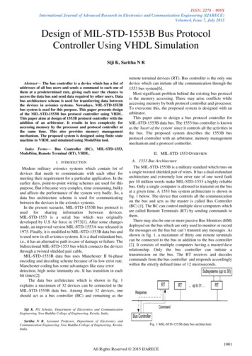
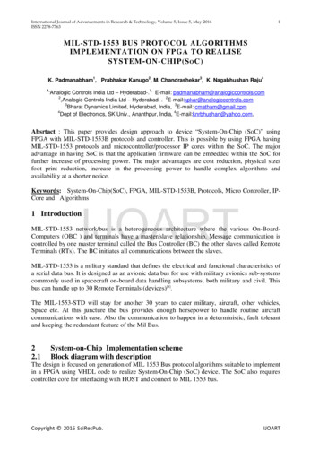
International Journal of Advanced Computer Engineering and Communication Technology (IJACECT)VHDL IMPLEMENTATION OF 1553 PROTOCOL USING ACTELIP CORE1Roopesh N.M, 2Archana & 3Lakshmi Narasimhan1&2CIT, Gubbi, Karnataka, India; 3Scientist/Engineer SD, DSG, ISAC, Bangalore, Karnataka, IndiaEmail: 1roops.nm@gmail.com, 2arc telecom@yahoo.co.in, 3lakshmin@isac.gov.inAbstract- To implement a MIL-STD-1553 compatiblesystem, the options that exist are to use a stand-aloneintegrated circuit or an IP core. Today, with most digitallogic being implemented on FPGAs, the choice of an IPCore is advantageous. One such IP core is Core1553BRMfrom Actel. Core1553BRM provides a complete, MILSTD-1553A and B Bus Controller (BC), Remote Terminal(RT) and Monitor Terminal (MT) and is compatible withlegacy 1553 solutions.II. EXISTING & PROPOSED SYSTEMThe MIL-STD-1553 can be implemented in two ways,they are, stand alone integrated circuit and using IPCore. If it is implemented by using stand aloneintegrated circuit then the overall circuit size in thesatellite is going to increase.Implementations based on stand-alone integrated circuitalong with discrete components increase circuit size. AnIP core implementation shall be useful in reducing theoverall circuit size. So in order to decrease overallcircuit size, a single chip solution i.e. implementationusing IP Core is done.This paper involves study of 1553 architecture and studyof various features of Core1553BRM IP core from Acteland implementation on FPGA. A Bus Controller(BC) andRemote Terminal (RT) are implemented on Actel FPGAand data transfer between the BC and RT isdemonstrated.Since the most digital logic in the satellite is beingimplemented on FPGAs, the 1553 protocol can beimplemented on the same FPGA by using an IP Core onthe same which utilizes the FPGA effectively &decreases the overall circuit size in satellite, hence thechoice of an IP Core is advantageous.Keywords: Bus Controller (BC); Remote Terminal(RT);1553B; Encode; DecodeI. INTRODUCTIONToday the use of digital techniques in spacecraftequipment has greatly increased, as have the number ofsubsystems and the volume of data processed by them.III. 1553B PROTOCOLA. Hardware CharacteristicsBecause analog point-to-point wire bundles areinefficient and cumbersome means of interconnectingthe sensors, computers, actuators, indicators, and otherequipment onboard the spacecraft, a serial digitalmultiplexed data bus was developed. MIL-STD-1553defines all aspects of the bus which is widely used inaircraft systems also.The MIL-STD-1553B bus has four main elements.The 1553 multiplexed data bus provides integrated,centralized system control and a standard interface forall equipment connected to the bus. The bus conceptprovides a means by which all bus traffic is available tobe accessed with a single connection for testing andinterfacing with the system. The standard definesoperation of a serial data bus that interconnects multipledevices via a twisted, shielded pair of wires. The systemimplements a command-response format. A bus controller that manages the informationflow. Remote terminals that interface one or moresimple subsystems to the data bus and respond tocommands from the bus controller. Bus monitor that is used for data bus testing. Data bus components (bus couplers, cabling,terminators and connectors). Data is sequentiallytransmitted and received in a multiplexingscheme over two copper wires from computer tocomputer at a rate of 1 megabit per second.B. Word TypesMIL-STD-1553 gives an effective solution forimplementation of Telemetry and Telecomm and in aspacecraft system. The main onboard computer of aspacecraft can act as a Bus Controller and all othersubsystems can implement a 1553 remote terminal. Thispaper involves the study of 1553B Protocol andimplementation of a BC and RT using IP cores in ActelFPGA.Three distinct word types are defined by the standard.These are: Command words. Data words. Status words.ISSN (Print): 2278-5140, Volume-2, Issue – 2, 20136
International Journal of Advanced Computer Engineering and Communication Technology (IJACECT)Each word type has a unique format, yet all threemaintain a common structure. Each word is twenty bitsin length. The first three bits are used as asynchronization field, thereby allowing the decode lockto re-sync at the beginning of each new word.D. Message FormatThe primary purpose of the data bus is to provide acommon media for the exchange of data betweensystems. The exchange of data is based on messagetransmissions. The standard defines ten types ofmessage transmission formats. All of these formats arebased on the three word types.The next sixteen bits are the information field and aredifferent between the three word types. The last bit isthe parity bit. Parity is based on odd parity for the singleword. The three word types are shown in Fig. 1.The messages transmitted on the data bus includes buscontroller to remote terminal transfers, remote terminalto bus controller transfers, remote terminal to remoteterminal transfers, mode command without data word,mode command with data word (transmit), modecommand with data word (receive), optional broadcastcommand as shown in Figures 2 & 3.A command word shall be comprised of a eceive (T/R) bit, sub address mode field, wordcount/mode code field, and a parity (P) bit. A data wordshall be comprised of a sync waveform, data bits, and aparity bit. A status word shall be comprised of a syncwaveform, RT address, message error bit,instrumentation bit, service request bit, three reservedbits, broadcast command received bit, busy bit,subsystem flag bit, dynamic bus control acceptance bit,terminal flag bit, and a parity bit.Fig 2: Information transfer formatFig 1: Word typesC. EncodingThe data encode shall be Manchester II bi-phase level.A logic one shall be transmitted as a bipolar codedsignal 1/0 (i.e. a positive pulse followed by a negativepulse). A logic zero shall be a bipolar coded signal 0/l(i.e. a negative pulse followed by a positive pulse). Atransition through zero occurs at the midpoint of eachbit time. The transmission bit rate on the bus shall be1.0 megabit per second. The command sync waveformshall be an invalid Manchester waveform. The widthshall be three bit times, with the sync waveform beingpositive for the first one and one-half bit times, and thennegative for the following one and one-half bit times. Ifthe next bit following the sync waveform is a logic zero,then the last half of the sync waveform will have anapparent width of two clock periods due to theManchester encoding.Fig 3: Information transfer format (Broadcast)E. Mode codesMode Codes are defined by the standard to provide thebus controller with data bus management and errorhandling/recovery capability. The mode codes aredivided into two groups: those with, and those without,a data word.The data word that is associated with the mode codes(only one word per mode code is allowed) containsinformation pertinent to the control of the bus and doesnot generally contain information required by thesubsystem (the exception may be the Synchronize withData Word Mode Code). The mode codes are definedby bit times 15-19 of the command word. The mostsignificant bit (bit 15) can be used to differentiatebetween the two-mode code groups.ISSN (Print): 2278-5140, Volume-2, Issue – 2, 20137
International Journal of Advanced Computer Engineering and Communication Technology (IJACECT)The CPU interface allows the system CPU to access thecontrol registers within the core. It also allows the CPUto directly access the memory connected to the backendinterface; this can simplify the system design. The coreincludes thirty-three 16-bit registers. Of the 33 registers,17 are used for control functions and 16 for RTcommand legalization. The RT command legalizationregisters can be omitted from the core, reducing deviceutilization.IV. CORE 1553BRMThe core consists of six main blocks: a 1553 encoder,1553 decoders, a protocol controller block, a CPUinterface, a command word legality interface, and abackend interface as shown in Figure 4.The core can be configured to provide all threefunctions BC, RT, and MT or any combination of thethree. All core variations use all six blocks except forthe command legalization interface, which is onlyrequired in RT functions that implement the RTlegalization function externally.For 1553 receive commands (BC transmits data), thedata pointer determines the location of the data words tobe retrieved. The core will retrieve data wordssequentially from the address specified by the datapointer. Conversely, for a transmit command (BCreceives data), the data pointer determines the memorylocation for data storage.A single 1553 encoder takes each word to betransmitted and serializes it using Manchester encoding.The core stores data words sequentially starting fromthis memory location. After transmission or reception,the core will begin command post processing.Control of the core operating as an RT is accomplishedthrough the use of control words stored in descriptorblocks, and mode codes and sub addresses sent in 1553messages. Control word information allows the core togenerate interrupts, buffer messages, and controlmessage processing. Moreover, the descriptor blockcontains pointers to data buffers where mode codes andsub addresses to be used by the host or subsystem infurther message processing are stored.Figure 4: Core1553BRM Block DiagramThe encoder also includes loopback fail logic andindependent logic to prevent Core1553BRM fromtransmitting for longer than the allowed period. Theloopback logic monitors the received data and verifiesthat the core has correctly received every word that ittransmits. The output of the encoder is gated with thebus enable signals to select which busses the coreshould be transmitting on.For receive commands, the core processes eachincoming message for correct format, word count, andcontiguous data. If a message error is detected, the corewill stop processing the remainder of the message,suppress status word transmission, and set the messageerror bit (ME, bit 9) of the status word.The core will track the message until the end of themessage is detected.Two decoders take the serial Manchester received datafrom each bus and extract the received data words. Thedecoder requires a 12, 16, 20, or 24 MHz clock toextract the data and clock from the serial stream.V. DESIGN AND IMPLEMENTATIONThe BC is designed and implemented as shown inFigure 5.The decoder contains a digital phase-locked loop (PLL)that generates a recovery clock used to sample theincoming serial data. The data is then deserialized andthe 16-bit word decoded. The decoder detects whether acommand, status, or data word has been received andchecks that no Manchester encoding or parity errorshave occurred in the word.The protocol controller block handles all the messagesequencing and error recovery for all three operatingmodes BC, RT, and BM. This is a complex statemachine that processes messages based on the messagetables set up in memory, or reacts to tation varies depending on which functionsare implemented.Figure 5: BC configuration block diagramISSN (Print): 2278-5140, Volume-2, Issue – 2, 20138
International Journal of Advanced Computer Engineering and Communication Technology (IJACECT)To write values to 1553core registers and to monitorcommand blocks we use Core8051, and a 2kX16external memory is used to store command blocks anddata block. Since the same memory is used between8051 and 1553 it is possible that Core1553 andCore8051 read and write in the same location at thesame time. Such conflicts should be avoided by usingarbitration or multiplexer logic.PCI interface isused to write/read TC/TM commands to FPGA TC/TMregisters.data. A user driven thread takes command inputs fromuser for Telecomm and and sends them to PCI registers(TC related) which are then transmitted by BC to RT.Memory FormationSince in BC set up, Core8051 processes 8-bit data andCore 1553 processes 16-bit data, we formed a commonmemory where we can access 8-bit and 16-bit data.Actel’s A3P1000 Proasic3 Evaluation kit supports 4k*9memory block hence we used two 4k*9 memory blocksto form single 2k*16 memory block as shown in Figure7, where one block is used to access lower byte andother block is used to access higher byte data. Thesetwo blocks are differentiated by 8051addr(0) bit onmicrocontroller side.For telecomm and, 8051 programs 1553 for BC byprogramming the CPU interface registers and operationstarts by writing start execution bit. PCI writescommand words into FPGA TC registers.On user request FPGA sends an interrupt to 8051. 8051writes this data to shared memory and Core1553transmits these words on the 1553 bus.For telemetry, a periodic scheduler(counter) is run onthe FPGA once in a second. This interrupts 8051. 8051programs Core1553BC to send TM request to RT.Appropriate locks are put in the BC FPGA to see to itTM and TC requests do not affect each other when theyoccur simultaneously and are scheduled one after theother. On completion, stops BC, writes status to FPGAstatus register.VI. ALGORITHMStep1: StartThe RT is designed and implemented as shown inFigure 6.Step2: Initialize all required signals, 18-bitCounter, Memory, flip flops, Multiplexer etc.Step3: Design 18-bit Counter, required amount ofMemory, flip flop, Multiplexer etc.Step 4: Divide the board clock by 4 to 8051 clock and8051 clock by 32 to 18-bit counter using Flip Flops.Step 5: Using counter generate a pulse for every secondfor TM request.Step 6: Write 8051 code to configure Core1553 BCregisters and to manage TM and TC operation of BC.Step 7: On BC side write VHDL code for arbiter, toprovide signals for INT0 and INT1.Figure 6 : RT Configuration Block DiagramOn RT side we will not use Core 8051 for initializationand controlling instead we used state machine. Core1553 RT receives requests on bus and if the request isTC, it receives all data words and saves in memorylocation allocated for particular sub address/mode code.If the request word is TM, then RT takes TM data savedin memory and sends to BC through the required bus.Step 8: If INT0 occurs 8051 makes 1553 BC to sendtelecomm and by accessing data stored in commonmemory on BC side, on receiving RT saves TC data inits memory and generates appropriate pulses.Step 9: If INT1 occurs 8051 makes 1553 BC to sendtelemetry request to RT then RT sends a data wordsstored in memory on RT side.BC and RT are implemented on Actel A3P1000Proasic3 FPGA. BC is implemented on a PCI card. RTis implemented on an FPGA kit.Step 10: StopVII. RESULTAn application software is designed to handlesimultaneous telemetry and telecomm and requirements,using C on MS Visual Studio.BC and RT designed using Core1553 are interfaced andtested for TM and TC. The results of simulation arerecorded. The BC sends a TC request (command word)and 12 data words, RT receives those 12 TC words andThis software periodically runs a thread to access PCIregisters(TM related) and read and display TelemetryISSN (Print): 2278-5140, Volume-2, Issue – 2, 20139
International Journal of Advanced Computer Engineering and Communication Technology (IJACECT)saves in it memory and generates command pulses onthe RT subsystem, and sends status word back to BC.This is shown in Figure 8-Figure 9.The BC sends a TM request for every 1 sec, uponreceiving this request RT sends status word and requiredamount of data words as shown in Figure 10.Figure 12 : TC & TM in Application SoftwareVIII. CONCLUSIONFigure 8 :BC sending command & data wordsIn this paper the study of 1553 architecture and study ofvarious features of Core1553BRM IP core from Actelare carried out successfully. A Bus Controller(BC) andRemote Terminal (RT) are implemented on an ActelFPGA and data transfer between the BC and RT isdemonstrated successfully.IX. ACKNOWLEDGEMENTOn the completion of my paper, I would like to expressmy deepest gratitude to all those whose kindness andadvice have made this work possible.Figure 9 :RT sending command & data wordsI am greatly indebted to my guides N LakshmiNarasimhan, scientist/engineer SD, DSG, ISAC,Bangalore and Archana sompur, Senior Lecturer, ECEDepartment, CIT, Gubbi who gave me valuablesuggestions. Their effective advice, shrewd commentshave kept the paper in the right direction. I would like tothank my friends for their constructive suggestions.Figure 10 :BC requesting TM & RT replyingX. REFERENCESNext the BC and RT is implemented on FPGA kits, andusing application software TM reception and TCsending is verified as shown in Figure 11-Figure 12.The TC reception on RT is verified by pulses and alsowe made loopback logic for verification and it is shownin Figure 12.Figure 11 : TM in Application Software[1]www.aim-online.com,TUTORIAL, AIM GmbhMIL-STD-1553[2]www.actel.com, Core 1553BRT-EBR EnhancedBit Rate 1553 Remote terminal[3]Ing. Cristian Pérez, Ing. Mauricio Principi, Lic.Ariel Principi, Ing. Diego Fusari, Sr. DiegoBadino, “Bus Monitor Implementation for MILSTD 1553B protocol with FPGA device and PCconnectivity”[4]Interfaces and Standards MIL-STD-1553/1773Basics, NASA Office of Logic Design[5]www.actel.com, Core 1553 BRM[6]www.actel.com, Designing a MIL-STD-1553System Using Core1553 and Core8051[7]Junling Tian, Kai Hu, Huiying Zhang, JianweiNiu, Hong Jiang, “Design of MILSTD-1553BISSN (Print): 2278-5140, Volume-2, Issue – 2, 201310
International Journal of Advanced Computer Engineering and Communication Technology (IJACECT)Protocol Simulation System” 2010 3rdInternational Conference on Advanced ComputerTheory and Engineering. L[8]Iang Zhijian, “Research and Design of 1553BProtocol Bus Control Unit” 2010 InternationalConference on Educational and NetworkTechnology.[9]Myung-Jin Baek, Jong-In Lee, Eun-Sup Sim,Hak-Jung Kim, Joo-Jin Lee, “On-BoardManagement of Multiple Processor SpacecraftSystem” International Conference, 2002 IEEE.[10]www.actel.com, Core 8051 Data Sheet.[11]www.actel.com, Core 1553 Development KitUser Guide ISSN (Print): 2278-5140, Volume-2, Issue – 2, 201311
MIL-STD-1553 defines all aspects of the bus which is widely used in aircraft systems also. The 1553 multiplexed data bus provides integrated, centralized system control and a standard interface for all equipment connected to
