Transcription
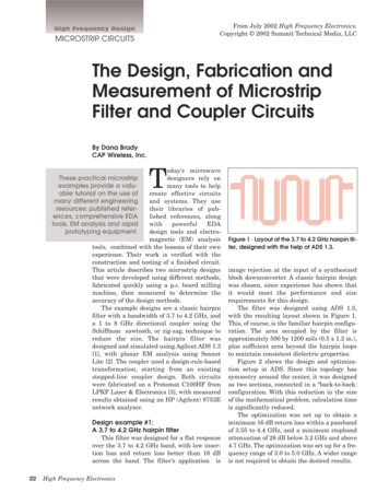
From July 2002 High Frequency Electronics.Copyright 2002 Summit Technical Media, LLCHigh Frequency DesignMICROSTRIP CIRCUITSThe Design, Fabrication andMeasurement of MicrostripFilter and Coupler CircuitsBy Dana BradyCAP Wireless, Inc.Today’s microwavedesigners rely onmany tools to helpcreate effective circuitsand systems. They usetheir libraries of published references, alongwithpowerfulEDAdesign tools and electromagnetic (EM) analysistools, combined with the lessons of their ownexperience. Their work is verified with theconstruction and testing of a finished circuit.This article describes two microstrip designsthat were developed using different methods,fabricated quickly using a p.c. board millingmachine, then measured to determine theaccuracy of the design methods.The example designs are a classic hairpinfilter with a bandwidth of 3.7 to 4.2 GHz, anda 1 to 8 GHz directional coupler using theSchiffman sawtooth, or zig-zag, technique toreduce the size. The hairpin filter wasdesigned and simulated using Agilent ADS 1.3[1], with planar EM analysis using SonnetLite [2]. The coupler used a design-rule-basedtransformation, starting from an existingstepped-line coupler design. Both circuitswere fabricated on a Protomat C100HF fromLPKF Laser & Electronics [3], with measuredresults obtained using an HP (Agilent) 8753Enetwork analyzer.These practical microstripexamples provide a valuable tutorial on the use ofmany different engineeringresources: published references, comprehensive EDAtools, EM analysis and rapidprototyping equipment.Design example #1:A 3.7 to 4.2 GHz hairpin filterThis filter was designed for a flat responseover the 3.7 to 4.2 GHz band, with low insertion loss and return loss better than 16 dBacross the band. The filter’s application is22High Frequency ElectronicsFigure 1 · Layout of the 3.7 to 4.2 GHz hairpin filter, designed with the help of ADS 1.3.image rejection at the input of a synthesizedblock downconverter. A classic hairpin designwas chosen, since experience has shown thatit would meet the performance and sizerequirements for this design.The filter was designed using ADS 1.3,with the resulting layout shown in Figure 1.This, of course, is the familiar hairpin configuration. The area occupied by the filter isapproximately 500 by 1200 mils (0.5 x 1.2 in.),plus sufficient area beyond the hairpin loopsto maintain consistent dielectric properties.Figure 2 shows the design and optimization setup in ADS. Since this topology hassymmetry around the center, it was designedas two sections, connected in a “back-to-back:configuration. With this reduction in the sizeof the mathematical problem, calculation timeis significantly reduced.The optimization was set up to obtain aminimum 16 dB return loss within a passbandof 3.55 to 4.4 GHz, and a minimum stopbandattenuation of 28 dB below 3.2 GHz and above4.7 GHz. The optimization was set up for a frequency range of 3.0 to 5.0 GHz. A wider rangeis not required to obtain the desired results.
High Frequency DesignMICROSTRIP CIRCUITSFigure 2 · Optimization setup in ADS. As noted in the text, the filter was simulated as two “mirror image” sections to exploit the filter’ symmetry.The final ADS design for each“half filter” is shown in Figure 3,including the ports, microstrip lines,tees, bends and stubs. Note the 0.1 pFcapacitances at the end of the stubsto account for end effect (fringingcapacitance). These are also shown inthe layout diagram of Figure 1.Modeled performance is shown inFigure 4. These plots show the passband, stopband, return loss results ofthe ADS simulation, along with aSmith chart plot of input/outputimpedance. These plots show that theADS model meets the filter’s designcriteria.EM analysisFigure 3 · The ADS simulation definition of the final design. Simulated performance data and filter layout are derived from this data.A detailed diagram of the filterdimensions is shown in Figure 5. Thislayout data was used to set up ananalysis of the circuit using the freeSonnet Lite planar electromagneticfield solver software from SonnetSoftware, Inc.Figure 6 shows the results of EManalysis. The passband response isslightly narrower than predicted byADS, but will cover the desired 3.7 to4.2 GHz band if the performance ofthe fabricated circuit matches thisanalysis. Passband flatness is veryclose to that modeled by ADS. Returnloss response is less symmetricalacross the passband than the ADSsimulation, but it remains at 16 dB orbetter.Fabricating a test filterFigure 4 · Simulation results for the filter: (a) overall response, (b) passbandresponse and insertion loss, (c) return loss, and (d) Smith chart impedance24High Frequency ElectronicsTo compare the performance ofthe modeled hairpin filter designwith its real-world counterpart, a testfilter was fabricated on a typicalmicrowave laminate, using a p.c.board milling machine (LPKFProtomat C100HF—see the sidebaron page 29).Layout data from ADS (Figure 1)was used to create the necessarydriver files for the milling machine.These dimensions were transferreddirectly from ADS into the LPKFsetup software. Figure 7 is the layoutfor fabrication of the board.
High Frequency DesignMICROSTRIP CIRCUITSMeasured performanceAfter the board was milled to thedesired pattern, connectors wereattached and the filter was measuredusing an HP 8753E network analyzer. Figure 8 is the through performance (S21) and return loss (S11) ofthe prototype filter. The scale of thisplot is 5 dB per division to show theoverall passband/stopband performance down to –45 dB.Figure 9 is the same as Figure 8,but with the passband plot scaled at1 dB per division to show the passband flatness. The return loss plotremains at 5 dB per division.The measurements show verygood agreement with the models. Thepassband is slightly narrower thanpredicted by ADS, but by a smallerFigure 5 · Detailed dimensions of the hairpin filter.amount than the Sonnet Lite analysis indicated. All three methods ofmodeling and measurement were inagreement on the insertion loss andthe flatness of the passband.Although there are variations inFigure 6 · EM analysis results from Sonnet Lite, which indicates that the response satisfies the design criteria.Figure 7 · Circuit board layout for milling with the LPKFmachine.Figure 8 · Passband and return loss measurement of theprototype filter on a milled p.c. board.Figure 9 · Same as Figure 8, but 1 dB per division resolutionto obtain a detailed passband measurement.26High Frequency Electronics
High Frequency DesignMICROSTRIP CIRCUITSFigure 10 · This basic layout (left) and fabrication template (right) illustrate the technique used for the Schiffmanreduced-size directional coupler.the shape of the return loss plotsamong the modeled and measureddata, each of them maintains thedesired 16 dB specification, andclearly shows the expected “humps”of a multi-pole filter response.The next circuit we’ll examinewas developed using an empiricaltechnique. We wanted to investigatea method of reducing the size ofmicrostrip circuits developed bySchiffman, as described by Uysal [4].This technique uses a sawtooth orzig-zag pattern to reduce themechanical length required for agiven electrical length.An existing 1 to 8 GHz steppedline coupler, designed in ADS by CAPWireless colleague Paul Daughenbaugh, was used as the startingpoint. This design was translated intoa layout for fabrication on the millingmachine, similar to the one shown inFigure 10. This figure actually showsa different version of the coupler, butit clearly illustrates the technique.An empirical method was used toobtain the new coupler layout fromthe straight-section coupler design,using the following rules: Close-spaced coupler section—The total length along the zig-zagpath was made equal to the straightline length of this section. Thisreduced the length of this section bya factor of nearly half. The spacingbetween straight lines was maintained between the “interlocking”teeth, as measured across the gaps atright angles to their edges. Wide-spaced coupler section—The spacing between the lines of thethird section was calculated at themid-height of the teeth. At this widespacing, it was assumed that thefields would couple according to thisaverage spacing, rather than alongthe edge path of the first section.Also, the length reduction is less inthis section. For simplicity, the samelength as the original straight linesection was used. Center section—The line spacingand the length reduction of the centersection was calculated as the geometric mean of the first and third sections.This “best guess” approach wasnecessary because it was not possibleto analyze this structure using theavailable software tools. It is too complicated for analysis with SonnetFigure 11 · Coupled port transmissionand input port return loss.Figure 12 · Reverse coupling and output port return loss.Figure 13 · Insertion loss (verticalscale is 0.5 dB per division).Design example #2:A reduced-size stepped-linedirectional coupler28High Frequency Electronics
Lite, and other analysis tools werenot available.Coupler performanceAfter fabrication with the LPKFmilling machine, the coupler wasevaluated for the degree of coupling,directivity across the 1 to 8 GHzband. In Figure 11, the coupled porttransmission is the smooth line. Thehorizontal line at the center of plot is–18 dB and the grid is 2 dB per division. Coupling is –19 dB 1.5 dB overthe measured frequency range. In thesame figure, input return loss is plotted at 5 dB per division, referenced to0 dB at the second line from the top.Worst case return loss is 16 dB at thelowest frequencies.Reverse coupling is plotted inFigure 12, along with output portreturn loss. Both plots are 5 dB perdivision. For reverse coupling, thecenter line is the reference, again at–18 dB, and coupling is –28 dB or better across the band, better than 31 dBat all but the high frequency end. Theoutput port return loss is plottedusing the same scale as input returnloss in Figure 11, and also shows thesame 16 dB worst case performanceat 1 GHz.Directivity (forward couplingUsing a Milling Machine for p.c. Board PrototypingThe positioning accuracy of themachine is very important, to maintain the necessary precision for bothx-y axis dimensions and the depth ofpenetration. The machine must reliably cut the entire copper claddinglayer, while removing a minimalamount of the underlying dielectricmaterial.50 micron and 10 micron scale references at the bottom of the photos.The milling equipment used atCAP Wireless is the modelProtomat C100HF from LPKFLaser & Electronics. This unit canaccommodate a board up to 13.5 x 8inches (340 x 200 mm). In additionto circuit boards, the unit can millaluminum or brass mechanicalparts or cut copper shielding foils.The motor operates at variablespeeds from 10,000 to 100,000 RPM,software controlled. The typicalfine-pitch milling tool for boardslike those described in this article isa 10 mil endmill, specified for adiameter variation of 0.2 mils:The photo above is a closeup ofthe milling head. The C100HF usesdynamic z-axis positioning with acoaxial working depth limiter tomaintain the milling depth. Thepenetration into the substrate istypically 0.2 mil (5 micron). The zaxis movement range is 14 mm(0.55 in.). An air bearing providesaccurate, but non-contact surfacesensing on soft or flexible boards,and on surface-sensitive materials.The x-y positioning accuracy isless than 0.2 mil (5 micron) at a resolution of 0.3125 mil (7.9 micron).The following electron microscopephotos show a milled path at twodifferent magnifications—note theWith a travel speed of 40 mm/sec(1.575 in.), both fine-pitch millingand runout of large areas is accomplished efficiently. If necessary, it ispossible to build and test severaliterations of a board design in a day.In some cases, the unit will be anacceptable alternative to conventional etched p.c. board fabricationfor custom designs and small-quantity production.Readers wishing to find out moreabout this unit may contact LPKFLaser & Electronics by telephone at1-800-345-LPKF (1-800-345-5653),by e-mail at info@lpkfusa.com, oronline at www.lpkfusa.comJuly 200229
High Frequency DesignMICROSTRIP CIRCUITSFigure 14 · Photo of the 3.7 to 4.2 GHz hairpin filter prototype board.minus reverse coupling) is 10 dB overall but the extreme high end of theband. The design goal was 10 dB,with a target of 12 dB to allow extramargin. This margin was achievedover most of the band, which we consider to be an excellent result for afirst iteration.Figure 13 is insertion loss, whichis 0.25 dB at 1 GHz, with a worst caseof 0.57 dB at 6 GHz. The variation ininsertion loss is just 0.33 dB acrossthe entire 1 to 8 GHz band.Figure 15 · Photo of the 1 to 8 GHz broadband couplerusing the Schiffman, or zig-zag line, technique.The coupler design may yet bemodified to improve low-end returnloss or flatten the coupling response.These small changes would probablynot be considered with conventionalfabrication using an outside boardshop. Most companies no longermaintain in-house board etchinglabs, since environmental regulations, particularly in California, addsignificant cost and complexity to thechemical etching process.SummaryNotes on prototyping with a p.c.board milling machineThe ability to quickly fabricate aprototype p.c. board can change theengineering approach to certaindesigns. For the directional coupler,we were prepared for the possibilitythat several design iterations wouldbe required to obtain a coupler withthe desired performance. With someluck (and educated guesses based onexperience), the first attempt resulted in a good coupler.The photos in Figures 14 and 15show the milled boards, with connectors attached for measurement. Thehairpin filter board in Figure 14 evenshows a patch soldered in place tocover a gap in one of the microstriptraces. This was caused by a smallerror in the layout file that becameevident when the board was milled.30High Frequency ElectronicsIt is hoped that these designexamples show how we used manydifferent design resources. To createthese filter and coupler circuits, theexperience of several engineers wascombined with published data,advanced circuit theory simulation,EM analysis and, finally, fabricationand measurement. Each step in theprocess contributed to the overalldesign success.References1. Agilent Technologies, Inc.; information at www.agilent.com2. Sonnet Software; information at:www.sonnetusa.com3. LPKF Laser & Electronics; information at: www.lpkfusa.com4. Sener Uysal, Nonuniform LineMicrostrip Directional Couplers andFilters, Artech House, 1993.Additional Design References5. G. Matthei, L. Young, E.M.T. Jones,MicrowaveFilters,ImpedanceMatching Networks, and CouplingStructures, Artech House, ISBN 089006-099-1.6. J.A.G. Mahlerbe, MicrowaveTransmission Line Filters, ArtechHouse, ISBN 0-89006-063-0.About the AuthorDana Brady is Senior Engineer atCAP Wireless, Camarillo, CA.Previously, he has held SeniorEngineer positions at CaliforniaAmplifier, Armatek and Amplica, andthe Chief Scientist position at JCATechnology. He attended CaliforniaPolytechnic State University and hasexperience in the design of many RFand microwave circuits and systems,including various microprocessorcontrolled microwave subsystems. Hecan be reached by e-mail at: danab@capwireless.comTo submit a technical article for our consideration, simply e-mail a briefdescription to: editor@highfrequencyelectronics.com Author guidelinescan be found on our web site: www.highfrequencyelectronics.com
results obtained using an HP (Agilent) 8753E network analyzer. Design example #1: A 3.7 to 4.2 GHz hairpin filter This filter was designed for a flat response over the 3.7 to 4.2 GHz band, with low inser-tion loss and return loss better than 16 dB across the band. The filter’s app