Transcription
A Load Balancing Technique for Memory ChannelsByoungchan OhNam Sung KimJeongseob AhnUniversity of MichiganAnn Arbor, Michiganbcoh@umich.eduUniversity of Illinois atUrbana-ChampaignChampaign, Illinoisnskim@illinois.eduAjou UniversitySuwon, Koreajsahn@ajou.ac.krBingchao LiRonald G. DreslinskiTrevor MudgeCivil Aviation University of ChinaTianjin, Chinabcli@cauc.edu.cnUniversity of MichiganAnn Arbor, Michiganrdreslin@umich.eduUniversity of MichiganAnn Arbor, Michigantnm@umich.eduABSTRACTThe performance needs of memory systems caused by growingvolumes of data from emerging applications, such as machinelearning and big data analytics, have continued to increase.As a result, HBM has been introduced in GPUs and throughput oriented processors. HBM is a stack of multiple DRAMdevices across a number of memory channels. Although HBMprovides a large number of channels and high peak bandwidth, we observed that all channels are not evenly utilizedand often only one or few channels are highly congested afterapplying the hashing technique to randomize the translatedphysical memory address.To solve this issue, we propose a cost-effective technique toimprove load balancing for HBM channels. In the proposedmemory system, a memory request from a busy channel canbe migrated to other non-busy channels and serviced in theother channels. Moreover, this request migration reducesstalls by memory controllers, because the depth of a memoryrequest queue in a memory controller is effectively increasedby the migration. The improved load balancing of memorychannels shows a 10.1% increase in performance for GPGPUworkloads.CCS CONCEPTS Hardware Dynamic memory; Computer systems organization Single instruction, multiple data;KEYWORDSDRAM, HBM, GPU, Memory Controller, Work StealingACM Reference Format:Byoungchan Oh, Nam Sung Kim, Jeongseob Ahn, Bingchao Li,Ronald G. Dreslinski, and Trevor Mudge. 2018. A Load BalancingPermission to make digital or hard copies of all or part of this workfor personal or classroom use is granted without fee provided thatcopies are not made or distributed for profit or commercial advantageand that copies bear this notice and the full citation on the firstpage. Copyrights for components of this work owned by others thanACM must be honored. Abstracting with credit is permitted. To copyotherwise, or republish, to post on servers or to redistribute to lists,requires prior specific permission and/or a fee. Request permissionsfrom permissions@acm.org.MEMSYS, October 1–4, 2018, Old Town Alexandria, VA, USA 2018 Association for Computing Machinery.ACM ISBN 978-1-4503-6475-1/18/10. . . que for Memory Channels. In The International Symposiumon Memory Systems (MEMSYS), October 1–4, 2018, Old TownAlexandria, VA, USA. ACM, New York, NY, USA, 12 ODUCTIONGraphic Processing Units (GPUs) have developed for 3Dgraphics, games, and animations, and evolved for generalpurpose high performance computing [13, 21, 27]. GPU’son-chip computing capability has been improved rapidly inthe past two decades [10]. However, the scaling of off-chipmemory bandwidth has not followed the increasing computing capability. Thus, the memory bandwidth often becomesa bottleneck limiting application performance [19]. Traditionally, GDDR memories have been used for GPUs. They arethroughput-optimized DDR and whose the latest generationis GDDR5. However, GDDR5 has challenges in increasingmemory bandwidth, because its interface is narrow (16 or32 per chip) and fast (up to 7Gbps per pin). Although highdate rate is good for high bandwidth, it can only be achievedby consuming high power. In addition, the small number ofI/Os provided from GDDR5 requires many memory chips tobe accommodated in GPUs to achieve high bandwidth. As aresult, the required power and area make GDDR5 prohibitivebeyond 1 TB/s of memory bandwidth [8].High Bandwidth Memory (HBM) has been developed toovercome limited bandwidth of GDDR5 under the givenpower budget and form factor [1, 17, 26]. HBM is an onpackage stacked DRAM and provides high peak bandwidth( 256 GB/s) through multiple (up to 8) and wide channels(128 I/Os per channel). For the power efficiency, data rate(i.e., double of clock speed in DDR) and thus supply voltage are lowered in HBM, but the increased number of I/Osand channels results in higher peak bandwidth than that ofGDDR5-based GPUs. In other words, the high peak bandwidth of HBM stems from a number of memory channels.Therefore, high bandwidth can be achieved in HBM when allHBM channels are utilized well. However, it is hard to evenlyutilize all memory channels for all applications because eachapplication has different memory access pattern. Moreover,substantial imbalance on memory channels still remains after
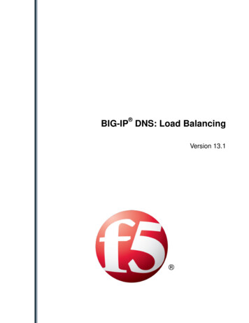
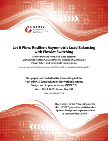
MEMSYS, October 1–4, 2018, Old Town Alexandria, VA, USA2 BACKGROUND2.1 Increasing Demand of Memory Capacity andBandwidthThe increasing volume of data to be processed by machinelearning and big data analytics demands data parallel architectures such as Single Instruction Multiple Data (SIMD)Off ChipDRAMStackedDRAMM.CM. CM.CtHos orscesProM.CtHos orscesProM.Capplying an XOR-based address mapping scheme, which randomizes the address mapping to avoid excessive contentionon one or few memory channels/banks [35, 36].To address this issue, we propose a cost-effective techniqueto improve load balancing for HBM channels. Our techniqueis conceptually similar with the work stealing technique usedin multi-core scheduling, where an idle core steals a workitem in a busy core and the load is balanced across multiplecores [4, 25]. Similarly, in our proposed HBM-based memorysub-system, a memory request in a busy channel is migratedto another non-busy channel and issued through that channel.Then, the migrated request is rerouted to its original memory device. However, in traditional GDDR5-based memorysub-systems, this simple load balancing technique is hardto apply because of mainly two reasons. First, memory controllers and their physical channels are placed on the differentside of the host processor chip. Thus, the memory requestmigration requires global interconnection across the wholechip. Second, in order to reroute the migrated requests, extraoff-chip interconnections to connect all off-chip GDDR5 chipsare needed. Considering the cost to implement extra internaland external interconnections, the load balancing on memorychannels by migration and rerouting would be impractical inthe traditional GDDR5-based system. However, unlike theGDDR5-based system, the HBM-based system has severaladvantages in implementing this load balancing technique.First, multiple memory controllers for one HBM are locallyplaced because they are connected to the same chip havingmultiple DRAM devices. Thus, the local interconnections canenable the memory request migration. Second, one HBM has8 channel. The DRAM dies have multiple ports that combineto form the 8 channels. Rerouting of the memory request canbe performed inside of HBM. Because each DRAM die for achannel has the physical connection of all TSVs and this connection can be electrically controlled, a simple modificationin HBM can implement the rerouting.In our proposed memory system, if a channel is highly congested whereas other channels are not, the memory requestmigration is triggered. Then, the migrated memory requestis rerouted to its original DRAM device by controlling electrical connection of TSVs in HBM. Through this balancingtechnique, the imbalance on memory channels is reduced by7% on average. Moreover, because this request migrationeffectively increases the depth of memory request queue in amemory controller by occupying other memory controller’squeue, the stall by memory sub-system is reduced. Theseimproved load balancing and queue depth, in turn, bring10.1% of GPU performance improvement (up to 26%).Byoungchan Oh et al.M.CM.CM.C: MemoryControllerGDDR5-based GPU SystemInterposerHBM-based GPU SystemFigure 1: GPU systems with GDDR5 and HBM.DRAM BISTMUXCH0ENDQENeFuseDecoderENIEEE15008-CH 2CH0Logic DieCH7CH5CH3CH1CH7CH5CH3CH1Logic DieFigure 2: 3D structure of an HBM and a simple example ofTSV connections to DRAM dies.and Single Instruction Multiple Threads (SIMT) architectures [12, 32]. Especially, GPUs become the de facto standardand, in turn, the state-of-the-art servers in clouds and datacenters are equipped with GPUs to speed up general purposecomputation (i.e., General Purpose computing on GraphicsProcessing Units (GPGPU)) [27]. Because GPUs have beendesigned to improve the throughput of applications by spawning many threads simultaneously, the capacity and bandwidthof memory have played an essential role in building high performance applications. For example, in many programmingmodels in GPGPU applications such as nearest neighborclassifiers, decision trees, and neural networks, the size ofGPU memory often imposes limitations on the data size, resulting in decreased performance by continually transferringdata from the system’s memory to the GPU’s memory [6]. Inaddition, because many of GPGPU applications are memoryintensive and sometimes exhibit irregularity in their memoryaccess patterns, their performance is significantly affected bymemory bandwidth [5].2.2High Bandwidth MemoryHBM and HBM-based systems. Memory bandwidth has beencontinuously increased to meet GPU performance growth.However, in traditional GDDR5-based systems, there aremainly two challenges in increasing memory bandwidth. First,
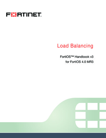
In this study, we take HBM generation 2 (HBM2) as a baseline.However, we do not differentiate HBM and HBM2 in this study becausemain features of them, such as wide I/O, multi channels and 3D stackedDRAM dies, are almost same.1BANK 0BANK 2BANK 4BANK 6Shared I/OBANK 1BANK 3BANK 5MEM CHBANK 7BANK 0BANK 3Shared I/O(a) Memory organization without bank groupBANK GROUP 0BANK 2BANK 4MEM CHMULTIPLEXBANK 0BANK 3Shared I/Othe increased memory bandwidth brings a significant increasein the power budget for memory and this power budgetis becoming prohibitive as the bandwidth scales beyond 1TB/s [8]. Because GDRR5 is connected to a host processorthrough fast (up to 7Gbps per pin) and narrow (16 or 32per chip) external I/O interface, its energy-per-bit presentshigh ( 14pJ/bit). Second, GDDR5 can limit form factors.As shown in Fig. 1(left), GDDR5 requires a large number ofmemory chips to reach high bandwidth because of its narrowchannel. Also, to build a large memory system with a givendensity of GDDR5, more memory chips are needed. Thelarge footprint by GDDR5 does not only affect form factors,but this also degrades the signal integrity on the memoryinterface because of long connection distance [15, 23].HBM, which is an on-package stacked DRAM, has beenintroduced to overcome power and form factor challengesof GDDR5. Unlike GDDR5, HBM employs a slow ( 2Gbpsper pin) and wide (128 per channel) channel and accordinglysupply voltage becomes lowered (1.5V - 1.2V)1 . In addition,since HBM has multiple stacked DRAM dies and is connectedto the host processor via silicon interposer within a package,this system can accommodate a large number of memorydevices with a small space as shown in Fig. 1(right).TSV connections. Fig. 2 depicts the internal structure ofHBM. An HBM is made with various capacity, the number ofstacked layers and channel configurations [17]. In this study,the baseline HBM has 1Gb capacity and 2 half-channels perDRAM die and total 8 DRAM dies (total 8Gb). All DRAMdies are fabricated identically and thus all they are physicallyconnected to TSVs for 8 channels. Then, a set of TSVs forcertain channels can be electrically connected to one of theDRAM dies by using tri-state buffers with the decoder logicshown in the left of Fig. 2. During a manufacturing step, aStack ID (SID) is programmed to the decoder to enable ordisable the tri-state buffers by using electrical fuses (efuses).We describe an example of this physical and electrical connections between TSVs and DRAM dies in Fig. 2(right), wherethe set of TSVs have physical connections to both DRAMdies but only the bottom DRAM die for CH0 is electricallyconnected to the TSVs.Bank group structure. The bank group feature, which is usedin GDDR5 and DDR4, is, also, adopted in HBM [17, 18, 24].We describe the organization of a DRAM device with andwithout the bank group feature in Fig. 3. As shown in Fig. 3a,all banks are connected to one internal shared data bus. Traditionally, in order to bridge the gap between slow datatransfer speed on the shared bus and fast interface speed,data are transferred on the shared bus in parallel and thenserialized out the interface with multiple clock cycles (a.k.an-prefetch). In this structure, if the speed gap is increased,the prefetch length and accordingly burst length, which determine memory transaction and LLC line sizes, should beMEMSYS, October 1–4, 2018, Old Town Alexandria, VA, USABANK GROUP 1A Load Balancing Technique for Memory ChannelsBANK 2BANK 4(b) Memory organization with bank groupFigure 3: Comparison between two memory organizations [24].increased together to keep seamless burst read/write operations. Furthermore, bank-level parallelism in this structuredoes not improve much with the number of banks because ofthe limited scalability of the single shared bus. In order toavoid increasing prefetch length and improve the parallelism,the bank group feature has been introduced as depicted inFig. 3b. In the bank group structure, multiple banks groups(typically, 4 or 8 groups, 4 by default in this study) have theirown internal data bus and multiple banks (2 or 4 banks, 4 bydefault) in a bank group share one data bus. As the resultof the separated data bus, multiple sets of data can be concurrently transferred between the interface and bank groups.However, different timing constraints, tCCDS and tCCDL, areapplied when accessing banks in different bank groups andthe same bank group, respectively. tCCDL is the minimumtime between two read commands (or write commands) whenaccessing the same bank group and determined by the datatransfer time on the shared data bus in the bank group.However, tCCDS is the minimum time between two read commands (or write commands) when accessing different bankgroups and not determined by the data transfer time becausetwo read accesses are served on different buses in different
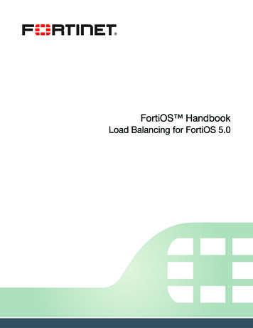
MEMSYS, October 1–4, 2018, Old Town Alexandria, VA, USA1.5Skewness1.42.514Byoungchan Oh et al.# of Memory RequestMemory Service Time1.31.2Steal1.11.0Scheduler 0Scheduler 1Processor 0Processor 10.9Figure 4: Channel utilization and memory service time.Figure 5: Simple diagram for work stealing.bank groups. Thus, the bank level parallelism in a bank groupis still preserved, but the bank group level parallelism is ahigher degree of parallelism.3CHALLENGES IN MANY CHANNELMEMORY SYSTEMS3.1 Imbalanced Channel UtilizationIn general, the memory address mapping scheme is designedconsidering both spatial locality and parallelism [7]. For example, consecutive cache line accesses are scheduled to thesame row in the same bank to take advantage of shorterlatency when row buffer hit. On the other hand, accessingblocks of cache line alternates between multiple banks andchannels by exploiting bank- and channel-level parallelism.However, depending on workloads memory system can suffer from excessive contention on one or few certain banksand channels. To prevent this situation, a permutation-basedmapping scheme (i.e., hashing), in which channel and bankselections are determined by XORing a subset of MSB-sidebits, has been proposed [35, 36]. Although this technique partially randomizes memory accesses, it is hard to completelyeliminate the imbalanced memory requests on all channelsand banks.Fig. 4 shows the skewness of total memory requests andservice time across 8 channels of an HBM. The skewness isdefined to the ratio of the minimum value to the maximumvalue. If the address mapping scheme is ideal and thus allchannels receive the equal number of memory requests, theskewness of total memory requests becomes 1. Although theskewness of total memory requests is closed to 1 in manyworkloads due to XORing applied in the address mappingscheme, some workloads exhibit high skewness. Furthermore,this imbalance on the total number of memory requestsis amplified on the service time, which is defined to thetotal time spent to serve all memory requests in a memorycontroller, as shown in Fig. 4. Because spatial and temporallocality in each channel can be different with the same numberof requests, they can make different scheduling scenario andresult in non-equal memory service time in each channel.The imbalanced memory requests and utilization across thememory channels can negatively affect overall performanceby hindering exploiting full capability of all memory channels.Work stealing, which is a well-known scheduling technique formulti-core systems, has been proposed to balance workloadsand improve performance [4, 25]. We describe the simplifiedmechanism of the work stealing in Fig. 5. If a processor is idle(processor 1) is idle, it looks at the queue of another processor(processor 0) and steals its work if there are outstandingworks. In this case, because all processors are identical, awork item can be executed in any processor. Therefore, theload balancing technique for memory channels like the workstealing can be considered to a good solution for imbalancedmemory channels. However, the load balancing techniquecannot be simply applied to the traditional GDDR5-basedsystem, because each memory request (the work item in thework stealing) has its own memory address and it must beserved in the preassigned memory device by the address.In other words, if a memory request is migrated to otherchannels and issued through the other channels, it must bererouted and served in its initially assigned memory devicebased on the address.3.2Implementation Challenges of MemoryControllersHaving large request queues in the memory controller is generally beneficial to the performance because of mainly tworeasons. First, the request queue is the buffer to mitigate thegap between fast input and slow service speeds of memoryrequests [22]. Thus, the queue depth determines the capability to hold the number of outstanding requests and thiscan significantly affect the performance when workloads arememory-intensive. Second, there are more chances to makebetter scheduling decisions (i.e., shorter latency) in largerqueues [2]. For instance, a First-Ready First-Come-FirstServed (FR-FCFS [29, 38]) scheduler can make more rowhits with a larger queue because the scheduler observes morememory requests and this increases the probability to find
A Load Balancing Technique for Memory ChannelsMEMSYS, October 1–4, 2018, Old Town Alexandria, VA, USA1.4Full !2nd LevelQueue1.11.00.9SchedulerSchedulerNormalized IPC1.21st 81.3CH0CH1Original queueFigure 6: Performance according to the queue depth.CH0CH1Unified hierarchical queueFigure 8: Hierarchical queue structure.CH NCommand QueueOrdering LogicBank NBank 0Open Row AddComparator Hit CmdTransactionProcessingWrite QueueRead Queueindependent memory controller. Therefore, the area of memory controllers has a significant impact on total chip area inmany channel memory systems.CH2CH1CH0ArbiterCMD(CH N)DATA(CH N)CMD(CH0)DATA(CH0)Timing RegistersFigure 7: Schedulers of the memory controller in many channel memory systems [16].memory requests corresponding to the scheduling priority.However, there are fewer row hits with a smaller queue because of limited visibility to memory requests. Fig. 6 depictsthe performance improvement according to the number ofqueue entries with various GPGPU applications. Based onworkloads and their memory intensity, the
A Load Balancing Technique for Memory Channels Byoungchan Oh University of Michigan Ann Arbor, Michigan bcoh@umich.edu Nam Sung Kim University of Illinois at Urbana-Champaign Champaign, Illinois nskim@illinois.edu Jeongseob Ahn Ajou University Suwon, Korea jsahn@ajou.ac.kr Bingchao Li Civil