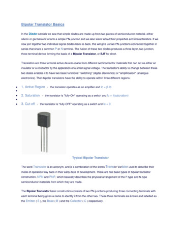
Transcription
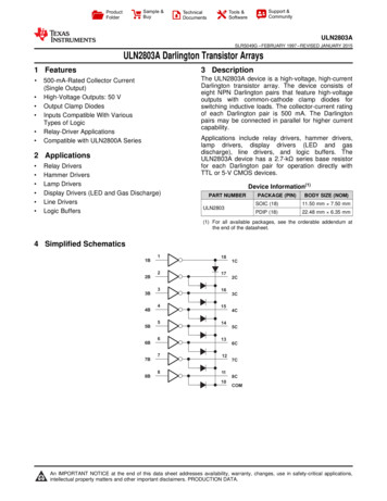
Sample &BuyProductFolderSupport &CommunityTools &SoftwareTechnicalDocumentsULN2803ASLRS049G – FEBRUARY 1997 – REVISED JANUARY 2015ULN2803A Darlington Transistor Arrays1 Features3 Description The ULN2803A device is a high-voltage, high-currentDarlington transistor array. The device consists ofeight NPN Darlington pairs that feature high-voltageoutputs with common-cathode clamp diodes forswitching inductive loads. The collector-current ratingof each Darlington pair is 500 mA. The Darlingtonpairs may be connected in parallel for higher currentcapability.1 500-mA-Rated Collector Current(Single Output)High-Voltage Outputs: 50 VOutput Clamp DiodesInputs Compatible With VariousTypes of LogicRelay-Driver ApplicationsCompatible with ULN2800A Series2 Applications Relay DriversHammer DriversLamp DriversDisplay Drivers (LED and Gas Discharge)Line DriversLogic BuffersApplications include relay drivers, hammer drivers,lamp drivers, display drivers (LED and gasdischarge), line drivers, and logic buffers. TheULN2803A device has a 2.7-kΩ series base resistorfor each Darlington pair for operation directly withTTL or 5-V CMOS devices.Device Information(1)PART NUMBERULN2803PACKAGE (PIN)BODY SIZE (NOM)SOIC (18)11.50 mm 7.50 mmPDIP (18)22.48 mm 6.35 mm(1) For all available packages, see the orderable addendum atthe end of the datasheet.4 Simplified 6C7127B7C8118B8C10COM1An IMPORTANT NOTICE at the end of this data sheet addresses availability, warranty, changes, use in safety-critical applications,intellectual property matters and other important disclaimers. PRODUCTION DATA.
ULN2803ASLRS049G – FEBRUARY 1997 – REVISED JANUARY 2015www.ti.comTable of Contents123456789Features .Applications .Description .Simplified Schematics.Revision History.Pin Configuration and Functions 5Absolute Maximum Ratings .ESD Ratings.Recommended Operating Conditions.Thermal Information .Electrical Characteristics.Switching Characteristics .Typical Characteristics .Parameter Measurement Information . 7Detailed Description . 109.19.29.39.4Overview .Functional Block Diagram .Feature Description.Device Functional Modes.1010101010 Application and Implementation. 1110.1 Application Information. 1110.2 Typical Application . 1111 Power Supply Recommendations . 1312 Layout. 1312.1 Layout Guidelines . 1312.2 Layout Example . 1313 Device and Documentation Support . 1413.1 Trademarks . 1413.2 Electrostatic Discharge Caution . 1413.3 Glossary . 1414 Mechanical, Packaging, and OrderableInformation . 145 Revision HistoryChanges from Revision F (January 2014) to Revision G PageAdded Applications, Device Information table, Pin Functions table, ESD Ratings table, Thermal Information table,Typical Characteristics, Feature Description section, Device Functional Modes, Application and Implementationsection, Power Supply Recommendations section, Layout section, Device and Documentation Support section, andMechanical, Packaging, and Orderable Information section. . 1Changes from Revision E (July 2006) to Revision FPage Updated document to new TI data sheet format - no specification changes. . 1 Deleted Ordering Information table. . 12Submit Documentation FeedbackCopyright 1997–2015, Texas Instruments IncorporatedProduct Folder Links: ULN2803A
ULN2803Awww.ti.comSLRS049G – FEBRUARY 1997 – REVISED JANUARY 20156 Pin Configuration and FunctionsDW OR N PACKAGE(TOP 01C2C3C4C5C6C7C8CCOMPin FunctionsPINNAMENO.TYPEDESCRIPTION 1:8 B1-8IChannel 1 through 7 darlington base input 1:8 C18 - 11OChannel 1 through 7 darlington collector outputGND7—Common Emmitter shared by all channels (typically tied to ground)COM8I/OCommon cathode node for flyback diodes (required for inductive loads)Submit Documentation FeedbackCopyright 1997–2015, Texas Instruments IncorporatedProduct Folder Links: ULN2803A3
ULN2803ASLRS049G – FEBRUARY 1997 – REVISED JANUARY 2015www.ti.com7 Specifications7.1 Absolute Maximum Ratingsat 25 C free-air temperature (unless otherwise noted) (1)MINMAXCollector-emitter voltageInput voltage(2)(1)(2)V30VPeak collector current500mAOutput clamp current500mATotal substrate-terminal currentTJUNIT50Operating virtual junction temperature–65–2.5A150 CStresses beyond those listed under Absolute Maximum Ratings may cause permanent damage to the device. These are stress ratingsonly, and functional operation of the device at these or any other conditions beyond those indicated under Recommended OperatingConditions is not implied. Exposure to absolute-maximum-rated conditions for extended periods may affect device reliability.All voltage values, unless otherwise noted, are with respect to the emitter/substrate terminal GND.7.2 ESD RatingsVALUEV(ESD)(1)(2)Electrostatic dischargeHuman body model (HBM), per ANSI/ESDA/JEDEC JS-001, all pins (1) 2000Charged device model (CDM), per JEDEC specification JESD22-C101,all pins (2) 500UNITVJEDEC document JEP155 states that 500-V HBM allows safe manufacturing with a standard ESD control process.JEDEC document JEP157 states that 250-V CDM allows safe manufacturing with a standard ESD control process.7.3 Recommended Operating Conditionsover operating free-air temperature range (unless otherwise noted)MINMAXVI05VVCC050V-40125 CTJJunction TemperatureUNIT7.4 Thermal InformationULN2803ATHERMAL METRIC (1)DDW18 PINS18 PINSRθJAJunction-to-ambient thermal resistance7366.4RθJC(top)Junction-to-case (top) thermal resistance40.329.5RθJBJunction-to-board thermal resistance38.933.0ψJTJunction-to-top characterization parameter10.96.0ψJBJunction-to-board characterization parameter38.732.5RθJC(bot)Junction-to-case (bottom) thermal resistanceN/AN/A(1)4UNIT C/WFor more information about traditional and new thermal metrics, see the IC Package Thermal Metrics application report, SPRA953.Submit Documentation FeedbackCopyright 1997–2015, Texas Instruments IncorporatedProduct Folder Links: ULN2803A
ULN2803Awww.ti.comSLRS049G – FEBRUARY 1997 – REVISED JANUARY 20157.5 Electrical Characteristicsat TA 25 C free-air temperature (unless otherwise noted)PARAMETERULN2803ATEST CONDITIONSMINICEXCollector cutoff currentVCE 50 V,see Figure 4II 0II(off)Off-state input currentVCE 50 V,TA 70 CIC 500 μA,see Figure 5II(on)Input currentVI 3.85 V,See Figure 6VI(on)VCE 2 V,see Figure 7On-state input voltageVCE(sat)Collector-emitter saturation voltageTYPMAX5050μAμA650.93UNIT1.35IC 200 mA2.4IC 250 mA2.7IC 300 mA3II 250 μA,see Figure 8IC 100 mA0.91.1II 350 μA,see Figure 8IC 200 mA11.3II 500 μA,see Figure 8IC 350 mA1.31.650mAVVμAIRClamp diode reverse currentVR 50 V,see Figure 9VFClamp diode forward voltageIF 350 mAsee Figure 101.72VCiInput capacitanceVI 0,f 1 MHz1525pFTYPMAX7.6 Switching CharacteristicsTA 25 CPARAMETERTEST CONDITIONSMINtPLHPropagation delay time, low- to high-level output130tPHLPropagation delay time, high- to low-level outputVS 50 V, CL 15 pF, RL 163 Ω,See Figure 11VOHHigh-level output voltage after switchingVS 50 V, IO 300 mA, See Figure 1220VS – 20UNITnsmV7.7 Typical CharacteristicsFigure 1. Collector-Emitter Saturation VoltagevsCollector Current (One Darlington)Figure 2. Collector-Emitter Saturation VoltagevsTotal Collector Current (Two Darlingtons in Parallel)Submit Documentation FeedbackCopyright 1997–2015, Texas Instruments IncorporatedProduct Folder Links: ULN2803A5
ULN2803ASLRS049G – FEBRUARY 1997 – REVISED JANUARY 2015www.ti.comTypical Characteristics (continued)Figure 3. Output Current vs Input Current6Submit Documentation FeedbackCopyright 1997–2015, Texas Instruments IncorporatedProduct Folder Links: ULN2803A
ULN2803Awww.ti.comSLRS049G – FEBRUARY 1997 – REVISED JANUARY 20158 Parameter Measurement InformationOpen VCEOpen VCEICII(off)ICEXOpenFigure 4. ICEX Test CircuitFigure 5. II(off) Test CircuitOpenOpenIIICVIVIOpenVCEFigure 6. II(on) Test CircuitFigure 7. VI(on) Test CircuitOpenVRIChFE IIIIIRICOpenVCEFigure 8. hFE, VCE(sat) Test CircuitFigure 9. IR Test CircuitIFVFOpenFigure 10. VF Test CircuitSubmit Documentation FeedbackCopyright 1997–2015, Texas Instruments IncorporatedProduct Folder Links: ULN2803A7
ULN2803ASLRS049G – FEBRUARY 1997 – REVISED JANUARY 2015www.ti.comParameter Measurement Information (continued)InputOpenVS 50 VRL 163 ΩPulseGenerator(see Note A)OutputCL 15 pF(see Note B)Test Circuit 5 nsInput10% 10 ns90%50%90%50%VIH(see Note C)10%00.5 µstPHLtPLHVOHOutput50%50%Voltage WaveformsA.The pulse generator has the following characteristics: PRR 12.5 kHz, ZO 50 Ω.B.CL includes probe and jig capacitance.C.VIH 3 VFigure 11. Propagation Delay-Times8Submit Documentation FeedbackCopyright 1997–2015, Texas Instruments IncorporatedProduct Folder Links: ULN2803A
ULN2803Awww.ti.comSLRS049G – FEBRUARY 1997 – REVISED JANUARY 2015Parameter Measurement Information (continued)VSInput2 mH163 ΩPulseGenerator(see Note A)OutputCL 15 pF(see Note B)Test Circuit 5 nsInput10% 10 ns90%1.5 V90%1.5 VVIH(see Note C)10%040 µsVOHOutputVoltage WaveformsA.The pulse generator has the following characteristics: PRR 12.5 kHz, ZO 50 Ω.B.CL includes probe and jig capacitance.C.VIH 3 VFigure 12. Latch-Up TestSubmit Documentation FeedbackCopyright 1997–2015, Texas Instruments IncorporatedProduct Folder Links: ULN2803A9
ULN2803ASLRS049G – FEBRUARY 1997 – REVISED JANUARY 2015www.ti.com9 Detailed Description9.1 OverviewThis standard device has proven ubiquity and versatility across a wide range of applications. This is due to itsintegration of 8 Darlington transistors that are capable of sinking up to 500 mA and wide GPIO range capability.The ULN2803A comprises seven high voltage, high current NPN Darlington transistor pairs. All units feature acommon emitter and open collector outputs. To maximize their effectiveness, these units contain suppressiondiodes for inductive loads. The ULN2803A has a series base resistor to each Darlington pair, thus allowingoperation directly with TTL or CMOS operating at supply voltages of 5.0 V or 3.3 V. The ULN2803A offerssolutions to a great many interface needs, including solenoids, relays, lamps, small motors, and LEDs.Applications requiring sink currents beyond the capability of a single output may be accommodated by parallelingthe outputs.9.2 Functional Block DiagramCOMOutput C2.7 kΩInput B7.2 kΩ3 kΩE9.3 Feature DescriptionEach channel of ULN2803A consists of Darlington connected NPN transistors. This connection creates the effectof a single transistor with a very high current gain (β2). This can be as high as 10,000 A/A at certain currents.The very high β allows for high output current drive with a very low input current, essentially equating tooperation with low GPIO voltages.The GPIO voltage is converted to base current via the 2.7 kΩ resistor connected between the input and base ofthe pre-driver Darlington NPN. The 7.2 kΩ & 3.0 kΩ resistors connected between the base and emitter of eachrespective NPN act as pull-downs and suppress the amount of leakage that may occur from the input.The diodes connected between the output and COM pin is used to suppress the kick-back voltage from aninductive load that is excited when the NPN drivers are turned off (stop sinking) and the stored energy in thecoils causes a reverse current to flow into the coil supply via the kick-back diode.In normal operation the diodes on base and collector pins to emitter will be reversed biased. If these diode areforward biased, internal parasitic NPN transistors will draw (a nearly equal) current from other (nearby) devicepins.9.4 Device Functional Modes9.4.1 Inductive Load DriveWhen the COM pin is tied to the coil supply voltage, ULN2803A is able to drive inductive loads and supress thekick-back voltage via the internal free wheeling diodes.9.4.2 Resistive Load DriveWhen driving a resistive load, a pull-up resistor is needed in order for ULN2803A to sink current and for there tobe a logic high level. The COM pin can be left floating for these applications.10Submit Documentation FeedbackCopyright 1997–2015, Texas Instruments IncorporatedProduct Folder Links: ULN2803A
ULN2803Awww.ti.comSLRS049G – FEBRUARY 1997 – REVISED JANUARY 201510 Application and ImplementationNOTEInformation in the following applications sections is not part of the TI componentspecification, and TI does not warrant its accuracy or completeness. TI’s customers areresponsible for determining suitability of components for their purposes. Customers shouldvalidate and test their design implementation to confirm system functionality.10.1 Application InformationULN2803A will typically be used to drive a high voltage and/or current peripheral from an MCU or logic devicethat cannot tolerate these conditions. The following design is a common application of ULN2803A, drivinginductive loads. This includes motors, solenoids & relays. Each load type can be modeled by what's seen inFigure 13.10.2 Typical ApplicationVSUPULN28033.3 V Logic3.3 V Logic3.3 V OUT7IN8OUT8GNDVSUPCOMFigure 13. ULN2803A as Inductive Load DriverSubmit Documentation FeedbackCopyright 1997–2015, Texas Instruments IncorporatedProduct Folder Links: ULN2803A11
ULN2803ASLRS049G – FEBRUARY 1997 – REVISED JANUARY 2015www.ti.comTypical Application (continued)10.2.1 Design RequirementsFor this design example, use the parameters listed in Table 1 as the input parameters.Table 1. Design ParametersDESIGN PARAMETEREXAMPLE VALUEGPIO Voltage3.3 V or 5.0 VCoil Supply Voltage12 V to 100 VNumber of Channels8Output Current (RCOIL)20 mA to 300 mA per channelDuty Cycle100%10.2.2 Detailed Design ProcedureWhen using ULN2803A in a coil driving application, determine the following: Input Voltage Range Temperature Range Output & Drive Current Power Dissipation10.2.2.1 Drive CurrentThe coil current is determined by the coil voltage (VSUP), coil resistance & output low voltage (VOL or VCE(SAT)).ICOIL (VSUP – VCE(SAT)) / RCOIL(1)10.2.2.2 Output Low VoltageThe output low voltage (VOL) is the same thing as VCE(SAT) and can be determined by, Figure 1, Figure 2, orElectrical Characteristics.10.2.2.3 Power Dissipation & TemperatureThe number of coils driven is dependent on the coil current and on-chip power dissipation. To determine thenumber of coils possible, use the below equation to calculate ULN2803A on-chip power dissipation PD:NPD å VOLi ILii 1Where:N is the number of channels active together.VOLi is the OUTi pin voltage for the load current ILi. This is the same as VCE(SAT)(2)In order to guarantee reliability of ULN2803A and the system the on-chip power dissipation must be lower that orequal to the maximum allowable power dissipation (PD(MAX)) dictated by below equation Equation 3.PD(MAX) (TJ(MAX)- TA )qJAWhere:TJ(MAX) is the target maximum junction temperature.TA is the operating ambient temperature.θJA is the package junction to ambient thermal resistance.(3)It is recommended to limit ULN2803A IC’s die junction temperature to less than 125 C. The IC junctiontemperature is directly proportional to the on-chip power dissipation.12Submit Documentation FeedbackCopyright 1997–2015, Texas Instruments IncorporatedProduct Folder Links: ULN2803A
ULN2803Awww.ti.comSLRS049G – FEBRUARY 1997 – REVISED JANUARY 201510.2.3 Application Curves131211109876543210-0.0041412Output voltage - VOutput voltage - VThe following curves were generated with ULN2803A driving an OMRON G5NB relay – Vin 5.0V; Vsup 12 V &RCOIL 2.8 kΩ10864200.0040.008Time (s)0.0120-0.0040.016D001Figure 14. Output Response withActivation of Coil (Turn On)00.0040.008Time (s)0.0120.016D001Figure 15. Output Response withDe-activation of Coil (Turn Off)11 Power Supply RecommendationsThis part does not need a power supply; however, the COM pin is typically tied to the system power supply.When this is the case, it is very important to make sure that the output voltage does not heavily exceed the COMpin voltage. This will heavily forward bias the fly-back diodes and cause a large current to flow into COM,potentially damaging the on-chip metal or over-heating the part.12 Layout12.1 Layout GuidelinesThin traces can be used on the input due to the low current logic that is typically used to drive ULN2803A. Caremust be taken to separate the input channels as much as possible, as to eliminate cross-talk. Thick traces arerecommended for the output, in order to drive whatever high currents that may be needed. Wire thickness can bedetermined by the trace material's current density and desired drive current.Since all of the channels currents return to a common emitter, it is best to size that trace width to be very wide.Some applications require up to 2.5 A.12.2 Layout B7127C8B89118C10COMGNDGNDFigure 16. Package LayoutSubmit Documentation FeedbackCopyright 1997–2015, Texas Instruments IncorporatedProduct Folder Links: ULN2803A13
ULN2803ASLRS049G – FEBRUARY 1997 – REVISED JANUARY 2015www.ti.com13 Device and Documentation Support13.1 TrademarksAll trademarks are the property of their respective owners.13.2 Electrostatic Discharge CautionThese devices have limited built-in ESD protection. The leads should be shorted together or the device placed in conductive foamduring storage or handling to prevent electrostatic damage to the MOS gates.13.3 GlossarySLYZ022 — TI Glossary.This glossary lists and explains terms, acronyms, and definitions.14 Mechanical, Packaging, and Orderable InformationThe following pages include mechanical, packaging, and orderable information. This information is the mostcurrent data available for the designated devices. This data is subject to change without notice and revision ofthis document. For browser-based versions of this data sheet, refer to the left-hand navigation.14Submit Documentation FeedbackCopyright 1997–2015, Texas Instruments IncorporatedProduct Folder Links: ULN2803A
PACKAGE OPTION ADDENDUMwww.ti.com29-May-2015PACKAGING INFORMATIONOrderable DeviceStatus(1)Package Type Package Pins PackageDrawingQtyEco PlanLead/Ball FinishMSL Peak Temp(2)(6)(3)Op Temp ( C)Device Marking(4/5)ULN2803ADWACTIVESOICDW1840Green (RoHS& no Sb/Br)CU NIPDAULevel-2-260C-1 YEAR-40 to 85ULN2803AULN2803ADWG4ACTIVESOICDW1840Green (RoHS& no Sb/Br)CU NIPDAULevel-2-260C-1 YEAR-40 to 85ULN2803AULN2803ADWRACTIVESOICDW182000Green (RoHS& no Sb/Br)CU NIPDAULevel-2-260C-1 YEAR-40 to 85ULN2803AULN2803ADWRG4ACTIVESOICDW182000Green (RoHS& no Sb/Br)CU NIPDAULevel-2-260C-1 YEAR-40 to 85ULN2803AULN2803ANLIFEBUYPDIPN1820Pb-Free(RoHS)CU NIPDAUN / A for Pkg Type-40 to U NIPDAUN / A for Pkg Type-40 to U NIPDAUN / A for Pkg Type-40 to 85ULN2803AN20(1)The marketing status values are defined as follows:ACTIVE: Product device recommended for new designs.LIFEBUY: TI has announced that the device will be discontinued, and a lifetime-buy period is in effect.NRND: Not recommended for new designs. Device is in production to support existing customers, but TI does not recommend using this part in a new design.PREVIEW: Device has been announced but is not in production. Samples may or may not be available.OBSOLETE: TI has discontinued the production of the device.(2)Eco Plan - The planned eco-friendly classification: Pb-Free (RoHS), Pb-Free (RoHS Exempt), or Green (RoHS & no Sb/Br) - please check http://www.ti.com/productcontent for the latest availabilityinformation and additional product content details.TBD: The Pb-Free/Green conversion plan has not been defined.Pb-Free (RoHS): TI's terms "Lead-Free" or "Pb-Free" mean semiconductor products that are compatible with the current RoHS requirements for all 6 substances, including the requirement thatlead not exceed 0.1% by weight in homogeneous materials. Where designed to be soldered at high temperatures, TI Pb-Free products are suitable for use in specified lead-free processes.Pb-Free (RoHS Exempt): This component has a RoHS exemption for either 1) lead-based flip-chip solder bumps used between the die and package, or 2) lead-based die adhesive used betweenthe die and leadframe. The component is otherwise considered Pb-Free (RoHS compatible) as defined above.Green (RoHS & no Sb/Br): TI defines "Green" to mean Pb-Free (RoHS compatible), and free of Bromine (Br) and Antimony (Sb) based flame retardants (Br or Sb do not exceed 0.1% by weightin homogeneous material)(3)MSL, Peak Temp. - The Moisture Sensitivity Level rating according to the JEDEC industry standard classifications, and peak solder temperature.(4)There may be additional marking, which relates to the logo, the lot trace code information, or the environmental category on the device.Addendum-Page 1Samples
PACKAGE OPTION ADDENDUMwww.ti.com29-May-2015(5)Multiple Device Markings will be inside parentheses. Only one Device Marking contained in parentheses and separated by a " " will appear on a device. If a line is indented then it is a continuationof the previous line and the two combined represent the entire Device Marking for that device.(6)Lead/Ball Finish - Orderable Devices may have multiple material finish options. Finish options are separated by a vertical ruled line. Lead/Ball Finish values may wrap to two lines if the finishvalue exceeds the maximum column width.Important Information and Disclaimer:The information provided on this page represents TI's knowledge and belief as of the date that it is provided. TI bases its knowledge and belief on informationprovided by third parties, and makes no representation or warranty as to the accuracy of such information. Efforts are underway to better integrate information from third parties. TI has taken andcontinues to take reasonable steps to provide representative and accurate information but may not have conducted destructive testing or chemical analysis on incoming materials and chemicals.TI and TI suppliers consider certain information to be proprietary, and thus CAS numbers and other limited information may not be available for release.In no event shall TI's liability arising out of such information exceed the total purchase price of the TI part(s) at issue in this document sold by TI to Customer on an annual basis.Addendum-Page 2
PACKAGE MATERIALS INFORMATIONwww.ti.com3-Mar-2014TAPE AND REEL INFORMATION*All dimensions are nominalDeviceULN2803ADWRPackage Package PinsType DrawingSOICDW18SPQReelReelA0Diameter Width (mm)(mm) W1 (mm)2000330.024.4Pack Materials-Page 110.9B0(mm)K0(mm)P1(mm)WPin1(mm) Quadrant12.02.712.024.0Q1
PACKAGE MATERIALS INFORMATIONwww.ti.com3-Mar-2014*All dimensions are nominalDevicePackage TypePackage DrawingPinsSPQLength (mm)Width (mm)Height (mm)ULN2803ADWRSOICDW182000370.0355.055.0Pack Materials-Page 2
IMPORTANT NOTICETexas Instruments Incorporated and its subsidiaries (TI) reserve the right to make corrections, enhancements, improvements and otherchanges to its semiconductor products and services per JESD46, latest issue, and to discontinue any product or service per JESD48, latestissue. Buyers should obtain the latest relevant information before placing orders and should verify that such information is current andcomplete. All semiconductor products (also referred to herein as “components”) are sold subject to TI’s terms and conditions of salesupplied at the time of order acknowledgment.TI warrants performance of its components to the specifications applicable at the time of sale, in accordance with the warranty in TI’s termsand conditions of sale of semiconductor products. Testing and other quality control techniques are used to the extent TI deems necessaryto support this warranty. Except where mandated by applicable law, testing of all parameters of each component is not necessarilyperformed.TI assumes no liability for applications assistance or the design of Buyers’ products. Buyers are responsible for their products andapplications using TI components. To minimize the risks associated with Buyers’ products and applications, Buyers should provideadequate design and operating safeguards.TI does not warrant or represent that any license, either express or implied, is granted under any patent right, copyright, mask work right, orother intellectual property right relating to any combination, machine, or process in which TI components or services are used. Informationpublished by TI regarding third-party products or services does not constitute a license to use such products or services or a warranty orendorsement thereof. Use of such information may require a license from a third party under the patents or other intellectual property of thethird party, or a license from TI under the patents or other intellectual property of TI.Reproduction of significant portions of TI information in TI data books or data sheets is permissible only if reproduction is without alterationand is accompanied by all associated warranties, conditions, limitations, and notices. TI is not responsible or liable for such altereddocumentation. Information of third parties may be subject to additional restrictions.Resale of TI components or services with statements different from or beyond the parameters stated by TI for that component or servicevoids all express and any implied warranties for the associated TI component or service and is an unfair and deceptive business practice.TI is not responsible or liable for any such statements.Buyer acknowledges and agrees that it is solely responsible for compliance with all legal, regulatory and safety-related requirementsconcerning its products, and any use of TI components in its applications, notwithstanding any applications-related information or supportthat may be provided by TI. Buyer represents and agrees that it has all the necessary expertise to create and implement safeguards whichanticipate dangerous consequences of failures, monitor failures and their consequences, lessen the likelihood of failures that might causeharm and take appropriate remedial actions. Buyer will fully indemnify TI and its representatives against any damages arising out of the useof any TI components in safety-critical applications.In some cases, TI components may be promoted specifically to facilitate safety-related applications. With such components, TI’s goal is tohelp enable customers to design and create their own end-product solutions that meet applicable functional safety standards andrequirements. Nonetheless, such components are subject to these terms.No TI components are authorized for use in FDA Class III (or similar life-critical medical equipment) unless authorized officers of the partieshave executed a special agreement specifically governing such use.Only those TI components which TI has specifically designated as military grade or “enhanced plastic” are designed and intended for use inmilitary/aerospace applications or environments. Buyer acknowledges and agrees that any military or aerospace use of TI componentswhich have not been so designated is solely at the Buyer's risk, and that Buyer is solely responsible for compliance with all legal andregulatory requirements in connection with such use.TI has specifically designated certain components as meeting ISO/TS16949 requirements, mainly for automotive use. In any case of use ofnon-designated products, TI will not be responsible for any failure to meet dioAutomotive and fier.ti.comCommunications and Telecomwww.ti.com/communicationsData Convertersdataconverter.ti.comComputers and Peripheralswww.ti.com/computersDLP Productswww.dlp.comConsumer ergy and Lightingwww.ti.com/energyClocks and wer Mgmtpower.ti.comSpace, Avionics and ollersmicrocontroller.ti.comVideo and Imagingwww.ti.com/videoRFIDwww.ti-rfid.comOMAP Applications Processorswww.ti.com/omapTI E2E Communitye2e.ti.c
ULN2803A Darlington Transistor Arrays 1 Features 3 Description The ULN2803A device is a high-voltage, high-current 1 500-mA-Rated Collector Current . Texas Instruments Incorporated Product Folder Links: ULN2803A. ULN2803A www.ti.com SLRS049G -FEBRUARY 1997-REVISED JANUARY 2015