Transcription
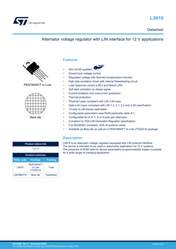
L9918DatasheetAlternator voltage regulator with LIN interface for 12 V applicationsFeaturesPENTAWATT In LineBare dieGADG1604191311PS AEC-Q100 qualifiedClosed loop voltage controlRegulated voltage with thermal compensation functionHigh side excitation driver with internal freewheeling circuitLoad response control (LRC) and Return LRCSelf-start activation by phase signalCurrent limitation and overcurrent protectionThermal protectionPhysical Layer compliant with LIN 2.2A spec.Data Link Layer compliant with LIN 1.3, 2.1, 2.2 and 2.2A specification13 sets of LIN frames selectableConfigurable parameters (see NVM parameter table A1)Configurable for 5, 6, 7, 8 or 9 pole pair alternatorCompliant to VDA LIN-Generator-Regulator specificationFull ISO26262 compliant, ASIL-B systems readyAvailable as Bare die as well as in PENTAWATT In Line (TO220-5) packageDescriptionL9918 is an alternator voltage regulator equipped with LIN protocol interface.The device is intended to be used in automotive application for 12 V systems.The presence of NVM cells for device parameters programmability makes it suitablefor a wide range of charging application.Product status linkL9918Product summaryOrder codePackagePackingL9918PENTAWATTIn Line(TO220-5)TubeL9918BDTRBare dieTape&ReelDS13000 - Rev 2 - September 2022For further information contact your local STMicroelectronics sales office.www.st.com
L9918Functional description1Functional descriptionThe device is an alternator voltage regulator suited for 12 V system, able to communicate with ECU through LINcommunication protocol.The device is housed into an alternator brush holder and it provides current to the excitation coil of the alternator(rotor) through a high side power MOSFET driver. The device is suitable for alternators with different poles pairnumber. An active freewheeling circuit is also integrated into the device.Target function of the device is to modulate the rotor current in order to keep the voltage on car loads steady to atarget value (set point), whatever the vehicle demand.The set point target is typically commanded by the ECU and it is achieved using an internal voltage reference. Setpoint is communicated along with many others functional parameters during the regular device functioning.Slew rate control in combination with external filtering of the interface lines helps to realize electromagneticcompatibility.Figure 1. Simplified application diagramC1B otorFieldratoStorEXCBatteryGNDRegulatorExternal component requiredThe capacitors C1 (2.2 μF ceramic suggested) and C2 (220 pF suggested) to suppress radio frequency injectionhave to be connected as close as possible between the related pin and GND.DS13000 - Rev 2page 2/109
L9918Pin description1.2Pin descriptionFigure 2. Pins connection diagram (top view)5PH4LIN3GND2B 1EXCGADG1604191525PSTable 1. Pin description1.2.1N PINFunction1EXCHigh side driver output to control the rotor current2B Device power supply and Battery voltage sensing3GND4LINCommunication terminal5PHPhase sense inputRegulator groundEXCThis pin is connected to the excitation coil (rotor) of the alternator. The IC supplies a current to the rotor in order tocontrol the output current of the alternator when car load or car speed varies. Device target is to maintain batteryvoltage at defined set point. Inside the device is also embedded a freewheeling circuit, needed to discharge therotor current when the High Side power is turned OFF.1.2.2B The device is supplied by this pin. This voltage is also used as feedback voltage by the regulation loop.1.2.3GNDThe device has one GND pin.1.2.4LINThis LIN pin represents the single-wire bus transmitter and receiver. It is suited for automotive bus systems and isbased on LIN protocol defined in LIN bus specification v1.3, v2.1, v2.2 and v2.2A.1.2.5PHThis pin is connected to one of the stator windings. Its input signal is used for rotor speed measurement, statorvoltage monitoring as well as self-start detection. During the regulation, phase signal voltage level is continuouslymonitored. Phase regulation function is activated if phase amplitude is not addressing desired levels.1.3List of device featuresThe device is designed to satisfy the below features:1.3.1Standby currentWhen L9918 is in standby state, the average power consumption is very low over all temperatures. Currentconsumption can slightly increase while the device is evaluating wakeup sources: device perform a partial wakeup in order to check if eventual signals on phase or LIN pin are valid wakeup events. However even during thispartial wakeup, current consumption remains well below the wakeup state consumption.DS13000 - Rev 2page 3/109
L9918List of device features1.3.2Closed loop voltage controlL9918 regulates the voltage on car loads by closed loop control. Target voltage (set point) can be chosen bydefault (UR DEF REG NVM bits) or it can be sent by the Engine Control Unit (ECU) through LIN interface(VBSPLINRG).1.3.3Load response control (LRC)The torque applied to the engine by the alternator is proportional to the alternator output current. If an electricalload is applied by vehicle harness, the torque applied to the engine can be too high to be sustained, especially ifengine is running at low RPM. The LRC is intended to manage temporarily the alternator output current variationin order to limit torque demand variation.On high rotational speeds, engines do not suffer from torque changes. For this reason load response is switchedoff for RPM SPLRC,x such that any DC adjustment is executed immediately. The load response function will beactive again if RPM SPLRC,x condition is detected.The LRC can be configured by ECU via LIN or it can adopt a default configuration (NVM programming).To avoid permanent voltage adjustment with load response control (while RPM SPLRC,x), even in case of smallduty cycle variations, the regulator has a "blind-zone" range. If duty cycle variation falls within this range, LRC isnot activated. Blind zone control can be programmed by TV SPRUNG NVM bits.The blind zone can be switched through LIN RX frame. This feature can be enabled or disabled by programmingTV SPRUNG EN NVM bit. In case the feature is disabled (TV SPRUNG EN 0) the regulator applies aprogrammed default value: blind zone can’t be changed via LIN and commands corresponding to BZ change intothe RX frames are ignored.1.3.4Pre-excitationConditions for pre-excitation are defined in the internal state machine. In pre-excitation mode, the rotor ismagnetized with a fixed duty cycle in order to produce an induced voltage as soon as the engine turns on.Device behavior in pre-excitation is highly configurable. More detailed explanation on all the possible preexcitation modes are provided in Section 4.2.3 Pre-excitation specific mode selection1.3.5Phase regulationWhen the engine rotates and the device is regulating, the regulator requires a minimum voltage level on the statorcoil signal (phase signal) in order to be ready for engine rotation speed measurement. Proper phase signal levelis guaranteed by phase regulation function (Section 3.2.2 Phase regulation).1.3.6Low voltage functionWhen very low battery voltage is measured, current provided to the excitation coil is driven forcing excitation dutycycle at 100% until a minimum defined voltage is achieved (Section 2.2.4 UV/OV management).1.3.7Overvoltage safety functionL9918 implements an EXC switch off safety function in case of overvoltage detection (Section 2.2.4 UV/OVmanagement).1.3.8Overvoltage functionOther than Overvoltage safety function, L9918 is equipped with a further overvoltage function, which allows filtertime and threshold programmability (Section 2.2.4 UV/OV management).1.3.9Excitation current measurementsDevice is equipped with a current sensor in order to measure the current flowing out from EXC pin(Section 4.2.6 Excitation current measurement).1.3.10Current limitation and overcurrent protectionCurrent limitation can be used to limit the EXC current. Current limitation activation threshold can be set by LIN orby specific NVM bits programming.DS13000 - Rev 2page 4/109
L9918List of device featuresOvercurrent protection is an independent protection which command the shutdown of EXC power stage in case amaximum current threshold is overcame (Section 4.2.6 Excitation current measurement).1.3.11Temperature measurementsA temperature sensor monitors the junction temperature of the regulator. The tolerance is 10 C.1.3.12High temperature voltage limitationL9918 implements a thermal compensation function in order to protect EXC field driver against high temperature(Section 2.2.3 Thermal compensation).1.3.13Self-startThe regulator can be activated even in case of failed or not activated LIN communication. After the self-start, theregulator performs as a multifunction stand-alone regulator with default parameters.1.3.14Non volatile memory (NVM)L9918 contains an NVM memory with a high number of programmable bits. This allows users to apply manydifferent configurations in order to address a wide range of applicative scenarios. NVM programming is operatedby LIN communication through a specific “programming mode procedure” and it is typically done at the end ofproduction line. NVM can be programmed 16 times at most.1.3.15Local interconnect network (LIN) interfaceThe regulator has a bidirectional serial data LIN interface to communicate with the Engine Control Unit (ECU).The Physical Layer is compliant with LIN 2.2A specification. The Data Link Layer is compliant with LIN 1.3, 2.1,2.2 and 2.2A LIN specifications.LIN configuration addresses following functions: Control of the set-point voltage regulation Control of LRC parameters (rise time, LRC disable speed, blind zone) Setting of the excitation current limitation Excitation duty cycle feedback Excitation current feedback High temperature feedback Diagnosis information feedback (LIN error and alternator failure detection) Alternator supplier code feedback Alternator class code feedback Chip supplier identification Chip identification1.3.16Compatibility with different alternator typesAll the RPM speed values specified respect 5, 6, 7, 8 or 9 pole pair alternator definition.DS13000 - Rev 2page 5/109
L9918Internal block diagram1.4Internal block diagramFigure 3. Simplified block diagram1.4.1Power suppliesPower Supplies block contains two sub-blocks: the first is always working, even when device is in stand-by state(Stand-by domain); the latter works just when the device is in active states (OFF in stand-by).The first sub-block supplies Phase and LIN interfaces (needed for the wake up function) and the Stand-by digitalblock.The second sub-block provides the analog and digital supplies to the whole device when PH or LIN pins are fedwith a valid signal. It even provides voltage references for all the sigma-delta converters and provides currentsreference as well. This sub-block is not supplied in stand-by state.1.4.2Phase interfaceThe task of this block is to detect activity on phase pin and verify if the phase signal voltage levels are correct.The circuitry in charge of phase activity detection is always supplied in stand-by.1.4.3LIN interfaceThe block controls the LIN bus transmission and reception. The circuitry in charge of LIN bus activity detection issupplied in stand-by as well.1.4.4Stand-by digital blockThe Stand-by digital block manages the information coming from interfaces and, taking into account NVMconfiguration data, eventually generates a wake-up signal.1.4.5Voltage divider & ΣΔ modulator for regulationThe stage has a resistive divider connected to battery and provides the correct signal voltage range to the internalconverter stage. The stage feeds into the digital block a bit-stream converted in a digital code with a proper lowpass filter. The code is managed in the digital block to act the regulation.DS13000 - Rev 2page 6/109
L9918State diagram1.4.6Voltage divider & ΣΔ modulator for overvoltage/undervoltageThe stage has a resistive divider connected to battery (different and independent of the previous stage) andprovides the correct signal voltage range to the internal data converter. The stage feeds into the digital block abit-stream converted in a digital code with a proper low pass filter. The code is managed in the digital block toimplement the overvoltage and under-voltage detections.1.4.7Thermal sensorThermal sensor provides to the digital block the device temperature. The block embeds a thermal sensor and asigma-delta converter whose bit-stream is converted in a digital code.1.4.8OscillatorThe block provides the clock reference for the digital function and the Charge Pump block. The frequency value is16MHz 5%.1.4.9Excitation driverThe block embeds a power N-channel MOS inserted between B and EXC pins and a circuitry that is able todrive it. A freewheeling circuit is inserted between EXC and GND pins, located across the excitation coil forenergy recirculation purpose. The protection against short circuit on EXC pin is also implemented. If a short circuitis detected the excitation current is turned off and the subsequent turn-on attempt is retried at every excitationperiod.A current measurement block provides the excitation current value flowing in the high-side power MOS. In orderto reach the requested accuracy, a dedicated thermal sensor is located close to the current measurement block.Power MOS temperature is used to calibrate the current measure.1.4.10Safety switch OFFSafety Switch OFF is a separate block featured for safety reason. It must switch the field driver power MOS gateoff when a battery overvoltage condition is detected.1.4.11Charge pumpCharge pump is mandatory to supply correctly the excitation power MOS gate.1.4.12Non volatile memory (NVM)The NVM allows to set all configurable device parameters. Please refer to default mode parameter table (seeSection A.1 ).1.4.13Digital blockAll device functions are managed by the digital block. The state diagram is shown in the next chapter.1.5State diagramThe following figure describes L9918 state machine.DS13000 - Rev 2page 7/109
L9918State diagramFigure 4. L9918 finite state machine diagramStandby (*)LIN ActivityPH ActivityN N startWake UpSelf start (N SPss,x )OR hot startLIN COM TOORVBSPLINRG 10.6Safety(EXC OFF)(N Nstart )FAULT OFFPre-ExcitationFAULT ONFAULTOFFFAULTONVBSPLINRG 10.6&&(N Nstart)(N Nstart)VBSPLINRGLINRegulation (**)RegulationDefaultLIN COM TORegulation State1.5.1LIN Sleep Command(LIN TO) OR(PH TO) ORLIN Sleep Command(*) Considered timeout depends on the wakeupsources. If no LIN activity is detected (devicewakeup by phase) device consider PH TO. If LINactivity is detected, adopted timeout is LIN TO,independently of the wakeup event.(**) In case REG AUS 0x1, EXC is disabledwhen VBSPLINRG 10.6.StandbyDevice conditions to enter in stand-by mode: LIN time-out or phase time-out; LIN sleep command.Device considers two different timeouts to go back to standby from wake up: LIN timeout and phase timeout.LIN timeout means: no activity on LIN bus during specified time (see tLIN to parameter).Phase timeout means: no activity on phase signal during a specified time (see tPH to parameter).Standby entrance from Wake Up state can be done accordingly to one of the two timeouts. In case no LIN activityis detected (wake up by phase), device goes in standby if no more PH activity occurs for longer than tPH to.If LIN activity is detected, device transition from Wake Up to Standby uses tLIN to independently of the wake upsource.The standby mode can even be forced by ECU sending LIN sleep command.In stand-by state the device has: No excitation. Duty cycle (DC) on EXC pin is equal to zero. Current consumption aligned to IBstbyL80, IBstbyH80, according to the internal temperature.In this state the device needs a small amount of quiescent current to supply logic, phase detector and LINreceiver only.When device is supplied after a shutdown, as soon as the voltage reaches VBPOR threshold, the digital block incharge of evaluate input coming from PH and LIN pins is initialized. For this reason only B levels higher thanVBPOR can ensure device wakeup functionalities.1.5.2Wake-upThis state is reached from Standby if at least one of the following wake up sources occur: Activity is detected on LIN bus (LIN wakeup event selected by LIN WAKEUP PATTERN NVM bits,accordingly to LIN specification document). Activity on PH pin is detected (VPStartTh).Wake up state can also be accessed from Pre-excitation state in case no valid communication is provided formore than LIN COM timeout (tLIN COM) or in case VBSPLINRG 10.6 is received.DS13000 - Rev 2page 8/109
L9918State diagramDevice remains in wake up state as long as at least one of the listed wake up source is present. If wake upsources are no longer detected, the device goes back in stand-by with a proper time-out.Every time the device enters the wake up state from standby state, an initialization procedure consisting in anNVM download procedure is triggered. Every volatile data so far acquired (i.e. setup commanded through LIN Rxframes) are lost.In wake up state: All the blocks are ON, the current consumption is higher than standby current consumption. The duty cycle on EXC pin is equal to zero. The phase sensitivity is VPStartTh (peak to peak).In case of cranking event, due to low battery voltage value, LIN protocol could not be working. LIN timeout canoccur and the parameters sent by LIN protocol will be lost.One particular behavior related to Wake Up state is the behavior occurring when device detects activity (i.e.TX frames or RX frames with unrecognized ID or checksum) on LIN bus. Once this activity is detected, devicedoesn’t move toward regulation state even if valid PH is present. It keep EXC OFF, waiting for a valid set pointcommand.Phase regulation is active into Wake-up state. It is performed just in case phase rotation greater than Nstart.1.5.3Pre-excitationThe pre-excitation state is reached as soon as VBSPLINRG differs from 10.6 V and the engine rotation is lowerthan Nstart.The purpose of pre-excitation is to increase the alternator magnetization in order to guarantee proper conditionsfor PH signal measurement in case the engine start to rotate. The pre-excitation is done driving the alternatorrotor with a PWM signal that has fixed frequency (fFSWpreexc) and fixed duty cycle (25 %).If the battery voltage is higher than the maximum set-point value selectable by LIN protocol (VB LIM) the dutycycle is reduced to 8 % or to 0 %, depending on NVM bit SST ULIM TV0 EN.In pre-excitation state: LRC function is disabled. Phase regulation is disabled. Current limitation control by LIN disabled except for specific pre-excitation mode (described below). Default EXC current limitation is activated by dedicated NVM bits (IMAX VE and IMAX VE VAL). Safety functions are enabled.Device is even featured with a specific pre-excitation mode, selectable by SV FORD EN NVM bit. When this isenabled, EXC signal behavior depends on B value respect to the set point (VBSPLINRG) and on LIN frame datacarried by the LIN RX frame.More detailed explanations and examples on special mode can be found in Section 4.2.3 Pre-excitation specificmode selection.1.5.4Regulation mode1.5.4.1LIN regulation modeThis state can be reached: from pre-excitation state when alternator rotation is higher than Nstart; fromRegulation default state when valid set-point (VBSPLINRG 10.6 V) is provided.In particular, more detailed explanations must be dedicated to the last of these cases (LIN Regulation enteredfrom Regulation Default). If the Regulation Default state persists for more than LIN TO, two frames are neededto enter the LIN Regulation mode: the first one to wake up the LIN block, the second one to communicate LINregulation data. On the other hand, if Default Regulation persist for less than LIN TO, the device is ready toreceipt LIN regulation information by a single LIN RX frame. In such case LIN Regulation mode can be enteredsending just one RX frame.In this state the device modulates the EXC output current in order to set the battery line voltage to the LIN setpoint (VBSPLINRG).In LIN regulation mode state: LRC function enabled accordingly to LIN communication. Phase regulation enabled.DS13000 - Rev 2page 9/109
L9918State diagram 1.5.5Current limitation enabled accordingly to current limitation thresholds provided by LIN or by NVM registerscontents (the lower between the two current limitation thresholds is adopted).Safety functions active.Thermal compensation enabled.Low voltage function.Regulation defaultThis mode is equivalent to the LIN regulation mode except that, being without LIN communication, NVM defaultregulation parameters (VBSPDEF, TFLRCup, TFLRCdw, SPLRC) are used for regulation.Regulation default can be entered from wake-up state when phase rotation is greater than SPSS (N NOTSTARTNVM register). Phase amplitude required to enter regulation default depends on KLV AC ADAP MIN NOT,KLV AC ADAP MIN and ACADAPMIN MODE NVM registers.Regulation default can be entered from LIN regulation state in case no valid frame is provided for a time longerthan tLIN COM, adopted set point changes from VBSPLINRG to VBSPDEF.Set point transition to default VBSPDEF is performed with a ramp of VBSP LDslope and excitation currentlimitation moves to IFELD MAXB or I MAX with a ramp of IFLIM LDslope.If LIN communication resumes, regulation voltage and current limitation target change immediately, accordingly tothe received RX frame data.In regulation default state: LRC function enabled accordingly with NVM selection. Phase regulation enabled. Current limitation set to IFELD MAXB and I MAX. Safety function enabled. Thermal compensation enabled. Low voltage function.1.5.6SafetySafety state is an excitation OFF state which is entered as soon as a safety protection mechanism is activatedwhile device is into pre-excitation or regulation state.Here below a list of the safety mechanisms implemented by L9918:1.5.6.1Current protectionIn all the states where the excitation power MOS is active, overcurrent protection function is working. As soon asthe IFOCP threshold is reached the power is switched OFF.1.5.6.2Thermal protectionIn case TJ reaches the Tsd,x threshold (selectable by NVM bits THERMAL TH SEL), EXC power MOS isswitched OFF till the TJ temperature decrease below Tsd,x - Tsdhy.1.5.6.3Overvoltage safety protectionIn case of B VBOV safetyL for more than TOVflt safetyL or B VBOV safetyH for more than TOVflt safetyH, EXCpower MOS is switched OFF till B returns at a value lower than VBOV safetyL for more than TOVflt safetyL time.DS13000 - Rev 2page 10/109
L9918Product characteristics1.6Product characteristics1.6.1Absolute maximum ratingsTable 2. Absolute maximum LDTransient supply voltage (load dump) t 400 msVclVIBondDC pin current on EXC, B , GND(bonding limitation)15A-88kVESDHBMESD HBM (All pins vs.GND) R 1.5kΩ,C 100pF, RT 25 CESDCDMESD CDM on EXC and PH pins-750750VESDCDMESD CDM on B and LIN pins-500500VInternal clamping structureTable 3. Internal clamping structureSymbolVclVcl LIN1.6.3ParameterNotesMin.Typ.Max.UnitInternal centralclamp voltageB current injected I 20mA5864VDedicated Clamp toLIN pinCurrent injected in LIN pin I 20mA40-VPIN number - absolute maximum ratings - operative rangeTable 4. PIN number - absolute maximum ratings - operative rangen.Pin1ABS max ratingoperative rangeUnitMin.Max.Min.Max.EXC-2B - 1.6B V2B -0.3(1)-Vcl(3)618V3GND----LIN-27(2),(3)Vcl LIN-318VPH-27(2)Vcl-318V451. 3.2 V, transient 5 s.2. Value at cold temperature: -25 V.3. LIN and B AMR not valid at the same time.1.6.4Thermal dataTable 5. Thermal dataSymbolRth j-caseDS13000 - Rev 2ParameterThermal resistance junction-tocaseNotesRelated to TO220Min.Typ.Max.Unit2 C/Wpage 11/109
L9918Product Thermal shutdown thresholdTemperature to disable EXCdriver for chip protection (set byTHERMAL TH SEL)Tsd,4TsdhyThermal shut-down hysteresisTyp.Max.Unit170180190 C165175185 C175185195 C180190200 C2610 CTemp RTj for full functional and full spec-40150 CTemp FTj for full functional withparameters deviation150190 C145 CTemp SRctrlCurrent SR disable temperatureTemp SRctrl hiTemp SRctrl hysteresisstTstg, TcaseDS13000 - Rev 2EXC from OFF STATE (due tothermal shutdown) to ON STATEMin.Storage and case temperaturerangeTj over which EXC currentslew rate control is disabled(SR HT DIS)125Hysteresis from “disabled”state (entered becauseTj Temp SRctrl) to “enabled”state1356-40 C150 Cpage 12/109
L9918Power supply and battery voltage sensing - B pin2Power supply and battery voltage sensing - B pinUnless otherwise specified, all the electrical characteristics provided in this chapter refers to Tj between -40 Cand 150 C.2.1B electrical characteristicTable 6. B electrical 618VVBOpVROperating Voltage RangeVBdeepLVDeep low Voltage Rangeparameter degradation, not reset(according to ISO16750 - cranking )36VIBstbyL80Stand-by current consumptionlower 80 CVB 12.5 V; VPH 0;VLIN 12.5 V; T 80 C150µAIBstbyH80Stand-by current consumptionhigher 80 CVB 12.5 V; VPH 0;VLIN 12.5 V; T 80 C1100µACurrent consumption out of standbyVB 12.5 V; No current load onEXC and LIN30mASet-Point Voltage Range for LINcommunicationVPH 10 Vpp square wave at500 Hz; valid LIN communication;@ Tj 30 C10.616VVPH 10 Vpp square wave at500 Hz; no LIN communication; @Tj 30 C10.616VSet Point voltage toleranceTj 30 CVPH 10 Vpp square waveat 500 Hz; with/without LINcommunication (please refer toFigure 5)-1000 100mVSet Point VoltageTolerance-40 C Tj 150 CVPH 10 Vpp square waveat 500 Hz; with/without LINcommunication ((please refer toFigure 5)-1500 150mVΔVBloadRegulated Voltage variation withthe loadDifference between regulatedvoltage when EXC duty cycle is10 % and regulated voltage whenEXC duty cycle is 90 %I ANT/P ANTVΔVBspeed(1)Regulated Voltage variation withthe speedDifference between regulatedvoltage when Ialt 10 A;2000rpm Alt speed 18000rpm100mVVBSP LDslopeVoltage Slope to address defaultSet Point starting from LIN SetPoint0.22V/sIBactiveVBSPLINRGVBSPDEFDefault Set Point Voltage Range(no LIN communication)(NVM UR DEF REG)VBSP tol30VBSP tolTrange18-500.180.21. Not subject to production test, specified by design (alternator dependent).The maximum tolerated ripple value on B is 6 V whatever speed and load. In case voltage ripple on batteryline exceeds this limit, declared tolerance cannot be guaranteed,DS13000 - Rev 2page 13/109
L9918B electrical characteristicFigure 5. Set point voltage tolerance versus temperature: example with 14V set point (VBSPLINRG orVBSPDEF).Setpoint emperature8090100110120130140150Table 7. Over and under voltage ge function threshold(U FELD rectional Over-voltage filtertime (U FELD AUS TIME)VBOVft,4µs780µs1040µs0µsVBOV safetyLOver-voltage for safety lowthreshold16.51717.5VVBOV safetyHOver-voltage for safety highthreshold17.51818.5VTOVflt safetyLOver-voltage filter time for safetylow thresholdTOVflt safetyHOver-voltage filter time for safetyhigh .2510.510.75VVLOW,3VLOW,4DS13000 - Rev 2520Low-Voltage threshold(U FELD EIN)page 14/109
L9918B characteristicsSymbolVLOW,7VLOW,8VB LIMParameterLow-Voltage threshold(U FELD EIN)NotesMin.Typ.Max.Unit10.751111.25VVLOW 9.9 V 0.388 * (VSET 10.6 V)Set point limit thresholdVBLVft,1VBLVft,2VBLVft,3Bidirectional Low-voltage filtertime (U FELD EIN TIME)VBLVft,4VBPORPower On Reset when is elapsedat least td timetdMax battery interruption timet1Minimum time between twobattery interruptions2.2B characteristics2.2.1Set point value 0µsmsIt is possible for the customer at end of line to perform a set-point voltage value correction by dedicated NVM bits(UR OFFSET). The set-point voltage value can be adjusted from - 200 mV to 150 mV with steps of 50 mV. Suchvoltage correction applies both to default set point (VBSPDEF) and LIN set point (VBSPLINRG).2.2.2Voltage regulation loopRegulation loop circuit is composed by two main blocks: direct (or proportional) control block and feedback (ordeviation) control block.Direct or proportional control applies an EXC DC correction which directly depends on the calculated error (whichis obtained as B - VBSPLINRG/VBSPDEF).Proportional control can be selected by P ANT NVM bits. Small values of P ANT correspond to a high regulationsensitivity.Figure 6 (P ANT regulation) reports the output voltage (B ) variation depending in the EXC DC in case onlyproportional regulation is used.Feedback (or deviation) control is a set point correction which depends on EXC DC.Such correction shall be used in order to compensate eventual voltage drop occurring between car battery andcar loads and regulator B .Feedback control options can be selected by I ANT NVM bits. High values of I ANT correspond to a high offseton the adopted set point. I ANT offset is applied after a filter time selectable by I FILT NVM bits.Figure 6 (I ANT variation) reports the dependency between EXC DC and B for various I ANT settings.DS13000 - Rev 2page 15/109
L9918B characteristicsFigure 6. Dependency between B and EXC duty cycle in case of P ANT regulation and I ANT variationAlternatoroutput voltageEXC DCSet point – P ANTI ANT 0 mVSet point100%Set point –P ANT200 mVI ANSet point – 200mV50%Set point0%I ANTSet point – P ANTB P ANT regul
REC_PDF)) (internal timing, from physical layer to data layer logic) 6 μs t. rx_sym. Symmetry of receiver propagation delay rising edge w.r.t. falling edge (T. RX_SYM t. REC_PDF - t. REC_PDR) -2 2 μs LIN. autobaud_range. Baud rate selection on transceiver Automatic selection of one of the baud rate slots 1 20 kHz t. LIN_COM. LIN COM timeout .
