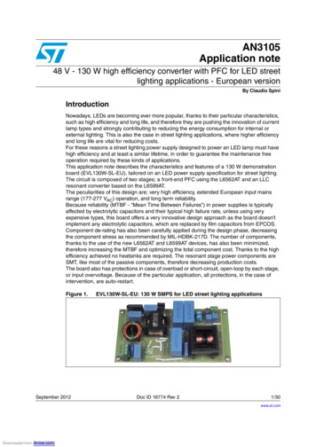
Transcription
Is Now Part ofTo learn more about ON Semiconductor, please visit our website atwww.onsemi.comPlease note: As part of the Fairchild Semiconductor integration, some of the Fairchild orderable part numberswill need to change in order to meet ON Semiconductor’s system requirements. Since the ON Semiconductorproduct management systems do not have the ability to manage part nomenclature that utilizes an underscore( ), the underscore ( ) in the Fairchild part numbers will be changed to a dash (-). This document may containdevice numbers with an underscore ( ). Please check the ON Semiconductor website to verify the updateddevice numbers. The most current and up-to-date ordering information can be found at www.onsemi.com. Pleaseemail any questions regarding the system integration to Fairchild questions@onsemi.com.ON Semiconductor and the ON Semiconductor logo are trademarks of Semiconductor Components Industries, LLC dba ON Semiconductor or its subsidiaries in the United States and/or other countries. ON Semiconductor owns the rights to a numberof patents, trademarks, copyrights, trade secrets, and other intellectual property. A listing of ON Semiconductor’s product/patent coverage may be accessed at www.onsemi.com/site/pdf/Patent-Marking.pdf. ON Semiconductor reserves the rightto make changes without further notice to any products herein. ON Semiconductor makes no warranty, representation or guarantee regarding the suitability of its products for any particular purpose, nor does ON Semiconductor assume any liabilityarising out of the application or use of any product or circuit, and specifically disclaims any and all liability, including without limitation special, consequential or incidental damages. Buyer is responsible for its products and applications using ONSemiconductor products, including compliance with all laws, regulations and safety requirements or standards, regardless of any support or applications information provided by ON Semiconductor. “Typical” parameters which may be provided in ONSemiconductor data sheets and/or specifications can and do vary in different applications and actual performance may vary over time. All operating parameters, including “Typicals” must be validated for each customer application by customer’stechnical experts. ON Semiconductor does not convey any license under its patent rights nor the rights of others. ON Semiconductor products are not designed, intended, or authorized for use as a critical component in life support systems or any FDAClass 3 medical devices or medical devices with a same or similar classification in a foreign jurisdiction or any devices intended for implantation in the human body. Should Buyer purchase or use ON Semiconductor products for any such unintendedor unauthorized application, Buyer shall indemnify and hold ON Semiconductor and its officers, employees, subsidiaries, affiliates, and distributors harmless against all claims, costs, damages, and expenses, and reasonable attorney fees arising outof, directly or indirectly, any claim of personal injury or death associated with such unintended or unauthorized use, even if such claim alleges that ON Semiconductor was negligent regarding the design or manufacture of the part. ON Semiconductoris an Equal Opportunity/Affirmative Action Employer. This literature is subject to all applicable copyright laws and is not for resale in any manner.Downloaded from Arrow.com.
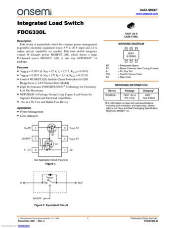
FDMC8200Dual N-Channel PowerTrench MOSFET30 V, 9.5 mΩ and 20 mΩFeaturesGeneral DescriptionQ1: N-ChannelThis device includes two specialized N-Channel MOSFETs in a Max rDS(on) 20 mΩ at VGS 10 V, ID 6 Adual Power33 (3mm x 3mm MLP) package. The switch nodehas been internally connected to enable easy placement and Max rDS(on) 32 mΩ at VGS 4.5 V, ID 5 Arouting of synchronous buck converters.The controlQ2: N-ChannelMOSFET (Q1) and synchronous MOSFET (Q2) have been Max rDS(on) 9.5 mΩ at VGS 10 V, ID 9 Adesigned to provide optimal power efficiency. Max rDS(on) 13.5 mΩ at VGS 4.5 V, ID 7 AApplications RoHS Compliant Mobile Computing Mobile Internet Devices General Purpose Point of LoadPin 1G1D1D1D1V INV ING HSD1D2/S1G2V INV INITCSWS2S2HNS2G TTOMPower 33MOSFET Maximum Ratings TC 25 C unless otherwise notedSymbolVDSDrain to Source VoltageParameterVGSGate to Source VoltageDrain Current - Continuous (Package limited)Q130Q230UnitsV(Note 3) 20 20VTC 25 C1818- Continuous (Silicon limited)TC 25 C2345- ContinuousTA 25 C8 1a12 1b4040Power DissipationTA 25 C1.9 1a2.2 1bPower DissipationTA 25 C0.7 1c0.9 1dID- PulsedPDTJ, TSTGOperating and Storage Junction Temperature Range-55 to 150AW CThermal CharacteristicsRθJA65 1aThermal Resistance, Junction to AmbientRθJAThermal Resistance, Junction to AmbientRθJCThermal Resistance, Junction to Case1801c7.555 1b145 1d C/W4Package Marking and Ordering InformationDevice MarkingFDMC8200DeviceFDMC8200 2009 Fairchild Semiconductor CorporationFDMC8200 Rev.A2Downloaded from Arrow.com.PackagePower 331Reel Size13 ”Tape Width12 mmQuantity3000 unitswww.fairchildsemi.comFDMC8200 Dual N-Channel PowerTrench MOSFETJune 2014
SymbolParameterTest ConditionsTypeMin3030TypMaxUnitsOff CharacteristicsBVDSSDrain to Source Breakdown VoltageID 250 μA, VGS 0 VID 250 μA, VGS 0 VQ1Q2ΔBVDSSΔTJBreakdown Voltage TemperatureCoefficientID 250 μA, referenced to 25 CID 250 μA, referenced to 25 CQ1Q2IDSSZero Gate Voltage Drain CurrentVDS 24 V, VGS 0 VVDS 24 V, VGS 0 VQ1Q211μAIGSSGate to Source Leakage CurrentVDS 20 V, VGS 0 VQ1Q2100100nAnA3.03.0VV1414mV/ COn CharacteristicsVGS(th)Gate to Source Threshold VoltageVGS VDS, ID 250 μAVGS VDS, ID 250 μAQ1Q2ΔVGS(th)ΔTJGate to Source Threshold VoltageTemperature CoefficientID 250 μA, referenced to 25 CID 250 μA, referenced to 25 CQ1Q2-5-6VGS 10 V, ID 6 AVGS 4.5 V, ID 5 AVGS 10 V, ID 6 A, TJ 125 CQ1162422203228VGS 10 V, ID 9 AVGS 4.5 V, ID 7 AVGS 10 V, ID 9 A, TJ 125 CQ27.39.5109.513.513VDD 5 V, ID 6 AVDD 5 V, ID 9 5pFrDS(on)gFSStatic Drain to Source On ResistanceForward Transconductance1.01.02.32.3mV/ CmΩSDynamic CharacteristicsCissInput CapacitanceCossOutput CapacitanceCrssReverse Transfer CapacitanceQ1Q22030RgGate .310nCQ1Q21.84.1nCQ1Q211.5nCVDS 15 V, VGS 0 V, f 1 MHZΩSwitching Characteristicstd(on)Turn-On Delay TimetrRise Timetd(off)Turn-Off Delay TimetfFall TimeQg(TOT)Total Gate ChargeQg(TOT)Total Gate ChargeQgsGate to Source ChargeQgdGate to Drain “Miller” Charge 2009 Fairchild Semiconductor CorporationFDMC8200 Rev.A2Downloaded from Arrow.com.Q1VDD 15 V, ID 1 A,VGS 10 V, RGEN 6 ΩQ2VDD 15 V, ID 1 A,VGS 10 V, RGEN 6 ΩVGS 0 V to 10 V Q1:VDD 15 V,VGS 0 V to 4.5 V ID 6 A,Q2:VDD 15 V,ID 9 A,2www.fairchildsemi.comFDMC8200 Dual N-Channel PowerTrench MOSFETElectrical Characteristics TJ 25 C unless otherwise noted
SymbolParameterTest 3212434nsQ1Q22.35.61012nCDrain-Source Diode CharacteristicsVSDSource to Drain Diode Forward VoltageVGS 0 V, IS 6 AVGS 0 V, IS 9 AtrrReverse Recovery TimeQrrReverse Recovery ChargeQ1IF 6 A, di/dt 100 A/sQ2IF 9 A, di/dt 100 A/s(Note 2)(Note 2)Notes:1. RθJA is determined with the device mounted on a 1in2 pad 2 oz copper pad on a 1.5 x 1.5 in. board of FR-4 material. RθJC is guaranteed by design while RθCA is determinedby the user's board design.a.65 C/W when mounted ona 1 in2 pad of 2 oz copperb.55 C/W when mounted ona 1 in2 pad of 2 oz copperc. 180 C/W when mounted on aminimum pad of 2 oz copperd. 145 C/W when mounted on aminimum pad of 2 oz copper2. Pulse Test: Pulse Width 300 μs, Duty cycle 2.0%.3. As an N-ch device, the negative Vgs rating is for low duty cycle pulse ocurrence only. No continuous rating is implied. 2009 Fairchild Semiconductor CorporationFDMC8200 Rev.A2Downloaded from Arrow.com.3www.fairchildsemi.comFDMC8200 Dual N-Channel PowerTrench MOSFETElectrical Characteristics TJ 25 C unless otherwise noted
404ID, DRAIN CURRENT (A)VGS 6 V30VGS 4.5 V20VGS 4 V10PULSE DURATION 80 μsDUTY CYCLE 0.5% MAXVGS 3.5 V00.00.51.01.52.02.5PULSE DURATION 80 μsDUTY CYCLE 0.5% MAXNORMALIZEDDRAIN TO SOURCE ON-RESISTANCEVGS 10 V3VGS 3.5 VVGS 4 V2VGS 4.5 V103.0010VDS, DRAIN TO SOURCE VOLTAGE (V)40100ID 6 AVGS 10 VrDS(on), DRAIN TO1.41.21.00.8-75-50SOURCE ON-RESISTANCE (mΩ)NORMALIZEDDRAIN TO SOURCE ON-RESISTANCE30Figure 2. Normalized On-Resistancevs Drain Current and Gate Voltage1.6PULSE DURATION 80 μsDUTY CYCLE 0.5% MAX80ID 6 A60TJ 125 oC4020TJ 25 oC0-25025 50 75 100 125 150TJ, JUNCTION TEMPERATURE (oC)246810VGS, GATE TO SOURCE VOLTAGE (V)Figure 3. Normalized On Resistancevs Junction TemperatureFigure 4. On-Resistance vs Gate toSource Voltage4040IS, REVERSE DRAIN CURRENT (A)PULSE DURATION 80 μsDUTY CYCLE 0.5% MAXID, DRAIN CURRENT (A)20ID, DRAIN CURRENT (A)Figure 1. On Region Characteristics30VDS 5 V20TJ 150 oCTJ 25 oC10TJ -55 oC02.02.53.03.54.01TJ 150 oC0.1TJ 25 oC0.01TJ -55 oC0.40.60.81.01.2VSD, BODY DIODE FORWARD VOLTAGE (V)Figure 5. Transfer Characteristics 2009 Fairchild Semiconductor CorporationFDMC8200 Rev.A2VGS 0 V100.0010.24.5VGS, GATE TO SOURCE VOLTAGE (V)Downloaded from Arrow.com.VGS 10 VVGS 6 VFigure 6. Source to Drain DiodeForward Voltage vs Source Current4www.fairchildsemi.comFDMC8200 Dual N-Channel PowerTrench MOSFETTypical Characteristics (Q1 N-Channel) TJ 25 C unless otherwise noted
101000VGS, GATE TO SOURCE VOLTAGE (V)ID 6 ACissCAPACITANCE (pF)8VDD 20 VVDD 15 V6VDD 10 V4Coss100Crss2f 1 MHzVGS 0 V00246100.1811030VDS, DRAIN TO SOURCE VOLTAGE (V)Qg, GATE CHARGE (nC)Figure 7. Gate Charge CharacteristicsFigure 8. Capacitance vs Drainto Source Voltage10025o10ID, DRAIN CURRENT (A)I D , DRAIN CURRENT (A)RθJC 7.5 C/W100 us1 ms110 ms100 msTHIS AREA ISLIMITED BY rDS(on)0.11s10 sDCSINGLE PULSETJ MAX RATEDRθJA 180 o C/W0.0120VGS 10 V15Limited by Package10VGS 4.5 V5oTA 25 C0.0010.010.11100251002005075100125150oTc, CASE TEMPERATURE ( C)VDS, DRAIN to SOURCE VOLTAGE (V)Figure 9. Forward Bias SafeOperating AreaFigure 10. Maximum Continuous Drain Currentvs Case TemperatureP(PK), PEAK TRANSIENT POWER (W)300VGS 10 V100SINGLE PULSEoRθJA 180 C/WoTA 25 C1010.5-410-310-210-1101101001000t, PULSE WIDTH (s)Figure 11. Single Pulse Maximum Power Dissipation 2009 Fairchild Semiconductor CorporationFDMC8200 Rev.A2Downloaded from Arrow.com.5www.fairchildsemi.comFDMC8200 Dual N-Channel PowerTrench MOSFETTypical Characteristics (Q1 N-Channel) TJ 25 C unless otherwise noted
2NORMALIZED THERMALIMPEDANCE, ZθJA10.1DUTY CYCLE-DESCENDING ORDERD 0.50.20.10.050.020.01PDMt1t2NOTES:DUTY FACTOR: D t1/t2PEAK TJ PDM x ZθJA x RθJA TASINGLE PULSE0.01oRθJA 180 C/W0.003-410-310-210-1101101001000t, RECTANGULAR PULSE DURATION (sec)Figure 12. Junction-to-Ambient Transient Thermal Response Curve 2009 Fairchild Semiconductor CorporationFDMC8200 Rev.A2Downloaded from Arrow.com.6www.fairchildsemi.comFDMC8200 Dual N-Channel PowerTrench MOSFETTypical Characteristics (Q1 N-Channel) TJ 25 C unless otherwise noted
406NORMALIZEDDRAIN TO SOURCE ON-RESISTANCEID, DRAIN CURRENT (A)VGS 10 V30VGS 4.5 VVGS 4 V20VGS 3.5 V1000.0PULSE DURATION 80 μsDUTY CYCLE 0.5% MAXVGS 3 V0.51.01.52.02.5PULSE DURATION 80 μsDUTY CYCLE 0.5% MAX5VGS 3 V4VGS 3.5 V3VGS 4 V21VGS 10 V03.0010VDS, DRAIN TO SOURCE VOLTAGE (V)4060ID 9 AVGS 10 VrDS(on), DRAIN TO1.41.21.00.80.6-75-50-250255075SOURCE ON-RESISTANCE (mΩ)NORMALIZEDDRAIN TO SOURCE ON-RESISTANCE30Figure 14. Normalized on-Resistance vs DrainCurrent and Gate Voltage1.6PULSE DURATION 80 μsDUTY CYCLE 0.5% MAX50ID 9 A403020TJ 125 oC10TJ 25 oC0100 125 1502TJ, JUNCTION TEMPERATURE (oC)46810VGS, GATE TO SOURCE VOLTAGE (V)Figure 16. On-Resistance vs Gate toSource VoltageFigure 15. Normalized On-Resistancevs Junction Temperature40IS, REVERSE DRAIN CURRENT (A)40PULSE DURATION 80 μsDUTY CYCLE 0.5% MAXID, DRAIN CURRENT (A)20ID, DRAIN CURRENT (A)Figure 13. On-Region Characteristics30VDS 5 V20TJ 150 oCTJ 25 oC10TJ -55 oC01.52.02.53.03.5TJ 150 oC1TJ 25 oC0.10.01TJ -55 oC0.20.40.60.81.01.2VSD, BODY DIODE FORWARD VOLTAGE (V)Figure 18. Source to Drain DiodeForward Voltage vs Source CurrentFigure 17. Transfer Characteristics 2009 Fairchild Semiconductor CorporationFDMC8200 Rev.A2VGS 0 V100.0010.04.0VGS, GATE TO SOURCE VOLTAGE (V)Downloaded from Arrow.com.VGS 4.5 V7www.fairchildsemi.comFDMC8200 Dual N-Channel PowerTrench MOSFETTypical Characteristics (Q2 N-Channel) TJ 25 C unless otherwise noted
2000CissID 9 A10008VDD 15 VCAPACITANCE (pF)VGS, GATE TO SOURCE VOLTAGE (V)106VDD 10 VVDD 20 V4Coss100Crss2f 1 MHzVGS 0 V003691215100.11811030VDS, DRAIN TO SOURCE VOLTAGE (V)Qg, GATE CHARGE (nC)Figure 19. Gate Charge CharacteristicsFigure 20. Capacitance vs Drainto Source Voltage10050oRθJC 4 C/W100 us10ID, DRAIN CURRENT (A)I D , DRAIN CURRENT (A)VGS 10 V1 ms1THIS AREA ISLIMITED BY r DS(on)10 ms100 msSINGLE PULSETJ MAX RATED0.11sRθJA 145 oC/W10 sDCTA 25 oC0.010.010.11104030VGS 4.5 V2010025100200Limited by Package5075100125150oTc, CASE TEMPERATURE ( C)VDS, DRAIN to SOURCE VOLTAGE (V)Figure 21. Forward Bias SafeOperating AreaFigure 22. Maximum Continuous DrainCurrent vs Case TemperatureP(PK), PEAK TRANSIENT POWER (W)1000VGS 10 VSINGLE PULSEoRθJA 145 C/WoTA 25 C1001010.5-410-310-210-1101101001000t, PULSE WIDTH (s)Figure 22. Single Pulse Maximum Power Dissipation 2009 Fairchild Semiconductor CorporationFDMC8200 Rev.A2Downloaded from Arrow.com.8www.fairchildsemi.comFDMC8200 Dual N-Channel PowerTrench MOSFETTypical Characteristics (Q2 N-Channel) TJ 25 C unless otherwise noted
2NORMALIZED THERMALIMPEDANCE, ZθJA10.1DUTY CYCLE-DESCENDING ORDERD 0.50.20.10.050.020.01PDMt1t20.01NOTES:DUTY FACTOR: D t1/t2PEAK TJ PDM x ZθJA x RθJA TASINGLE PULSEoRθJA 145 C/W0.001-410-310-210-1101101001000t, RECTANGULAR PULSE DURATION (sec)Figure 23. Junction-to-Ambient Transient Thermal Response Curve 2009 Fairchild Semiconductor CorporationFDMC8200 Rev.A2Downloaded from Arrow.com.9www.fairchildsemi.comFDMC8200 Dual N-Channel PowerTrench MOSFETTypical Characteristics (Q2 N-Channel) TJ 25 C unless otherwise noted
FDMC8200 Dual N-Channel PowerTrench MOSFETDimensional Outline and Pad LayoutPackage drawings are provided as a service to customers considering Fairchild components. Drawings may change in any mannerwithout notice. Please note the revision and/or date on the drawing and contact a Fairchild Semiconductor representative to verify orobtain the most recent revision. Package specifications do not expand the terms of Fairchild’s worldwide terms and conditions, specifically the warranty therein, which covers Fairchild products.Always visit Fairchild Semiconductor’s online packaging area for the most recent package ageDetails.html?id PN MLDED-CX8 2009 Fairchild Semiconductor CorporationFDMC8200 Rev.A2Downloaded from Arrow.com.10www.fairchildsemi.com
tm*Trademarks of System General Corporation, used under license by Fairchild Semiconductor.DISCLAIMERFAIRCHILD SEMICONDUCTOR RESERVES THE RIGHT TO MAKE CHANGES WITHOUT FURTHER NOTICE TO ANY PRODUCTS HEREIN TO IMPROVERELIABILITY, FUNCTION, OR DESIGN. FAIRCHILD DOES NOT ASSUME ANY LIABILITY ARISING OUT OF THE APPLICATION OR USE OF ANYPRODUCT OR CIRCUIT DESCRIBED HEREIN; NEITHER DOES IT CONVEY ANY LICENSE UNDER ITS PATENT RIGHTS, NOR THE RIGHTS OF OTHERS.THESE SPECIFICATIONS DO NOT EXPAND THE TERMS OF FAIRCHILD’S WORLDWIDE TERMS AND CONDITIONS, SPECIFICALLY THE WARRANTYTHEREIN, WHICH COVERS THESE PRODUCTS.LIFE SUPPORT POLICYFAIRCHILD’S PRODUCTS ARE NOT AUTHORIZED FOR USE AS CRITICAL COMPONENTS IN LIFE SUPPORT DEVICES OR SYSTEMS WITHOUT THEEXPRESS WRITTEN APPROVAL OF FAIRCHILD SEMICONDUCTOR CORPORATION.As used here in:1. Life support devices or systems are devices or systems which, (a) areintended for surgical implant into the body or (b) support or sustain life,and (c) whose failure to perform when properly used in accordance withinstructions for use provided in the labeling, can be reasonablyexpected to result in a significant injury of the user.2.A critical component in any component of a life support, device, orsystem whose failure to perform can be reasonably expected to causethe failure of the life support device or system, or to affect its safety oreffectiveness.ANTI-COUNTERFEITING POLICYFairchild Semiconductor Corporation’s Anti-Counterfeiting Policy. Fairchild’s Anti-Counterfeiting Policy is also stated on our external website,www.Fairchildsemi.com, under Sales Support.Counterfeiting of semiconductor parts is a growing problem in the industry. All manufactures of semiconductor products are experiencing counterfeiting of theirparts. Customers who inadvertently purchase counterfeit parts experience many problems such as loss of brand reputation, substandard performance, failedapplication, and increased cost of production and manufacturing delays. Fairchild is taking strong measures to protect ourselves and our customers from theproliferation of counterfeit parts. Fairchild strongly encourages customers to purchase Fairchild parts either directly from Fairchild or from Authorized FairchildDistributors who are listed by country on our web page cited above. Products customers buy either from Fairchild directly or from Authorized FairchildDistributors are genuine parts, have full traceability, meet Fairchild’s quality standards for handing and storage and provide access to Fairchild’s full range ofup-to-date technical and product information. Fairchild and our Authorized Distributors will stand behind all warranties and will appropriately address andwarranty issues that may arise. Fairchild will not provide any warranty coverage or other assistance for parts bought from Unauthorized Sources. Fairchild iscommitted to combat this global problem and encourage our customers to do their part in stopping this practice by buying direct or from authorized distributors.PRODUCT STATUS DEFINITIONSDefinition of TermsDatasheet IdentificationProduct StatusDefinitionAdvance InformationFormative / In DesignDatasheet contains the design specifications for product development. Specificationsmay change in any manner without notice.PreliminaryFirst ProductionDatasheet contains preliminary data; supplementary data will be published at a laterdate. Fairchild Semiconductor reserves the right to make changes at any time withoutnotice to improve design.No Identification NeededFull ProductionDatasheet contains final specifications. Fairchild Semiconductor reserves the right tomake changes at any time without notice to improve the design.ObsoleteNot In ProductionDatasheet contains specifications on a product that is discontinued by FairchildSemiconductor. The datasheet is for reference information only.Rev. I68 2009 Fairchild Semiconductor CorporationFDMC8200 Rev.A2Downloaded from Arrow.com.11www.fairchildsemi.comFDMC8200 Dual N-Channel PowerTrench MOSFETTRADEMARKSThe following includes registered and unregistered trademarks and service marks, owned by Fairchild Semiconductor and/or its global subsidiaries, and is notintended to be an exhaustive list of all such trademarks.AccuPower F-PFS * AX-CAP *FRFET Global Power ResourceSMPowerTrench BitSiC TinyBoostGreenBridge PowerXS Build it Now TinyBuck Green FPS Programmable Active Droop CorePLUS TinyCalc Green FPS e-Series QFETCorePOWER TinyLogic QS Gmax CROSSVOLT TINYOPTO Quiet Series GTO CTL TinyPower RapidConfigure IntelliMAX Current Transfer Logic TinyPWM ISOPLANAR DEUXPEED TinyWire Dual Cool Marking Small Speakers Sound LouderTranSiC EcoSPARK Saving our world, 1mW/W/kW at a time and Better TriFault Detect SignalWise EfficentMax MegaBuck TRUECURRENT *SmartMax ESBC MICROCOUPLER μSerDes SMART START MicroFET Solutions for Your Success MicroPak SPM MicroPak2 Fairchild UHC STEALTH MillerDrive Fairchild Semiconductor UltraFRFET SuperFETMotionMax FACT Quiet Series SuperSOT -3UniFET mWSaver FACT OptoHiT SuperSOT -6VCX FAST OPTOLOGIC SuperSOT -8VisualMax FastvCore OPTOPLANARSupreMOSVoltagePlus FETBench SyncFET XS FPS Sync-Lock 仙童
ON Semiconductor andare trademarks of Semiconductor Components Industries, LLC dba ON Semiconductor or its subsidiaries in the United States and/or other countries.ON Semiconductor owns the rights to a number of patents, trademarks, copyrights, trade secrets, and other intellectual property. A listing of ON Semiconductor’s product/patentcoverage may be accessed at www.onsemi.com/site/pdf/Patent Marking.pdf. ON Semiconductor reserves the right to make changes without further notice to any products herein.ON Semiconductor makes no warranty, representation or guarantee regarding the suitability of its products for any particular purpose, nor does ON Semiconductor assume any liabilityarising out of the application or use of any product or circuit, and specifically disclaims any and all liability, including without limitation special, consequential or incidental damages.Buyer is responsible for its products and applications using ON Semiconductor products, including compliance with all laws, regulations and safety requirements or standards,regardless of any support or applications information provided by ON Semiconductor. “Typical” parameters which may be provided in ON Semiconductor data sheets and/orspecifications can and do vary in different applications and actual performance may vary over time. All operating parameters, including “Typicals” must be validated for each customerapplication by customer’s technical experts. ON Semiconductor does not convey any license under its patent rights nor the rights of others. ON Semiconductor products are notdesigned, intended, or authorized for use as a critical component in life support systems or any FDA Class 3 medical devices or medical devices with a same or similar classificationin a foreign jurisdiction or any devices intended for implantation in the human body. Should Buyer purchase or use ON Semiconductor products for any such unintended or unauthorizedapplication, Buyer shall indemnify and hold ON Semiconductor and its officers, employees, subsidiaries, affiliates, and distributors harmless against all claims, costs, damages, andexpenses, and reasonable attorney fees arising out of, directly or indirectly, any claim of personal injury or death associated with such unintended or unauthorized use, even if suchclaim alleges that ON Semiconductor was negligent regarding the design or manufacture of the part. ON Semiconductor is an Equal Opportunity/Affirmative Action Employer. Thisliterature is subject to all applicable copyright laws and is not for resale in any manner.PUBLICATION ORDERING INFORMATIONLITERATURE FULFILLMENT:Literature Distribution Center for ON Semiconductor19521 E. 32nd Pkwy, Aurora, Colorado 80011 USAPhone: 303 675 2175 or 800 344 3860 Toll Free USA/CanadaFax: 303 675 2176 or 800 344 3867 Toll Free USA/CanadaEmail: orderlit@onsemi.com Semiconductor Components Industries, LLCN. American Technical Support: 800 282 9855 Toll FreeUSA/CanadaEurope, Middle East and Africa Technical Support:Phone: 421 33 790 2910Japan Customer Focus CenterPhone: 81 3 5817 1050www.onsemi.com1Downloaded from Arrow.com.ON Semiconductor Website: www.onsemi.comOrder Literature: http://www.onsemi.com/orderlitFor additional information, please contact your localSales Representativewww.onsemi.com
Semiconductor products, including compliance with all laws, regulations and safety requirements or standards, regardless of any support or applications information provided by ON Semiconductor. Typical parameters which may be provided in ON