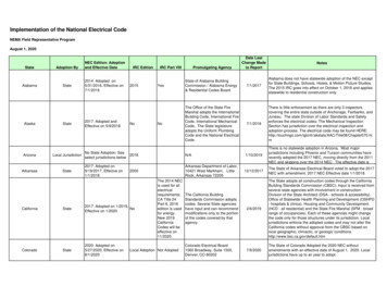
Transcription
HI-8456, HI-8457, HI-8458Octal ARINC 429 Line Receivers withIntegrated DO-160G Level 3 Lightning ProtectionApril 2020GENERAL DESCRIPTIONFEATURESHolt’s family of octal ARINC 429 line receivers, HI-8456,HI-8457 and HI-8458 include internal lightning protectioncircuitry which ensures compliance with RTCA/DO160G, Section 22 Level 3 Pin Injection Test WaveformSet A (3 & 4), Set B (3 & 5A) and Set Z (3 & 5B) withoutthe use of any external components. Each devicecontains 8 independent ARINC 429 line receivers. Pinsurge levels for Level 3 are summarized V/300AThe devices are designed to operate from either a 5V or3.3V supply in a high noise environment, with an inputcommon mode voltage range of 30V. Each receiverchannel translates incoming ARINC 429 data bussignals to a pair of TTL / CMOS outputs.In the case of HI-8456 and HI-8458, the TESTA andTESTB inputs bypass the analog inputs for testingpurposes. They force the outputs of all eight receiversto the specified ZERO, ONE or NULL state. The ARINCinputs are ignored when the devices are in test mode.The HI-8456 has a single test port which controlsall 8 channels simultaneously. The HI-8458 has twoindependent test ports, each controlling a bank of 4channels. Test inputs are not implemented on HI-8457and are internally connected to logic 0. The truth tablefor the TESTA and TESTB inputs is shown in Table 1.The HI-8456 and HI-8457 are exact drop in replacementsfor DEI1046 and DEI1047 respectively. The HI-8458 ispin-to-pin compatible with Holt’s HI-8448 and is also adrop-in replacement for the DEI1148 (44-pin PQFP). Apart number cross reference is included in Table 2.ooThe parts are available in Industrial -40 C to 85 C, orooExtended, -55 C to 125 C temperature ranges. Optionalburn-in is available on the extended temperature range. Internal lightning protection circuitry ensurescompliance with RTCA/DO-160G, Section 22Level 3 Pin Injection Test Waveform Set A (3 &4), Set B (3 & 5A) and Set Z (3 & 5B) Direct connection to ARINC 429 bus with noexternal components High input common mode voltage range of 30V 3.3V or 5.0V single supply operation Test inputs bypass analog inputs and force digitaloutputs to a one, zero, or null state (not availableon HI-8457) Industrial and Extended temperature ranges Burn-in availablePIN CONFIGURATION (TOP 34633IN5AIN5BIN6AIN6BIN7AIN7BIN8AIN8BNC* TESTA* UT6BOUT7AOUT7BOUT8AOUT8B38 Pin Plastic TSSOP Package* No Connect on HI-8457DS8458 Rev. FDownloaded from Arrow.com.HOLT INTEGRATED CIRCUITSwww.holtic.com104/20
HI-8456, HI-8457, HI-8458Table 1. Function TableARINCINPUTSINA - INBTESTA(1)TESTB(1)OUTAOUTB-2.5 to 2.5V0000 -6.5V0001 6.5V0010x0101x1010x1100Note (1): Not available on HI-8457.FUNCTIONAL DESCRIPTIONFigure 1 shows the general architecture of an ARINC 429 receiver. The receiver operates off the VDD supply only. Theinputs INA and INB may be connected directly to the ARINC 429 bus. Internal lightning protection circuitry ensurescompliance with RTCA/DO-160G, Section 22 Level 3 Pin Injection Test Waveform Set A (3 & 4), Set B (3 & 5A) andSet Z (3 & 5B) without the use of any external components.After level translation, the inputs are buffered and become inputs to a differential amplifier. The amplitude of thedifferential signal is compared to levels derived from a divider between VDD and Ground. The nominal settingscorrespond to a One/Zero amplitude of 6.0V and a Null amplitude of 3.3V.The status of the ARINC receiver input is latched. A Null input resets the latches and a One or Zero input sets thelatches.The logic at the output is controlled by the test signal which is generated by the logical OR of the TESTA and TESTBpins (not available on HI-8457). If TESTA and TESTB are both One, the outputs are pulled low. This allows the digitaloutputs of a transmitter to be connected to the test inputs through control logic for system self-test purposes.HOLT INTEGRATED CIRCUITS2Downloaded from Arrow.com.
HI-8456, HI-8457, HI-8458BLOCK HTESTARTESTBNULLFigure 1. Line Receiver Block BTESTAATESTABTESTATESTBTESTBATESTBB(Test inputs notconnected on 8BHI-8458HI-8456 / HI-8457Figure 2. Block Diagrams.HOLT INTEGRATED CIRCUITS3Downloaded from Arrow.com.
HI-8456, HI-8457, HI-8458Table 2. Cross Reference TableDEIPart NumberHoltPart NumberPackageTest in TSSOPYes 55 / 85oCDEI1046-TMS-GHI-8456PSTF38-pin TSSOPYes 55 / 125oCDEI1047-TES-GHI-8457PSTF38-pin TSSOPNo 55 / 85oCDEI1047-TMS-GHI-8457PSTF38-pin TSSOPNo 55 / 125oCDEI1148-QES-GHI-8458PQTF44-pin PQFPYes 55 / 85oCDEI1148-QMS-GHI-8458PQTF44-pin PQFPYes 55 / 125oCHOLT INTEGRATED CIRCUITS4Downloaded from Arrow.com.
HI-8456, HI-8457, HI-8458PIN DESCRIPTIONSTable 3. HI-8458 Pin DescriptionsSymbolFunctionDescriptionIN[8:1]AARINC INPUTReceiver [8:1] positive inputIN[8:1]BARINC INPUTReceiver [8:1] negative inputTESTAALOGIC INPUTPositive test input A for odd channelsTESTABLOGIC INPUTNegative test input A for odd channelsTESTBALOGIC INPUTPositive test input B for even channelsTESTBBLOGIC INPUTNegative test input B for even channelsOUT[8:1]BLOGIC OUTPUTReceiver [8:1] “ZERO” outputOUT[8:1]ALOGIC OUTPUTReceiver [8:1] “ONE” outputGNDPOWERGround supply voltageVDDPOWER 3.3V or 5V supply voltageNCNo ConnectNo connectTable 4. HI-8456/HI-8457 Pin DescriptionsSymbolFunctionDescriptionIN[8:1]AARINC INPUTReceiver [8:1] positive inputIN[8:1]BARINC INPUTReceiver [8:1] negative inputTESTALOGIC INPUTPositive test input (not available on HI-8457)TESTBLOGIC INPUTNegative test input (not available on HI-8457)OUT[8:1]BLOGIC OUTPUTReceiver [8:1] “ZERO” outputOUT[8:1]ALOGIC OUTPUTReceiver [8:1] “ONE” outputGNDPOWERGround supply voltageVDDPOWER 3.3V or 5V supply voltageNCNo ConnectNo connectHOLT INTEGRATED CIRCUITS5Downloaded from Arrow.com.
HI-8456, HI-8457, HI-8458ABSOLUTE MAXIMUM RATINGSSupply Voltage (VDD)-0.3V to 7VLogic input voltage rangeARINC input voltage-0.3V to 5.5VDC-120V to 120VAC120Vrms @ 400HzSolder Temperature (reflow)Storage Temperatureoo260 Co-65 C to 150 CESD-HBM (JS-001-2012)Logic and supply pins2,000VARINC 429 bus input pins1,000VRTCA/DO-160G, Section 22 pin 500A5B700V/500ARECOMMENDED OPERATING CONDITIONSSupply VoltagesVDD . 3.0V to 5.5VTemperature RangeooIndustrial Screening . -40 C to 85 CooExtended Temp Screening . -55 C to 125 CNOTE: Stresses above absolute maximum ratings or outside recommended operating conditions may cause permanent damage to the device.These are stress ratings only. Operation at the limits is not recommended.HOLT INTEGRATED CIRCUITS6Downloaded from Arrow.com.
HI-8456, HI-8457, HI-8458ELECTRICAL CHARACTERISTICSTable 5. DC Electrical CharacteristicsVDD 5.0V 10% or 3.3V 10%, GND 0V, TA Operating Temperature Range (unless otherwise stated)ParametersSymbolTest ConditionsMinTypMaxUnitsONE or ZEROVDINDifferential Input voltage6.51013VNULLVNINDifferential Input voltage2.5VCommon modeVCOMWith respect to GND 30 30VINA to INBRDIFFSupplies floating280kΩInput to GND or VDDRSUPSupplies floating140kΩARINC INPUTSInput VoltageInput ResistanceInput HysteresisInput CapacitanceVHYS0.51.0VARINC differentialCADARINC single endedto GNDCASHighVIHLowVILSinkIIHVIH VDDSourceIILVIL 0V-1.0μAHighVOHCIOH -100μAVDD 0.2VLowVOLCIOL 100μAGND 0.2VIDDHigh-speed.100% duty cycle.CL 15pF. VDD 5.5V.18mA510pF10pFTEST INPUTSLogic Input VoltageLogic Input Current2.0V0.8V200μAOUTPUTSLogic Output Voltage(CMOS)SUPPLY CURRENTVDD CurrentHOLT INTEGRATED CIRCUITS7Downloaded from Arrow.com.
HI-8456, HI-8457, HI-8458Table 6. AC Electrical CharacteristicsVDD 5.0V 10% or 3.3V 10%, GND 0V, TA Operating Temperature Range (unless otherwise stated)ParametersSymbolTest ConditionstLHMinTypMaxUnitsCL 50pF150300nstHLCL 50pF150300nsOutput Rise TimetR10% to 90%1550nsOutput Fall TimetF90% to 10%1550nsSWITCHING CHARACTERISTICSPropagation DelayPropagation DelayIN to OUTTEST to OUTtTOH50nstTOL50nsHOLT INTEGRATED CIRCUITS8Downloaded from Arrow.com.
HI-8456, HI-8457, HI-8458LIGHTNING INDUCED TRANSIENT VOLTAGE WAVEFORMSWaveform 3.V or ILargestPeak25% to 75%of Largest Peak50%0tFigure 3. DO-160G Lightning Induced Transient Voltage Waveform 3.Voc 600V, Isc 24A, Frequency 1MHz 20%.Waveform 4.V or IPeakT1 6.4µs 20%T2 70µs 20%50%0T1T2tFigure 4. DO-160G Lightning Induced Transient Voltage Waveform 4.Voc 300V, Isc 60A.HOLT INTEGRATED CIRCUITS9Downloaded from Arrow.com.
HI-8456, HI-8457, HI-8458Waveform 5.V or IPeak5A: T1 40µs 20%T2 120µs 20%5B: T1 50µs 20%T2 500µs 20%50%0T1T2tFigure 5. DO-160G Lightning Induced Transient Voltage Waveforms 5A and 5B.Voc 300V, Isc 300A.HOLT INTEGRATED CIRCUITS10Downloaded from Arrow.com.
HI-8456, HI-8457, HI-8458ADDITIONAL PACKAGE AND PIN T6BOUT7AOUT7BOUT8AOUT8BIN8B44 43 42 41 40 39 38 37 36 35 34 -IN3AIN2BIN2AIN1BIN1ANCOUT1AOUT1BOUT2AOUT2BOUT3A38 Pin Plastic TSSOP PackageHI-8458PQOctalReceiver33 32 31 30 29 28 27 26 25 24 23 -OUT3BOUT4AOUT4BNCVDDNCVSSNCOUT5AOUT5BOUT6AIN6B IN7A IN7B IN8A IN8B NC OUT8B OUT8A OUT7B OUT7A OUT6B -1213141516171819202122IN3B - 1IN4A - 2IN4B - 3NC - 4TESTAA - 5TESTAB - 6TESTBA - 7TESTBB - 8IN5A - 9IN5B -10IN6A - 1144-Pin Plastic Quad Flat Pack (PQFP)HOLT INTEGRATED CIRCUITS11Downloaded from Arrow.com.
44 43 42 41 40 39 38 37 36 35 34 -8456, HI-8457, HI-8458HI-8458PCOctalReceiver33 32 31 30 29 28 27 26 25 24 23 -IN6B IN7A IN7B IN8A IN8B NC OUT8B OUT8A OUT7B OUT7A OUT6B -1213141516171819202122IN3B - 1IN4A - 2IN4B - 3NC - 4TESTAA - 5TESTAB - 6TESTBA - 7TESTBB - 8IN5A - 9IN5B -10IN6A - 1144-Pin Plastic QFNHOLT INTEGRATED CIRCUITS12Downloaded from 6A
HI-8456, HI-8457, HI-8458ORDERING INFORMATIONHI - 845xxx x x (Plastic)PART NUMBERBlankFPART NUMBERLEAD FINISHTin / Lead (Sn / Pb) Solder100% Matte Tin (Pb-free, RoHS compliant)TEMPERATURE RANGEoFLOWBURN INoI-40 C to 85 CINoT-55oC to 125oCTNoMYesMPART NUMBERoo-55 C to 125 CPACKAGE DESCRIPTIONTEST PINS8456PS38 PIN PLASTIC TSSOP (38HS)Y8457PS38 PIN PLASTIC TSSOP (38HS)N8458PS38 PIN PLASTIC TSSOP (38HS)Y8458PQ44 PIN PLASTIC QUAD FLAT PACK (44PMQS)YHI - 8458PC x x (Plastic)PART NUMBERBlankFPART NUMBERILEAD FINISHNiPdAuNiPdAu (Pb-free, RoHS compliant)TEMPERATURE RANGE-40oC to 85oCooFLOWBURN ININoT-55 C to 125 CTNoM-55oC to 125oCMYesPART NUMBER8458PCPACKAGE DESCRIPTION44 PIN PLASTIC QFN (44PCS)HOLT INTEGRATED CIRCUITS13Downloaded from Arrow.com.TEST PINSY
HI-8456, HI-8457, HI-8458REVISION HISTORYRevisionDS8458,DateDescription of ChangeRev. New.01/27/16Initial ReleaseRev. A04/01/16Correct typos on 44-pin PQFP and QFN packages (Pin 26 listed twice).Rev. B08/11/16Remove Logic Output Voltage spec. (VOH, VOL). Use CMOS spec. (VOHC, VOLC).Rev. C12/05/16Remove Power Dissipation spec from “Absolute Maximum Ratings”. UpdateSupply Current spec in “Electrical Characteristics”.Rev. D06/28/17Update lightning waveforms Voc value in “Absolute Maximum Ratings” table.Rev. E09/20/17Update Functional Description.Rev. F04/28/2020Add ARINC AC Input Voltage to Absolute Maximum Ratings table.Update QFN lead finish to NiPdAu.HOLT INTEGRATED CIRCUITS14Downloaded from Arrow.com.
HI-8456, HI-8457, HI-8458PACKAGE DIMENSIONS38-PIN PLASTIC TSSOPmillimeters (inches)Package Type: 38HS9.700 0.100(0.382 0.004)6.400 0.150(0.252 0.006)0.145 0.055(0.006 0.002)4.400 0.100(0.173 0.004)Pin 1See Detail A0.220 0.050(0.0087 0.002)0.925 0.125(0.036 0.005)0.500BSC(0.0197))0 to 8 0.100 0.050(0.004 0.002)0.600 0.150(0.024 0.006)BSC “Basic Spacing between Centers”is theoretical true position dimension andhas no tolerance. (JEDEC Standard 95)44-PIN PLASTIC QUAD FLAT PACK (PQFP)Detail Amillimeters (inches)Package Type: 44PMQS0.230 MAX.(0.009)0.80BSC(0.031)10.000 BSC(0.394)SQ.13.200 BSC(0.520)SQ.0.370 0.080(0.015 0.003)0.880 0.150(0.035 0.006)1.60typ(0.063)0.20min(0.008)See Detail A2.70MAX.(0.106)2.00 0.20(0.079 0.008)0.13R MIN. Detail A(0.005)BSC “Basic Spacing between Centers”is theoretical true position dimension andhas no tolerance. (JEDEC Standard 95)HOLT INTEGRATED CIRCUITS15Downloaded from Arrow.com.0.30R MAX.(0.012)0 Θ 7
HI-8456, HI-8457, HI-845844-PIN PLASTIC CHIP-SCALE PACKAGE (QFN)millimeters (inches)Package Type: 44PCS7.00BSC(0.276)5.50 0.050(0.217 0.002)0.50 BSC(0.0197)7.00BSC(0.276)5.50 0.050(0.217 0.002)Top View1.00max(0.039)0.200 typ(0.008)BSC “Basic Spacing between Centers”is theoretical true position dimension andhas no tolerance. (JEDEC Standard 95)Electrically isolated heat sinkpad on bottom of package.Connect to any ground orpower plane for optimumthermal dissipation.HOLT INTEGRATED CIRCUITS16Downloaded from Arrow.com.BottomView0.25 0.050(0.010 0.002)0.400 0.050(0.016 0.002)
circuitry which ensures compliance with RTCA/DO-160G, Section 22 Level 3 Pin Injection Test Waveform Set A (3 & 4), Set B (3 & 5A) and Set Z (3 & 5B) without the use of any external components. Each device contains 8 independent ARINC 429 line receivers. Pin surge levels for Level 3 are summarized below. Waveform 3 Waveform 4 Waveform 5A .