Transcription
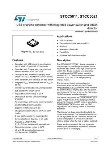
DATA SHEETwww.onsemi.comIntegrated Load SwitchFDC6330LTSOT 23 6CASE 419BLDescriptionMARKING DIAGRAMThis device is particularly suited for compact power managementin portable electronic equipment where 3 V to 20 V input and 2.3 Aoutput current capability are needed. This load switch integratesa small N Channel power MOSFET (Q1) which drives a largeP Channel power MOSFET (Q2) in one tiny SUPERSOTt 6package.Features VDROP 0.20 V @ VIN 12 V, IL 2.5 A, R(on) 0.08 W VDROP 0.20 V @ VIN 5 V, IL 1.6 A, R(on) 0.125 W Control MOSFET (Q1) Includes Zener Protection for ESD Ruggedness ( 6 kV Human Body Model)High Performance POWERTRENCH Technology for ExtremelyLow On ResistanceSUPERSOT 6 Package Design Using Copper Lead Frame forSuperior Thermal and Electrical CapabilitiesThis is a Pb Free and Halide Free DeviceApplication Power Management Load ActuationVIN,R14ON/OFF53VOUT, C12VOUT, C11R2&E&Y&.330&G&E&Y&.330&G Designates Space Binary Calendar Year Coding Scheme Pin One Dot Specific Device Code Date CodeORDERING INFORMATIONDeviceFDC6330LPackageShipping†TSOT 23 6(Pb Free)3000 /Tape & Reel†For information on tape and reel specifications,including part orientation and tape sizes, pleaserefer to our Tape and Reel Packaging SpecificationBrochure, BRD8011/D.Q2Q1R1, C16See Application Circuit (Figure 2)Figure 1.VDROP IN OUTON/OFFFigure 2. Equivalent Circuit Semiconductor Components Industries, LLC, 1999December, 2021 Rev. 3Downloaded from Arrow.com.1Publication Order Number:FDC6330L/D
FDC6330LABSOLUTE MAXIMUM RATINGS TA 25 C unless otherwise notedSymbolVINVON/OFFIDPDTJ, TSTGESDValueUnitInput Voltage Range (Note 1)Parameter3 20VOn/Off Voltage Range1.5 8VLoad Current Continuous (Note 2)2.3ALoad Current Pulsed10Maximum Power Dissipation (Note 1)Operating and Storage Temperature Range0.7W 55 to 150 C6kVElectrostatic Discharge Rating MIL STD 883D Human Body Model (100 pF / 1500 W)Stresses exceeding those listed in the Maximum Ratings table may damage the device. If any of these limits are exceeded, device functionalityshould not be assumed, damage may occur and reliability may be affected.THERMAL CHARACTERISTICS TA 25 C unless otherwise notedSymbolParameterValueUnitRqJAThermal Resistance, Junction to Ambient (Note 2)180 C/WRqJCThermal Resistance, Junction to Case (Note 2)60 C/WELECTRICAL CHARACTERISTICS TA 25 C unless otherwise notedSymbolParameterTest ConditionsMinTypMaxUnitVIN 20 V, VON/OFF 0 V 1mA 0.2VOFF CHARACTERISTICSIFLLeakage CurrentON CHARACTERISTICS (Note 3)VDROPConduction VoltageVIN 12 V, VON/OFF 3.3 V, IL 2.5 AVIN 5 V, VON/OFF 3.3 V, IL 1.6 A 0.2RDS(on)Q2 Static On ResistanceVGS 12 V, ID 2.3 A 0.0540.08VGS 5 V, ID 1.9 A 0.0810.125VDROP 0.2 V, VIN 12 V, VON/OFF 3.3 V2.5 VDROP 0.2 V, VIN 5 V, VON/OFF 3.3 V1.6 ILLoad CurrentWAProduct parametric performance is indicated in the Electrical Characteristics for the listed test conditions, unless otherwise noted. Productperformance may not be indicated by the Electrical Characteristics if operated under different conditions.NOTES:1. Range of Vin can be up to 30 V, but R1 and R2 must be scaled such that VGS of Q2 does not exceed 20 V.2. RqJA is the sum of the junction to case and case to ambient thermal resistance where the case thermal reference is defined as the soldermounting surface of the drain pins. RqJC is guaranteed by design while RqJA is determined by the user’s board design.3. Pulse Test: Pulse Width 300 ms, Duty Cycle 2.0%.Q2INOUTC1R1CiON/OFFQ1CoLoadR2External Component Recommendation:For applications where Co 1 mF.For slew rate control, select R2 in the range of 1k 4.7 kW.For additional in rush current control, C1 1000 pF can beadded.Select R1 so that the R1/R2 ratio ranges from 10 100.R1 is required to turn Q2 off.Figure 3. FDC6330L Load Switch Applicationwww.onsemi.com2Downloaded from Arrow.com.
FDC6330LTYPICAL CHARACTERISTICS0.40.5TJ 125 C0.2TJ 25 C0.1VIN 12 VVON/OFF 1.5 8 VPW 300 ms, D 2%01230.30.2VIN 50 VVON/OFF 1.5 8 VPW 300 ms, D 2%0.1054TJ 25 C012354IL (A)IL (A)Figure 4. Conduction Voltage DropVariation with Load CurrentFigure 5. Conduction Voltage Drop Variationwith Load Current0.25IL 1 AVON/OFF 1.5 8 VPW 300 ms, D 2%0.2RON (W)VDROP (V)VDROP (V)0.30TJ 125 C0.40.15TJ 125 C0.1TJ 25 C0.05024681012VIN (V)Figure 6. On Resistance Variation with Input Voltage1r(t), Normalized EffectiveTransient Thermal ResistanceD 0.50.50.2RqJA (t) r(t) * RqJARqJA See Note ingle Pulse0.001TJ TA P * RqJA (t)Duty Cycle, D t1/t20.010.1t1, Time (s)110100300Figure 7. Transient Thermal Response CurveNOTE:Thermal characterization performed on the conditions described in Note 2.Transient thermal response will change depending on the circuit board design.SUPERSOT is a trademark and POWERTRENCH is a registered trademark of Semiconductor Components Industries, LLC dba “onsemi”or its affiliates and/or subsidiaries in the United States and/or other countries.www.onsemi.com3Downloaded from Arrow.com.
MECHANICAL CASE OUTLINEPACKAGE DIMENSIONSTSOT23 6 LeadCASE 419BLISSUE A1SCALE 2:1DATE 31 AUG 2020GENERICMARKING DIAGRAM*XXX MGG1XXX Specific Device CodeM Date CodeG Pb Free Package(Note: Microdot may be in either location)*This information is generic. Please refer todevice data sheet for actual part marking.Pb Free indicator, “G” or microdot “ G”,may or may not be present. Some productsmay not follow the Generic Marking.DOCUMENT NUMBER:DESCRIPTION:98AON83292GTSOT23 6 LeadElectronic versions are uncontrolled except when accessed directly from the Document Repository.Printed versions are uncontrolled except when stamped “CONTROLLED COPY” in red.PAGE 1 OF 1ON Semiconductor andare trademarks of Semiconductor Components Industries, LLC dba ON Semiconductor or its subsidiaries in the United States and/or other countries.ON Semiconductor reserves the right to make changes without further notice to any products herein. ON Semiconductor makes no warranty, representation or guarantee regardingthe suitability of its products for any particular purpose, nor does ON Semiconductor assume any liability arising out of the application or use of any product or circuit, and specificallydisclaims any and all liability, including without limitation special, consequential or incidental damages. ON Semiconductor does not convey any license under its patent rights nor therights of others. Semiconductor Components Industries, LLC, 2018Downloaded from Arrow.com.www.onsemi.com
onsemi,, and other names, marks, and brands are registered and/or common law trademarks of Semiconductor Components Industries, LLC dba “onsemi” or its affiliatesand/or subsidiaries in the United States and/or other countries. onsemi owns the rights to a number of patents, trademarks, copyrights, trade secrets, and other intellectual property.A listing of onsemi’s product/patent coverage may be accessed at www.onsemi.com/site/pdf/Patent Marking.pdf. onsemi reserves the right to make changes at any time to anyproducts or information herein, without notice. The information herein is provided “as is” and onsemi makes no warranty, representation or guarantee regarding the accuracy of theinformation, product features, availability, functionality, or suitability of its products for any particular purpose, nor does onsemi assume any liability arising out of the application or useof any product or circuit, and specifically disclaims any and all liability, including without limitation special, consequential or incidental damages. Buyer is responsible for its productsand applications using onsemi products, including compliance with all laws, regulations and safety requirements or standards, regardless of any support or applications informationprovided by onsemi. “Typical” parameters which may be provided in onsemi data sheets and/or specifications can and do vary in different applications and actual performance mayvary over time. All operating parameters, including “Typicals” must be validated for each customer application by customer’s technical experts. onsemi does not convey any licenseunder any of its intellectual property rights nor the rights of others. onsemi products are not designed, intended, or authorized for use as a critical component in life support systemsor any FDA Class 3 medical devices or medical devices with a same or similar classification in a foreign jurisdiction or any devices intended for implantation in the human body. ShouldBuyer purchase or use onsemi products for any such unintended or unauthorized application, Buyer shall indemnify and hold onsemi and its officers, employees, subsidiaries, affiliates,and distributors harmless against all claims, costs, damages, and expenses, and reasonable attorney fees arising out of, directly or indirectly, any claim of personal injury or deathassociated with such unintended or unauthorized use, even if such claim alleges that onsemi was negligent regarding the design or manufacture of the part. onsemi is an EqualOpportunity/Affirmative Action Employer. This literature is subject to all applicable copyright laws and is not for resale in any manner.PUBLICATION ORDERING INFORMATIONLITERATURE FULFILLMENT:Email Requests to: orderlit@onsemi.comonsemi Website: www.onsemi.com Downloaded from Arrow.com.TECHNICAL SUPPORTNorth American Technical Support:Voice Mail: 1 800 282 9855 Toll Free USA/CanadaPhone: 011 421 33 790 2910Europe, Middle East and Africa Technical Support:Phone: 00421 33 790 2910For additional information, please contact your local Sales Representative
DATA SHEET www. onsemi.com Semiconductor Components Industries, LLC, 1999 December, 2021 ï Rev. 3 1 Publication Order Number: FDC6330L/D Integrated Load Switch FDC6330L Description This device is particularly suited for compact power management in portable electronic equipment where 3 V to 20 V input and 2.3 A output current capability are needed.