Transcription
Reliable Low-Power Design in the Presence of DeepSubmicron NoiseNaresh ShanbhagK. SoumyanathCoordinated Science LabECE DepartmentUniversity of Illinois atUrbana-ChampaignUrbana, IL-61801.Circuits Research LabIntel CorporationHillsboro, OR.ABSTRACTSamuel MartinBell LabsLucent Technologies, MurrayHill, NJ.with large signal powers was a common means of achieving reliable communication of information. A key impactof [27], relevant to the discussion here, was to enable modern day communication systems to achieve a high degree ofreliability with signal levels that are comparable to noise inmany cases thereby achieving the dual goals of reliability andenergy-efficiency. Interestingly, Winograd in 1963 providedthe following motivation for his work in [32]: "As computersbecome larger, faster, and more complex, it seems unlikely,despite recent developments in microelectronics, that component reliability will become sufficiently good to permitthe immediate synthesis of complex computing organs fromcomponents that for all practical purposes may be considered infallible."Scaling of feature sizes in semiconductor technology has beenresponsible for increasingly higher computational capacity ofsilicon. This has been the driver for the revolution in communications and computing. However, questions regardingthe limits of scaling (and hence Moore's Law) have arisen inrecent years due to the emergence of deep submicron noise.The tutorial describes noise in deep submicron CMOS andtheir impact on digital as well as analog circuits. In particular, noise-tolerance is proposed as an effective means forachieving energy and performance efficiency in the presenceof DSM noise.1. INTRODUCTIONSince, late eighties, enormous advances have been made inWinograd's prediction was much ahead of its time. Semideveloping tools and techniques that enable the design ofconductor process technology, the design tools, techniquesenergy-efficient ICs. These include techniques at variousand methodologies have made integrated circuits a reliablelevels of the design abstraction. Relentless scaling of featuremedium for implementation of information processors unsizes in semiconductor technology [14] following Moore's Lawtil now. DSM noise along with increasing complexity ofhas rendered the ability to significantly improve performancesystems-on-a-chip (SOC) solutions, and increasingly strinand lower power of integrated circuits at an affordable cost.gent requirements on speed and power have made the deThis has been the driver for the revolution in the computingsign of reliable and eficient (an terms of energy and/or perand communication infrastructure. However, with featureformance) SOC a problem of great significance: one thatsizes being reduced towards 0.1 - 0.05pm generations, queshas a direct bearing on the future of Moore's Law. Solvtions have arisen regarding the ability to achieve favorableing this problem requires a new design paradigm that adcost vs. performance/power trade-offs in future CMOS techdresses the reliability of the system as opposed to that ofnologies. The emergence of deep submicron (DSM) noisethe component (devices, and circuits) even though the cause[28] in the form of cross-talk, leakage, supply noise, as well as(DSM noise) of unreliable system behavior is in the compoprocess variations is making it increasingly hard to achievenent. Such a paradigm will be inherently multidisciplinarythe desired level of noise-immunitv while maintaining theas it may bring in information-theory for computing boundshistoric improvement trends in performance and energy-efficiency.on energy-efficiencyand reliability, error-control coding andIis well-positioned to address the problem of reliable lowpower design. The fault-tolerant and low-power design.communities have independently addressed the reliability andthe energy-efficiency issues, respectively. However, joint optimization of these two metrics is essential to ensure thatbenefits of large scale integration can be continually reaped.Permission to make digital or hard copies of all or part of this work forpersonal or classroom use is granted without fee provided that copiesare not made or distributed for profit or commercial advantage and thatcopies bear this notice and the full citation on the first page. To copyotherwise, or republish, to post on servers or to redistribute to lists,requires prior specific permission and/or a fee.ISLPED '00,Rapallo, Italy.Copyright 2000 ACM 1-581 13-190-9/00/0007. 5.00.In addition to discussing trends in DSM noise sources, andtheir influence on high-performance and low-power design295
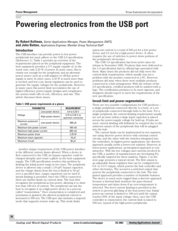
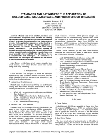
Noisv Vu10-In-30.40.60.81Time (Normalized)-lXLkgut-OXLkgLkgi . 2Figure 2: Noise scaling trend at the dynamic nodeof a domino circuit.Figure 1: Impact of power supply bounce on a dynamic D-latch: (a) transistor schematic, and (b) input and output waveform.Itechniques, this tutorial paper will present concrete approachesfor computing bounds on energy-efficiency in the presence ofDSM noise, and new circuit as well as algorithmic techniquesfor exploring the energy-efficiency vs. reliability curve. Keyconcepts will be emphasized through theoretical as well asmeasured results obtained in the VLSI Information Processing Systems (ViPS) Research Group at University of Illinoisa t Urbana-Champaign, the Circuits Research Laboratory(CRL) a t Intel Corp., Portland, Oregon and Bell Laboratories at Lucent Technologies, Murray Hill, New Jersey.I\VoutvddThe paper is organized as follows. In section 2, we describeDSM noise sources and their trends with scaling, noise metrics and their measurement. In section 3, we desribe aninformation-theoretic framework for computing achievablebounds on energy-efficiency in the presence of DSM noise.A key conclusion of this section will be that noise-tolerance isnecessary to approach the energy-efficiency bounds. Circuitas well as algorithmic techniques for noise-tolerance will beillustrated in section 4. The role of noise in analog circuitswill be discussed in section 5.32J,--7Figure 3: Dynamic noise-immunity metrics: (a)noise-immunity curves (NICs), (b), input and (c)output waveforms employed in defining unity noisegain ( U N G ) and (d) the "noise wall" in the delay vs.U N G plot.NOISE IN DEEP SUBMICRON CMOS2.1 DSM Noise Mechanisms2.Noise in DSM circuits is defined as any disturbance thatdrives node voltages and/or currents away from a nominalvalue causing permanent as well as intermittent logic failure. Increased delay as well as accidental discharge/chargeof dynamic nodes are common mechanisms for such failures.Figure 1 illustrates one such error. When D Vdd,if an inthenductive kick raises the supply node above Vddthe topmost PMOS at the input in Fig. l(a) will turn onresulting in a logic error as shown in Fig. l(b).a PMOS keeper. The data shows that this circuit techniqueis unsustainable when the leakage is set a t 9X (e.g O.1pm)of the base technology (e.g 0.18pm). 2.2 Noise-Immunity MetricsA commonly employed definition of noise-immunity [15] arethe static noise margins N M L VZL- VOL and N M H VOH- VZH,where VOL,and VO/OHare the minimum andmaximum output voltage levels, respectively, and VZLandVIH are the low and high input voltage levels a t which theDC voltage transfer curve of a gate has a gain of -1. Staticnoise margins are conservative noise-immunity metrics because they do not account for the fact that digital gates areinherently low-pass in nature and thus can filter out noisepulses with amplitude V, that are greater than N M L orN M H provided the noise pulse width Tn is sufficiently narrow, i.e., the noise pulse has predominantly high frequencycomponents.Noise sources that have substantial impact on the performance of digital circuits include ground bounce, IR drop,crosstalk, charge sharing, process variations, charge leakage, alpha particles, electro-magnetic radiation, etc., [17,281. These problems worsen as technology scales furtherand hence are referred to as deep submicron (DSM) noise.For example, a key feature of the scaling trend is the increasein I o f f (by 3X) with every successive technology generation.Fig. 2 shows the impact of this trend on the dynamic node ofa fully loaded (fanout 9) 8-wide NOR domino circuit with296
Lab has shown that for wide OR gates, a 11- 14% improvement in speed results in a 40 - 50% degradation in U N Gmetric for a O.lpm technology.Hence, dynamic noise-immunity metrics such as the noiseimmunity curve (NIC) [16] in Fig. 3(a) are required. TheVn)for whichNIC of a digital gate is a locus of points (Tn,the gate just makes a logic error (defined as the event whenthe output crosses a predefined voltage threshold). The NICof a digital gate provides the following information:Given the well-known relationship between delay and energy, it is clear that designers need to explicitly consider thetrade-off between power, performance and noise-immunityin a unified manner. Noise analysis tools and techniquessuch as [ I ] that inform the designer of the noise characteristics will be much needed. The noise wall in Fig. 3(d), reminiscent of the power wall being faced by designers of highperformance systems, can be breached only by a new designparadigm that is aware of bounds on achievable energyefficiency and strives to achieve system reliability (as opposed to component reliability) through a combination ofcircuit, algorithmic and technology-based solutions. In thenext section, we present an information-theoretic frameworkfor computing achievable bounds on energy-efficiency in thepresence of DSM noise.1. all points on and above the NIC represents error causing noise pulses while all noise pulses below the NICdo not cause any errors. Hence, higher the NIC of agate, the less susceptible is the gate to noise.2. the vertical asymptote of the curve provides the bestcase delay of the circuit, in general. For single-inputgates such as the inverter, this asymptote provides alsothe worst-case delay (or just the delay) of the circuit.Thus, noise-immunity and throughput are intimately(and inversely) related.The average noise threshold energy ( A N T E ) [31] is a convenient measure derived from a NIC that can be employedto compare the various circuit techniques and is defined asA N T E f E (Vn2Tn),3. BOUNDS ON ENERGY-EFFICIENCYBeing able to compute achievable bounds on energy-efficiencyunder the constraint of reliable system operation provides adirect answer to question of how long can Moore's Law continue and motivates the designer to explore techniques forclosing the gap between efficiency of present day systemsand the bounds. Lower bounds on energy dissipation havebeen addressed by researchers in the integrated circuits area[20, 291. These bounds are derived under the constraint ofcomponent reliability. Information theoretic research [9, 22,321 has derived bounds on component reliability for achieving an arbitrary level of system reliability. The informationtheoretic approach satisfies the need to focus on system reliability as opposed to component reliability. However, whatis lacking in the latter approach is: ( 1 ) the missing link tophysical properties of semiconductor technology that permits the derivation of bounds on energy-efficiency and ( 2 )the inherent assumption of unbounded complexity for optimal systems. In this section, we present our recent work [ l o ,25, 261 that addresses the first issue while the second issueis addressed in section 4.(1)where E( ) denotes the average. As circuits are designed fora specific worst-case delay, the average in (1) is taken fornoise pulse widths ranging from the best case to the worstcase delay of the circuit. Usually noise-immunity enhancingtechniques incur power/performance penalty at the circuitlevel. Thus, normalizing A N T E ( N A N T E ) with the energyof the gate gives another metric that compares the effectiveness of different noise-tolerance techniques.Another measure of noise-immunity, referred to as the unitynoise gain ( U N G ) , can be obtained by injecting identicalnoise pulses into all inputs and measuring the resulting voltage output waveform VOutas shown in Fig. 3(b)-(c). Thenoise stimulus consists of a DC offset VDC (to account fori.e.,possible IR drops) and a scalable pulse Vpulse,Vnoise VDC Vpulse,(2)where the shape of Vpulseclosely mimics the real noise pulses.U N G is defined as the amplitude of input noise Vnoisethati.e.,causes an equal-amplitude output noise at Vout,U N G {Vnoise : Vnoise Vout} .3.1 Information-Theoretic FrameworkInformation theory takes a probabilistic model for signalsand noise. For example, an information bearing signal sourceis defined as one that generates symbols Y from the setdefSy YO,Y1,. .YL-I with a probability pi Pr(Y Yi)for i 0,. . . ,L - 1. The information content of such asignal is given by its entropy [27] H ( Y )as follows(3)Note that U N G is dependent on the noise pulse width Tnoise.An interesting interpretation of U N G can be obtained in theis small enough for small-signal analysis tocase when Vpulsehold. In that case, U N G equals the input amplitude forwhich the small-signal gain (with V& being the bias point)(4)at frequency l/Tnoiseis unity. Thus, U N G can be viewed asthe AC version of the static noise margins N M L and N M HA useful relation quantity is the entropy function h ( p ) de(Note: U N G L and U N G H can be similarly defined for staticfined as follows:circuits).h(P) - P b 2 ( P ) - (1- P ) k ? 2 ( 1 - P),The trade-off between performance and noise-immunity ismade explicit in Fig. 3(d), in which a unity slope line wouldrepresent a desirable scaling trend where the reduction innoise margin tracks delay (and Vdd)scaling. However, bothhigh and low V, technologies will fail to track this trend. Recent joint work between UIUC ViPS Group and Intel CRL(5)where 0 5 p 5 1. The inverse entropy function h-'(q) where0 5 h-l(q) 5 0.5 can similarly be defined.In [26], we have shown that any system function with inputX and output Y has a minimum information transfer rate297
subject to:where Po, 0.5tCLV&fc, Pstat and P,, are the capacitive,static and short-circuit components of power dissipation, t isthe transition activity, Eb is the energylbit of informationbeing transferred, km is the device transconductance andCL is the load capacitance. The term E is the probabilitythat a logic error occurs and is a function of the standarddeviation U N of the noise amplitude Vn thereby embodyingthe impact of DSM noise.Figure 4: The information-theoretic framework forDSM ICs: (a) framework components, and (b) implementation.There is an intricate relationship between R, U N , t, C L ,V d d ,Vt, f c , IC, and E in (9), (lo), and (11). By solving the aboveproblem in its most general form in [13],we have shown thatin a scenario where Pcapdominates, the supply voltagefor minimum energy & & o p t is greater than the minimum supply voltage ( V d d , m i n ) for reliable operation,i.e., minimum energy is consumed not when C R but whenC is close to R. Further, we have shown that for off-chipsignaling, the lower bounds on energy-efficiency are24X below the energy-efficiency achieved by present daysystems. For various special cases, we describe the followinginteresting results.requirement of R bits/s given bywhere H(Y) is the output entropy and fs is the rate a twhich X is being generated. The information transfer rateR is implementation-independent.The channel capacity per use C, [lo] is obtained by maximizing the mutual information I ( X ; Y) H ( Y ) - H(YIX)over all possible channel input distributions [27],C, max[H(Y) - H ( Y ( X ) ] .VP(X)The lower bound on fc for reliable operation of a symmetric,single output, noisy logic gate can be obtained from (10) as(7)Multiplying C, with the rate at which the channel is usedf c , we obtainc Cufc,The above equation indicates that as DSM noise (i.e., E)increases, the minimum frequency a t which the circuit needsto be clocked also increases.(8)where C is the information transfer capacity of the implementation. For DSM integrated circuits, fc, C,, and henceC are a complex function of the technology, circuit style andarchitecture. In particular, increases with V d d (because f cand noise margins increase) and decreases with DSM noise.The minimum vdue of V d d for reliable operation of a symmetric, single output, noisy logic gate, denoted by Vdd,,in,can be shown from (10-11) to satisfy the following quadratic,cIf the constraint C R is satisfied, then the joint sourcechannel coding theorem [27] guarantees that an encoderdecoder combination (see Fig. 4(b)) exists that guaranteesa vanishingly small probability of error at the decoder output. We refer to the constraint C R as the reliabilityconstraint. Thus, by making C approach R, we can obtaincircuit parameters values that that minimize energy of thenoisy implementation (not including the encoder-decoder)in Fig. 4(b) while maintaining reliability. For these boundsto be approachable in practice, one needs a low-complexity(low compared to the noisy circuit) encoder-decoder. In section 4, we show that a combination of circuit as well as algorithmic noise-tolerance techniques are excellent candidatesto employ for approaching the bounds.which clearly shows thatVdd,minincreases with DSM noise.The lower bound on transition activity a t the output of asymmetric, single output, noisy logic gate employing transition signaling can be obtained ast 1 h-l[; h ( 4 .Note, if fc fc,,in, V d d &,,inthen t 0.5 in (14).However, this condition may not result in minimum energydissipation. An increase in V d d leads to an increase in f cand hence a decrease in t. The decrease in t can offsetthe increase in V d d and f c resulting in a net reduction indynamic energy consumption. Hence, the rationale for thenon-intuitive result V d d , o p t V d d , m i n referred to earlier.3.2 Computing Lower BoundsBased upon the discussion so far, the following optimizationproblem can be formulated for a single output gate,In the absence of noise, i.e. E 0, substituting R Rfsbits/s and fc Rb fs (Rb is the number of code bits assignedper symbol) into (14), we obtain the lower bound on t forthe noiseless case [25].298
TTA,A2CLK{Figure 5: Lower bounds on energy dissipation forthe mirror technique.From the discussion so far it is clear that the lower boundsimprove (i.e., reduce) as the error frequency E reduces. Oneway to reduce E is to employ noise-tolerance circuit techniques [2, 4, 6, 311. These techniques add more circuit elements to the original domino gate and hence would incuran energy penalty at the same supply voltage. However, agood noise-tolerant circuit technique can achieve equal orbetter noise-immunity at a lower supply voltage than thecorresponding domino circuit. Thus, noise-tolerance techniques can improve the lower bounds on energy, providedthe reduction in E offsets the energy penalty due to noisetolerance. Recently, this conjecture was verified (see Fig. 5 )for a 3-input OR gate transferring information at a rateR 150Mbits/sec in 0.35pm CMOS [30]. This work indicates that the lower bound on energy consumption of thenoise-tolerant circuit is 31% below that of the conventionaldomino circuit. Further, this lower bound is achieved whenthe ANTE noise-immunity metric of the mirror techniqueis 1.64X more than that of the domino circuit technique.Further improvements in noise-immunity do not reduce thelower bounds because the energy penalty starts to dominate.(c)(4Figure 6: Noise-tolerant circuit techniques: (a) thePMOS pull-up, (b) the CMOS inverter, (c) the mirror, and (d) the twin-transistor techniques.4.1 Noise-tolerant Circuit DesignDynamic circuits, especially the wide-fanin OR gates using low & transistors for better pull-down speed, are errorprone due to their low switching threshold voltage V,t Vt. Increasing V,, improves noise-immunity at the expenseof power and/or performance. Nevertheless, we have already shown (see Fig. 5) that if the improvement in noiseimmunity (Le., reduction in E ) is sufficiently large comparedwith the energy penalty then the minimum energy consumedby the more complex noise-tolerant circuit will be smaller.Thus, noise-tolerant circuit techniques that effectively improve noise-immunity are required.The results in [30] were obtained for a noise voltage withstandard deviation of 400mV, which Fig. 5 indicates is comparable to V&,opt 1.1V. Similar results in [13, 261 pointclearly to noise-tolerance as a practical means of approaching the bounds on energy dissipation as described in thenext section.Several techniques have been developed so far to enhancethe noise-immunity of dynamic circuits. The first techniquereferred to as the PMOS pull-up technique [4] (see Fig. 6(a))utilizes a pull-up device to increase the source potential ofthe NMOS network thereby increasing the transistor threshold voltage & and V,t during the evaluate phase. This technique suffers from large static power dissipation. The CMOSinverter technique [2] utilizes a PMOS transistor for each input thereby adjusting V,t to equal that of a static circuit.This technique cannot be used for NOR-type circuits.4. NOISE-TOLERANTVLSIIn this section, we describe noise-tolerance techniques forcombating DSM noise while maintaining energy-efficiency.Motivation for noise-tolerance is derived from the informationtheoretic results of section 3 which indicate that signal andnoise powers need to be comparable in order to approachthe bounds on energy-efficiency. This means that from anenergy-efficiency perspective it is better to make errors andcorrect them rather than expending energy to reduce noise.The use of error-correcting codes for noisy gates [7,211 andarithmetic units [23, 241 have been considered before butnot in conjunction with energy-efficiency. Indeed, we willsee later that in order to satisfy the low-complexity constraint on the encoder-decoder combination in Fig. 4(b),noise-tolerance techniques at higher levels of the design abstraction such as the architectural and algorithmic levels arerequired. This is so that the energy cost of error control canbe amortized over complex blocks.The mirror technique [31] (see Fig. 6(c)) utilizes two identical NMOS evaluation networks and one additional NMOStransistor M I to pull up the source node of the upper NMOSnetwork to Vdd - & during the precharge phase therebyincreasing Vat.The mirror technique guarantees zero DCpower dissipation but a speed penalty is incurred if the transistors are not resized.The twin-transistor technique (see Fig. 6(d)) [ 5 , 61 utilizesan extra transistor for every transistor in the pull-down net299
Error ControlFigure 7: Measured noise-immunity curves for thetwin-transistor technique. .work in order to pull up the source potential. The twintransistor technique consumes no DC power. Both the mirror and twin transistor techniques have been experimentallyproved via the design and test of prototype chips in 0.35pmCMOS technology in the ViPS laboratory at UIUC. Figure 7 shows that the measured improvement in N I C for thetwin-transistor technique [6] is greater than 2.4X with a 15%increase in energy dissipation a t the same supply voltage.Soft Filler(c);:I.Soh Filter(4Fig1 .e 8: Algorithmic noise-tolerance (ANT) (a)and its use in soft DSP framework: (b) path delay distribution of a ripple-carry adder, (c) the prediction based error-control scheme, and (d) errorcancellation scheme.4.2 Algorithmic Noise-toleranceAlgorithmic techniques for handling intermittent errors incombination with noise-tolerant circuit techniques describedin the previous subsection, have the potential of approaching the lower bounds on energy envisaged by the configuration in Fig. 4(b). Research in fault-tolerant computing hasaddressed this problem to some extent, however the solutions do not address the energy-efficiency issue. Recently,we have proposed the notion of algorithmic noise-tolerance(ANT) [ll,121, whereby the statistical properties of signalsand the architecture are exploited to develop energy-efficienttechniques for mitigating soft errors at the algorithmic level.These techniques work best in the context of DSP and communication systems where the system performance metricsare in terms of S N R andfor bit error-rate ( B E R ) ,whichare statistical quantities themselves.critical path delay of the module. Figure 8(b) shows the pathdelay distribution of a ripple carry adder. Note that thereis one critical path that determines the value of Vdd,crit. Ifthe supply voltage is scaled beyond V&-crit (referred t o asvoltage overscaling (VOS)) then intermittent errors occur a tthe adder output whenever the inputs exciting the criticalpath appear. If the adder is in a filtering block then thisleads to a degradation in algorithmic performance which canbe compensated for via ANT techniques. The resulting DSPsystem is referred to as soft DSP [ l l ] as shown in Fig. 8(c)(4.The key idea behind ANT (see Fig. 8(a)) is to have a lowcomplexity error-free error control (EC) block that detectsand corrects errors that may arise in a comparatively largemain noisy (MN) block. This is precisely the scenario envisaged in Fig. 4(b). Indeed the complexity of the EC blockis closely tied to the frequency of errors E in the MN blockwhich in turn depends upon the statistics of the signal aswell as that of DSM noise, and the architecture. Thus, byproper tuning of E via noise-tolerant circuit techniques (seesection 4.1) and then applying ANT techniques raises a distinct possibility of approaching the lower bounds on energydissipation derived in section 3.For a frequency selective filter, we have shown recently thatthe soft DSP approach [ll]employing the prediction basederror control Fig. 8(b) provides 60% - 80% reduction in energy dissipation over conventional voltage scaling for a marginal loss in S N R .filter bandwidths up to 0 . 5 withThe error-cancellation scheme in Fig. 8(c) similarly providesup to 70% reduction in energy dissipation by exploiting therelationship between the soft errors and the input in a statistical manner. Note that error-control algorithms such asthe prediction-based error control do not rely on any particular properties of soft errors and hence are equally effectivein the presence of DSM noise. Indeed, we have also shownthat [ll]the prediction based schemes are effective for DSMnoise that result in an E as high as lov3, i.e., each outputbit is in error once in a 1000 samples.ANT techniques can also be employed to improve energyefficiency in scenarios where DSM noise is not a problembut where aggressive design techniques create DSM noiselike behavior a t the algorithmic level. For example, scalingthe supply voltage increases the propagation delay of a logicgate. Therefore, the achievable energy reduction via voltagescaling of a conventional DSP system is limited by a criticalsupply voltage V&-crit which is determined by the systemthroughput requirement. In fact, Vdd,crit is a function of the5. NOISE IN ANALOG CIRCUITSIn this section, we describe the fundamental noise mechanisms in DSM devices and the impact of these noise sourcesin RF circuits.300
power added to an input signal by the active device. Fig. 9(b)shows measured amplitude noise in various device technologies showing clearly the the three major frequency regionsdiscussed. It can be seen that BJTs, in general, exhibit alower level of flicker noise as compared to MOSFETs.5.3 Noise in High-speed CircuitsfClAmplifier noise is a small-signal phenomenon and can thusbe treated by a linear approximation. It is directly determined by the noise and gain of the devices used in the design. The noise figure of an amplifier can be computed fromthe noise parameters of the active devices used in the circuit. The major noise source in oscillators is phase noisecaused by mixing of device noise (flicker, shot, thermal) withthe carrier frequency due to the nonlinear operation of thecircuits. In general, noise in oscillators is a large-signal phenomenon and hence linearization techniques have limitedapplicability. Thus, advanced analytical and numerical techniques [3] are required.fczFrequencyFigure 9: Device noise: (a) schematic of device noiseindicating three distinct frequency regimes and (b)measured results.5.1 Fundamental Noise MechanismsThe fundamental noise mechanisms in semiconductors [8,18,331 are due to random motion of charge carriers in a forcefree environment (thermal noise), discrete flow of charge ina field (shot noise), and generation-recombination of carriersinteracting with traps (flicker noise). The equations for thepower spectral density (PSD) of current fluctuations due toflicker noise (SF), shot noise (SF) and thermal noise (ST)are given byIn digital circuits, the timing of pulses exhibits a randomfluctuation as a function of time referred to as jitter whichbecomes a serious problem as clock frequencies increase intothe GHz regime. Jitter is fundamentally caused by the noiseof individual components of the circuit (active devices, resistors, interconnect delays, etc.) and results in fluctuationsaround a fundamental period of oscillation. This fluctuation has a standard deviation g t that is used as a measureof jitter. For example, the thermal noise of transistor inputresistances is shown to give rise to a jitter of the forms," 2qIST 4 k T Rwhere R is the resistance of the material, T is the temperature, I is the steady state current, and K is a materialspecific constant. Note that both thermal and shot noiseare frequency independent while flicker noise has an explicitfrequency and bias dependence.Similarly, other noise sources at the oscillator input willmodulate the fundamental frequency and contribute proportionally to jitter.Interconnects in VLSI chips are a source of noise referredto as cross-talk, which originates fr
The tutorial describes noise in deep submicron CMOS and their impact on digital as well as analog circuits. In par- ticular, noise-tolerance is proposed as an effective means for achieving energy and performance efficiency in the presence of DSM noise. 1. INTRODUCTION Since, late eighties, enormous advances have been made in