Transcription
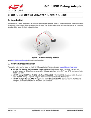
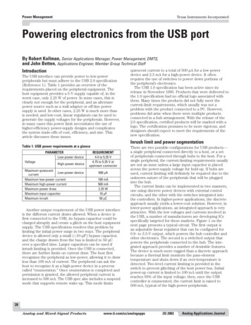
Power ManagementTexas Instruments IncorporatedPowering electronics from the USB portBy Robert Kollman, Senior Applications Manager, Power Management, DMTS,and John Betten, Applications Engineer, Member Group Technical Staffquiescent current to a total of 500 µA for a low-powerIntroductionThe USB interface can provide power to low-powerperipherals but must adhere to the USB 2.0 specification(Reference 1). Table 1 provides an overview of therequirements placed on the peripheral equipment. Thehost equipment provides a 5-V supply capable of, in theworst case, only 2.25 W of power. In some cases, this isclearly not enough for the peripheral, and an alternatepower source such as a wall adapter or off-line powersupply is used. In other cases, 2.25 W is much more thanis needed; and low-cost, linear regulators can be used togenerate the supply voltages for the peripherals. However,in many cases this power limit necessitates the use ofhigher-efficiency power-supply designs and complicatesthe system trade-offs of cost, efficiency, and size. Thisarticle discusses these issues.device and 2.5 mA for a high-power device. It oftenrequires the use of switches to power down portions ofthe peripheral’s electronics.The USB 1.0 specification has been active since itsrelease in November 1995. Products that were delivered tothe 1.0 specification had no official logo associated withthem. Many times the products did not fully meet thecurrent-limit requirements, which usually was not aproblem with the product connected to a PC. However,problems did arise when there were multiple productsconnected in a hub arrangement. With the release of the2.0 specification, certified products will be marked with alogo. The certification promises to be more rigorous, anddesigners should expect to meet the requirements of thenew specification.Inrush limit and power segmentationTable 1. USB power requirements at a glancePARAMETERLow-power deviceVoltageHigh-power deviceMaximum quiescentLow-power devicecurrentMaximum low-power currentMaximum high-power currentMaximum power drawMaximum input capacitorMaximum inrushREQUIREMENT4.4 to 5.25 V4.75 to 5.25 V atupstream connector500 µA100 mA500 mA2.25 W10 µF50 µCAnother unique requirement of the USB power interfaceis the different current draws allowed. When a device isfirst connected to the USB, its bypass capacitor could becharged abruptly and create a glitch on the host equipmentsupply. The USB specification resolves this problem bylimiting the initial power surge in two ways. The peripheraldevice is allowed only a small ( 10-µF) bypass capacitor,and the charge drawn from the bus is limited to 50 µCover a specified time. Larger capacitors can be used ifinrush limiting is provided. Once the USB is connected,there are further limits on current draw. The host firstrecognizes the peripheral as low-power, allowing it to drawless than 100 mA of current. The peripheral can ask thehost to recognize it as a high-power device in a processcalled “enumeration.” Once enumeration is completed andpermission is granted, the allowed peripheral current isincreased to 500 mA. The USB spec also includes a suspendmode that supports remote wake-up. This mode limitsThere are two possible configurations for USB products—a single peripheral connected directly to a host, or a setof peripherals connected through hubs to the host. For asingle peripheral, the current-limiting requirements usuallyare not an issue unless a large input capacitor is placedacross the power-supply voltage for hold-up. If hubs areused, current limiting will definitely be required due to theunknown nature of the peripherals that will be pluggedinto the hub.The current limits can be implemented in two manners,one using discrete power devices with external controlcircuits, and the other with the switches integrated intothe controllers. In higher-power applications, the discreteapproach usually yields a lower-cost solution. However, inlower-power applications, an integrated approach is veryattractive. With the low voltages and currents involved inthe USB, a number of manufacturers are developing ICsspecifically targeted for these markets. Figure 1 on thenext page presents a typical circuit. The first output isan adjustable linear regulator that can be configured for0.9- to 3.3-V output, which powers the hub controller andother electronics. The second is a switched output thatpowers the peripherals connected to the hub. The integrated approach provides a number of desirable features.The device is much more rugged than a discrete approachbecause a thermal limit monitors the pass-elementtemperature and shuts down if an over-temperature isdetected. Two-level current limiting is provided in theswitch to prevent glitching of the host power bus. Initialpower-up current is limited to 100 mA until the outputreaches 93% of the input voltage; then, once the USBcontroller is enumerated, the current limit is raised to500 mA, typical of the high-power peripherals.28Analog and Mixed-Signal Productswww.ti.com/sc/analogapps2Q 2002Analog Applications Journal
Power ManagementTexas Instruments IncorporatedFigure 1. Internal switch power segmentation and limitingU1TPS2140PWPBusPower2 C14.7 OPLDNLDOENAADJGNDLDOPG14Powerto OtherPeripherals1312C30.1 µF11 C44.7 µF1098R2332 kΩ15C20.1 µFSWPGPWP1SwitchEnableR1100 kΩC60.1 µF C54.7 µFPowerto HubControlTable 2. Power-management optionsPOWERMANAGERIMPLEMENTATIONInternal switchExternal switchSWITCHRESISTANCE(mΩ)10050CIRCUIT AREA(in2)0.300.5Table 2 compares the two approaches, internal versusexternal switches or pass elements. The pass elementshave higher resistance in the internal switch approach,which occupies less than 60% of the external switchapproach. However, the silicon die area is more costly inthe internal switch because more mask levels are involvedin the IC’s device structure than in a simple MOSFET.Typically, the IC will use over 20 mask levels comparedwith 8–10 levels of the MOSFET. The higher level of integration eliminates at least two semiconductor packagesand the resulting poor interconnect efficiency. In addition,the higher level of integration provides a higher reliabilityas bond wires and solder joints are eliminated. Reliabilityis further enhanced with the over-temperature protectionof the internal switch. With the external switch, there isno cost-effective method to measure MOSFET temperature to protect it from shorted loads. Current foldback andpower cycling techniques can help but do not provide therobustness of the thermal shutdown. The last column ofthe table presents a cost comparison between the twoapproaches. The costs are almost the same and wouldbear a closer examination on a particular requirement.Generally, the reason the costs are so close is that theOVERTEMPERATUREPROTECTIONYesNoOVERALLRELATIVE COST(%)80100external switch approach uses multiple semiconductorpackages compared with the single package of the integrated switch. Each of the packages has its own overheadof assembly and test, making the overall system-level costsabout equivalent.Powering low-voltage digital electronicsGenerating low voltages, such as 3.3 V, from the USB canbe done in several ways. Regardless of the configurationused, the output current for a 3.3-V output is limited to0.65 A (assuming 95% efficiency) due to the 2.25-W inputpower limitation. The options to provide these lower voltages include linear regulators, switching power supplies,and charge pumps. Within switching power supplies, thereare two further subgroups, synchronous and conventional.The synchronous is more efficient and costly and will beused to get as much power from the USB as possible.The linear regulator is the lowest-cost and highestdensity option for generating lower voltages from the 5-VUSB. When there is no power issue, it will be the circuitof choice. However, when power becomes an issue,switching regulators can more efficiently power the29Analog Applications Journal2Q 2002www.ti.com/sc/analogappsAnalog and Mixed-Signal Products
Power ManagementTexas Instruments Incorporatedperipheral. Figure 2 shows one of the lowest-cost buckswitching regulator options available. In this circuit, theswitching of the FET, Q2, is controlled to “buck” theaverage voltage presented to the output filter, which thensmooths the switching waveform. The drawback of thiscircuit is that the lack of controller integration requires anexternal FET and drive circuit, which makes the circuitrelatively large. An external FET provides flexibility in thedesign, allowing lower on resistance devices to be usedcompared with integrated FET controllers, and possiblyachieving greater efficiency.In Figure 2, a large percentage of the overall power lossis dissipated in the freewheeling diode D2. In Figure 3 thisdiode is replaced with an N-channel FET, making thiscircuit a synchronous buck converter, which significantlyimproves the converter efficiency. Efficiency improvementsFigure 2. Low-cost, non-synchronous buck regulator5 VIN 2VCC6DTC3R230.1 kΩR610 kΩOUT4FB7RT8 GNDR4100 kΩR543.2 kΩ3 2 1COMPC30.033 µFQ12N3904R1499 ΩU1TL5001DC2100 pFC1470 µF6.3 VSCP14Q2TPS1101D1MBRM1405L147 µH8 7 6 53.3 VD2MBRS340T3C41 µFR3100 kΩ C5470 µF6.3 VC61000 pFFigure 3. External-switch synchronous buck regulatorQ1Si3443DV5 VIN4C322 µF6.3 V3U1TPS43000R237.4 kΩC83.0 pFR532.4 MPVOUTFBC7270 pFR4115 kΩVPCCMVINC9560 pF3.3 V6521 C1120 µF4VC222 µF6.3 VR11 kΩ161514131211109R3L15.0 µH1 2 5 6C40.47 µF34C50.47 µFQ2Si3442DVD1ZHCS2000C60.47 µF5.76 kΩR6100 kΩ30Analog and Mixed-Signal Productswww.ti.com/sc/analogapps2Q 2002Analog Applications Journal
Power ManagementTexas Instruments IncorporatedFigure 4. Step-down charge pumpFigure 5. Boost regulator5 VINU1TPS60501DGSC11 µF16 V12345ENFBPGGNDC2F–C1F–C2F OUTVINC1F R1499 kΩ109876C2.01 µFC21 µF16 VC3.01 µFC422 µF6.3 VC34.7 µF6.3 V4ENVCCREFFBSSOUTCOMPGNDL115 µH876512 VD1MBRS130T3C510 µF16 Vsolution. The controller utilizes internal FETs that connecttwo flying capacitors in various series or parallel configurations, dumping their energy to the output. The inputvoltage and the load are used to set the internal FETconfiguration automatically. At loads heavier than 150 mA,the controller acts as an LDO and stops using the switchedcapacitors altogether. Output current is limited to a maximum of 0.25 A, which limits this circuit to low-powerapplications. Efficiency is between 80 and 90% for lightloads between 1 mA and 50 mA, but drops off to approximately 65% above that when operating in LDO mode. Thecost of Figure 4 is one of the lowest, due to the low cost ofthe ceramic capacitors.Table 3 provides a summary of the low-voltage step-downoptions discussed. Efficiency, cost, and circuit area arealso listed for reference. So what’s the right choice? Linearregulators, when you can afford the losses. Then take alook at charge pumps and determine their losses based onconversion ratios. Finally, evaluate non-synchronous andthen synchronous regulators. In each case, the systemcost and size increase, but more power is available for theload. A second trade-off in the switching power suppliesinvolves deciding between internal and external FETs.The cost is usually lowest with external FETs; while thedesign time, component count, and size will be smallerwith internal FETs.Powering higher-voltage analogTable 3. Low-voltage (5-V to 3.3-V) regulator optionsLinearNon-synchronous buckNon-synchronous buckSynchronous buckSynchronous buckCharge pump*2U1TPS6734DC41000 pFcan be realized over a wide load range with this circuit. Atvery light loads, pulse skipping can decrease gate-drivelosses. When the output voltage drops 2% below the nominal voltage set point, the converter senses it and switchesuntil the output reaches an upper threshold; it then putsitself in sleep mode until the load discharges the outputcapacitor to the lower threshold again. This circuit providesexcellent efficiency but is more costly than the one inFigure 2. Its circuit area is also slightly smaller, mainlybecause the controller can operate at frequencies of up to1 MHz, which allows the inductor and input/output capacitors to be noticeably smaller.Integrating the top FET, bottom FET, drive circuit, andfeedback compensation into the controller provides for asmall, integrated, and efficient converter solution. This isbecoming a very popular solution because it is generallysimple to design and has a very short design cycle time.Software is available that aids in the design, making itpossible for novices to design power supplies. Controllerssuch as the TPS5431x and TPS5461x SWIFT TM series provide such integration, but their cost is higher due to theadded performance and features.Circuit area is often a critical design parameter. The stepdown charge pump in Figure 4 represents an extremelysmall solution. Four ceramic capacitors and the chargepump controller are the only components required for thisTOPOLOGY133.3 V5 VININTERNALSWITCHYNYNYYC14.7 µF6.3 CIENCY(%)668785969560 to 90AREA(in2)0.11.21.11.00.70.15Higher-legacy voltages, such as 5 Vand 12 V, are often required to poweranalog circuits. The loading on theseoutputs is typically not as heavy as ontheir digital voltage counterparts—usually less than 100 mA. The circuitin Figure 5 is a boost regulator thatprovides 12 V and will provide up to120 mA while operating over the 5-VUSB output voltage range. In this*Current is limited to 0.25 A, and efficiency is largely dependent on input voltage.31Analog Applications Journal2Q 2002www.ti.com/sc/analogappsAnalog and Mixed-Signal Products
Power ManagementTexas Instruments IncorporatedFigure 6. Synchronous SEPIC converter5 VINC122 µF6.3 VD1B240L147 µHC31 µF1Q1IRF74042345 VOUT1 2 35 6 7 856Q2IRF74014781 2 3C622 µF6.3 VC7100 µF6.3 VR286.6 kΩU1UCC39421PWR31 kΩ5 6 7 84C21 µFR110 TSYNC/SDISENSE1615141311C81 µFC91 µFR528 kΩ109L247 µHR70.1 Ω0.25 WR4169 kΩ12R6169 kΩC468 pFC54700 pFD2BAT54R83.01 kΩdesign, the FET is integratedFigure 7. Synchronous buck converter with auxiliary output windinginto the controller along withthe feedback resistor network,reducing total parts count to aminimum. A drawback to thisQ1IRLMS6702approach is that the circuit5Vblock provides no current limit.U1If the 12-V output is shorted toC1TPS62000DGS10 µFground, there is nothing in the101VINPGND6.3 V5 VINVIN, L1, D1 path to limit current.29FCL3.3 VAn alternative topology, the38L1GNDENSEPIC, can overcome this shortC410µHC3C247R1PGSYNC10 µF0.1 µF4.7 µFcoming. Also, the SEPIC conver825 kΩ56FBILIM6.3 V6.3Vsion ratio extends above andbelow the input voltage ascompared with the boost, whoseR2130 kΩratio just includes voltage greaterthan VIN. Since the USB voltagecan range from 4.5 V to 5.5 V,the SEPIC converter in Figure 6makes an excellent choice for a5-V output. This SEPIC uses a synchronous rectifier Q1 tohigh RMS ripple-current rating and a low ESR to minimizereduce the losses in the output diode and improve effithe output ripple voltage. Ceramic capacitors are usuallyciency by several percent. Diode D1 conducts only duringchosen due to their high ripple-current rating and low cost.the on/off transitions of Q1 to prevent the intrinsic diodeFigure 7 shows an option for providing dual-output voltof Q1 from conducting. Additional benefits include lowages from a single synchronous buck converter. When theinput ripple currents and inherent current limiting. On thebottom-side FET (internal to TPS62000) conducts, FETnegative side, the addition of the dc blocking capacitor C3Q1 turns on, and output cap C1 charges with an additionalis required. Since the blocking capacitor and output capacivoltage developed across the secondary of L1. The level oftors must handle large pulsing currents, they require athe auxiliary voltage is determined by the turns ratio32Analog and Mixed-Signal Productswww.ti.com/sc/analogapps2Q 2002Analog Applications Journal
Power ManagementTexas Instruments IncorporatedTable 4. Higher-voltage regulator optionsTOPOLOGY5-V to 12-V boost5-V to 12-V boost5-V to 5-V SEPIC*5-V to 5-V SEPIC3.3-V to 5-V charge pump**Sync buck w/aux winding INTERNALSWITCHNYNYYY-Sync buckN-AuxTYPICALEFFICIENCY(%)8685898565 to 560550200100AREA(in2)0.70.61.00.90.20.3* Synchronous operation** TPS60133 charge pump controller, 0.3-A maximum output current Cost and area of auxiliary output onlybetween the two windings of L1. The voltage across C1 isstacked on the 3.3-V regulated output; so, for a 5-V auxiliaryoutput, an additional 1.7 V needs to be developed acrossL1’s secondary. A turns ratio of 2:1 will work well in thisapplication. For low current levels, the voltage dropsdeveloped across the internal bottom FET and Q1 (whichturn on in phase with each other) are small and often cancel each other out. These FET drops may not significantlyadd to the output-voltage tolerance error, and good regulation can be achieved.Table 4 presents a comparison of some of the optionsfor generating higher voltages for analog loads. Here again,the decision involves a trade-off between cost, performance,and loss. If power is not a problem, the first choice toconsider is a charge pump. When loss becomes an issue, aswitching regulator may become warranted. The firstcircuit to consider, particularly if a buck regulator is beingused, is the auxiliary winding scheme of Figure 7. It addsminimal cost and degrades efficiency the least. Next comethe SEPIC and boost regulator. The need for short-circuitprotection will determine which approach will be favored.Usually a boost will be chosen for its higher efficiency ifcurrent limiting is not needed or can be accommodatedelsewhere in the system. There are also trade-offs insynchronous and non-synchronous operation, as well as inan internal versus external switch, as in the buck regulator.USB-powered DSL modem power supply exampleThe circuit in Figure 8 (next page) is an example of acomplete USB power supply with 3.3-V, 5-V, and 12-Voutputs. With the 3.3-V powered at 0.32 A, the 5-V at0.05 A, and the 12-V at 0.05 A, the overall efficiency is89.5%, which allows the input power to remain below the2.25-W maximum limit. In operation, only the 3.3-V outputis allowed to power up at turn-on, with the 5-V and 12-Venable pins being held low by the bus controller. No morethan 100 mA is drawn off the 3.3-V output during powerup in low-power mode. Enumeration then comes from thebus controller to allow the 5-V and 12-V to power up. Aboost topology was used for both the 5-V and 12-V outputs,with the 5-V power stage input powered from the 3.3-Voutput. The controller chosen for both boost regulatorswas the low-cost TL1451A dual controller. The approachtaken for this design example is geared toward low costand high efficiency rather than small area. Figure 9 showsa photograph of the completed hardware, which measures1.5" 2".Figure 9. DSL modem power supply33Analog Applications Journal2Q 2002www.ti.com/sc/analogappsAnalog and Mixed-Signal Products
Power ManagementTexas Instruments IncorporatedFigure 8. USB-powered DSL modem power supplyJ14.5 - 5.5 VINGNDU1TPS62000DGS5 VIN12C20.1 µFC14.7 µF6.3 VC50.1 µF12345109L8EN7SYNC6VINPGNDFCGNDPGFBL110 µHJ24R3825 kΩILIMR6100 kΩR5130 kΩC60.1 µF3C410 µF6.3 VR7100 kΩ21Q1IRLMS6802R810 kΩ1 2 5 6Q32N70025-V & 12-VEnableC70.1 µFC80.1 µFR1010 kΩR1110 kΩGND12 V @ 100 mAQ2IRLMS68023R910 kΩ5 V @ 100 mA4433.3 V @ 500 mA1 2 5 6Q42N7002C94.7 µF6.3 VL23.8 µHR1384.5 kΩC140.1 µFC150.1 µFR2112.7 kΩR2320 kΩR22100 kΩR25C18.01 µFR181 kΩR2420 kΩU2TL1451ACNSC16.01 µFR2012.7 kΩR1920 kΩR261 kΩC111 µFR1528.0 kΩC130.1 µF100 kΩR2720 kΩ1611121314654321R2813.3 kΩVREF2DTC2FBGND2IN–2IN 2OUT1DTC1FB1OUTR161 2 5 631 kΩ9Q6MMBT3906R17499 Ω841IN RTSCPD1MBRS130T3Q7IRLMS2002C1210 µF16 VQ8MMBT3906107L310 µHC174.7 µF6.3 V15CTC191 µFC201 µFR301 kΩR29499 ΩQ9MMBT39041 2 5 63Q10MMBT3906R31499 ΩR3410 kΩQ5MMBT39041IN–C22150 pFC241 µFVCCR14499 Ω4D2MBRS130T3Q11IRLMS2002C2110 µF16 VQ12MMBT3906R3284.5 kΩConclusionReferenceThe design of a power supply powered from the USB portis heavily driven by the 2.25 W of available input powerand the peripheral load requirements. The design processshould involve a very careful analysis of load currentsfollowed by a program to minimize them. Once the loadshave been determined, the power-supply engineer shoulddevelop multiple block diagrams with the topologiesdescribed in this article to develop the lowest-cost, mostpower- and area-compliant approach. The array of integrated circuits to support these designs is very diverse;the designer has the options of striving for maximumintegration, minimum cost, and ease of use.1. USB Implementers Forum Inc., “Universal Serial BusSpecification Revision 2.0,” www.usb.orgRelated Web siteswww.ti.com/sc/device/partnumberReplace partnumber with TL1451A, TL5001, TPS2140,TPS6734, TPS43000, TPS54310, TPS54610, TPS54611,TPS60130, TPS60500, TPS62000 or UCC39421www.usb.org34Analog and Mixed-Signal Productswww.ti.com/sc/analogapps2Q 2002Analog Applications Journal
IMPORTANT NOTICETexas Instruments Incorporated and its subsidiaries (TI) reservethe right to make corrections, modifications, enhancements,improvements, and other changes to its products and services atany time and to discontinue any product or service without notice.Customers should obtain the latest relevant information beforeplacing orders and should verify that such information is currentand complete. All products are sold subject to TI's terms andconditions of sale supplied at the time of order acknowledgment.TI warrants performance of its hardware products to thespecifications applicable at the time of sale in accordance with TI'sstandard warranty. Testing and other quality control techniques areused to the extent TI deems necessary to support this warranty.Except where mandated by government requirements, testing ofall parameters of each product is not necessarily performed.TI assumes no liability for applications assistance or customerproduct design. Customers are responsible for their products andapplications using TI components. To minimize the risksassociated with customer products and applications, customersshould provide adequate design and operating safeguards.TI does not warrant or represent that any license, either express orimplied, is granted under any TI patent right, copyright, mask workright, or other TI intellectual property right relating to anycombination, machine, or process in which TI products or servicesare used. Information published by TI regarding third-partyproducts or services does not constitute a license from TI to usesuch products or services or a warranty or endorsement thereof.Use of such information may require a license from a third partyunder the patents or other intellectual property of the third party, or alicense from TI under the patents or other intellectual property of TI.Reproduction of information in TI data books or data sheets ispermissible only if reproduction is without alteration and isaccompanied by all associated warranties, conditions, limitations,and notices. Reproduction of this information with alteration is anunfair and deceptive business practice. TI is not responsible orliable for such altered documentation.Resale of TI products or services with statements different from orbeyond the parameters stated by TI for that product or servicevoids all express and any implied warranties for the associated TIproduct or service and is an unfair and deceptive businesspractice. TI is not responsible or liable for any such statements.Following are URLs where you can obtain information on otherTexas Instruments products and application solutions:ProductsAmplifiersData ConvertersDSPInterfaceLogicPower otiveBroadbandDigital controlMilitaryOptical NetworkingSecurityTelephonyVideo & ti.com/wirelessTI Worldwide Technical SupportInternetTI Semiconductor Product Information Center Home Pagesupport.ti.comTI Semiconductor KnowledgeBase Home Pagesupport.ti.com/sc/knowledgebaseProduct Information CentersAmericasPhoneInternet/Email 1(972) e, Middle East, and AfricaPhoneBelgium (English) 32 (0) 27 45 54 32Netherlands (English)Finland (English) 358 (0) 9 25173948RussiaFrance 33 (0) 1 30 70 11 64SpainGermany 49 (0) 8161 80 33 11Sweden (English)Israel (English)1800 949 0107United KingdomItaly800 79 11 37Fax (49) (0) 8161 80 iaPhoneInternationalDomesticAustraliaChinaHong KongIndonesiaKoreaMalaysiaFaxInternet 81-3-3344-5317Domestic 1(972) 927-6377 31 (0) 546 87 95 45 7 (0) 95 7850415 34 902 35 40 28 46 (0) 8587 555 22 44 (0) 1604 66 33 ij.co.jp/pic 886-2-23786800Toll-Free upport.ti.com/sc/pic/asia.htmNew -Free 011905Safe Harbor Statement: This publication may contain forwardlooking statements that involve a number of risks anduncertainties. These “forward-looking statements” are intendedto qualify for the safe harbor from liability established by thePrivate Securities Litigation Reform Act of 1995. These forwardlooking statements generally can be identified by phrases suchas TI or its management “believes,” “expects,” “anticipates,”“foresees,” “forecasts,” “estimates” or other words or phrasesof similar import. Similarly, such statements herein that describethe company's products, business strategy, outlook, objectives,plans, intentions or goals also are forward-looking statements.All such forward-looking statements are subject to certain risksand uncertainties that could cause actual results to differmaterially from those in forward-looking statements. Pleaserefer to TI's most recent Form 10-K for more information on therisks and uncertainties that could materially affect future resultsof operations. We disclaim any intention or obligation to updateany forward-looking statements as a result of developmentsoccurring after the date of this publication.Trademarks: SWIFT is a trademark of Texas Instruments. Allother trademarks are the property of their respective owners.Mailing Address:Texas InstrumentsPost Office Box 655303Dallas, Texas 75265 2005 Texas Instruments IncorporatedSLYT118
Low-power device 4.4 to 5.25 V Voltage High-power device 4.75 to 5.25 V at upstream connector Maximum quiescent Low-power device 500 µA current Maximum low-power current 100 mA Maximum high-power current 500 mA Maximum power draw 2.25 W Maximum input capacitor 10 µF Maximum inrush 50 µC Table 1. USB power requirements at a glance
