Transcription
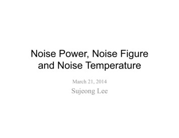
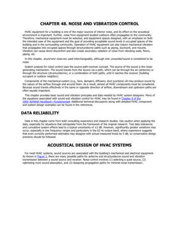
LTC6244Dual 50MHz, Low Noise,Rail-to-Rail, CMOS Op AmpFEATURESDESCRIPTIONnThe LTC 6244 is a dual high speed, unity-gain stable CMOSop amp that features a 50MHz gain bandwidth, 40V/μs slewrate, 1pA of input bias current, low input capacitance andrail-to-rail output swing. The 0.1Hz to 10Hz noise is just1.5μVP-P and 1kHz noise is guaranteed to be less than12nV/ Hz. This excellent AC and noise performance iscombined with wide supply range operation, a maximumoffset voltage of just 100μV and drift of only 2.5μV/ C,making it suitable for use in many fast signal processingapplications, such as photodiode amplifiers.nnnnnnnnnInput Bias Current: 1pA (Typ at 25 C)Low Offset Voltage: 100μV MaxLow Offset Drift: 2.5μV/ C Max0.1Hz to 10Hz Noise: 1.5μVP-PSlew Rate: 40V/μsGain Bandwidth Product: 50MHzOutput Swings Rail-to-RailSupply Operation:2.8V to 6V LTC62442.8V to 5.25V LTC6244HVLow Input Capacitance: 2.1pFAvailable in 8-Pin MSOP and Tiny DFN PackagesAPPLICATIONSnnnnnnPhotodiode AmplifiersCharge Coupled AmplifiersLow Noise Signal ProcessingActive FiltersMedical InstrumentationHigh Impedance Transducer AmplifierThis op amp has an output stage that swings within 35mVof either supply rail to maximize the signal dynamic rangein low supply applications. The input common moderange extends to the negative supply. It is fully specifiedon 3V and 5V, and an HV version guarantees operationon supplies of 5V.The LTC6244 is available in the 8-pin MSOP, and for compact designs, it is packaged in the tiny dual fine pitch leadfree (DFN) package.L, LT, LTC, LTM, Linear Technology and the Linear logo are registered trademarks of LinearTechnology Corporation. All other trademarks are the property of their respective owners.TYPICAL APPLICATIONVery Low Noise Large Area PhotodiodeVOS 7μF*IPD4.99kVBB901M5V4.99k1101/2LTC6244HV VOUT 1M IPDBW 350kHzNOISE 291nV AT 10kHzVOUTNUMBER OF UNITS5VLTC6244MS8VS 5V, 0VVCM 2.5VTA 25 C807060504030–5V 6244 TA01a2010HAMAMATSU LARGE AREAPHOTODIODES1227-1010BQCPD 3000pF0–602040–40 –200INPUT OFFSET VOLTAGE (μV)606244 TA01b* CAN BE MICROPHONIC, FILM, X7R, IF NEEDED.6244fb1
LTC6244ABSOLUTE MAXIMUM RATINGS (Note 1)Total Supply Voltage (V to V–)LTC6244.7VLTC6244HV .12VInput Voltage. (V 0.3V) to (V– – 0.3V)Input Current. 10mAOutput Short Circuit Duration (Note 2). IndefiniteOperating Temperature RangeLTC6244C . –40 C to 85 CLTC6244I. –40 C to 85 CLTC6244H . –40 C to 125 CSpecified Temperature Range (Note 3)LTC6244C . 0 C to 70 CLTC6244I. –40 C to 85 CLTC6244H . –40 C to 125 CJunction Temperature . 150 CStorage Temperature Range. –65 C to 150 CLead Temperature (Soldering, 10 sec) . 300 CPIN CONFIGURATIONTOP VIEW9OUT A 1–IN A 2 IN A 3V– 48 V TOP VIEW7 OUT BABOUT A–IN A IN AV–6 –IN B5 IN B12348765V OUT B–IN B IN BMS8 PACKAGE8-LEAD PLASTIC MSOPDD PACKAGE8-LEAD (3mm 3mm) PLASTIC DFNTJMAX 150 C, θJA 43 C/WEXPOSED PAD (PIN 9) CONNEECTED TO V–(PCB CONNECTION OPTIONAL)TJMAX 150 C, θJA 250 C/WORDER INFORMATIONLEAD FREE FINISHTAPE AND REELPART MARKINGPACKAGE DESCRIPTIONSPECIFIED TEMPERATURE RANGELTC6244CDD#PBFLTC6244CDD#TRPBFLCCF8-Lead (3mm 3mm) Plastic DFN0 C to 70 CLTC6244HVCDD#PBFLTC6244HVCDD#TRPBFLCGD8-Lead (3mm 3mm) Plastic DFN0 C to 70 CLTC6244IDD#PBFLTC6244IDD#TRPBFLCCF8-Lead (3mm 3mm) Plastic DFN–40 C to 85 CLTC6244HVIDD#PBFLTC6244HVIDD#TRPBFLCGD8-Lead (3mm 3mm) Plastic DFN–40 C to 85 CLTC6244HDD#PBFLTC6244HDD#TRPBFLCCF8-Lead (3mm 3mm) Plastic DFN–40 C to 125 CLTC6244HVHDD#PBFLTC6244HVHDD#TRPBFLCGD8-Lead (3mm 3mm) Plastic DFN–40 C to 125 CLTC6244CMS8#PBFLTC6244CMS8#TRPBFLTCCM8-Lead Plastic MSOP0 C to 70 CLTC6244HVCMS8#PBFLTC6244HVCMS8#TRPBF LTCGF8-Lead Plastic MSOP0 C to 70 CLTC6244IMS8#PBFLTC6244IMS8#TRPBFLTCCM8-Lead Plastic MSOP–40 C to 85 CLTC6244HVIMS8#PBFLTC6244HVIMS8#TRPBFLTCGF8-Lead Plastic MSOP–40 C to 85 CLTC6244HMS8#PBFLTC6244HMS8#TRPBFLTCCM8-Lead Plastic MSOP–40 C to 125 CConsult LTC Marketing for parts specified with wider operating temperature ranges.Consult LTC Marketing for information on non-standard lead based finish parts.For more information on lead free part marking, go to: http://www.linear.com/leadfree/For more information on tape and reel specifications, go to: http://www.linear.com/tapeandreel/6244fb2
LTC6244ELECTRICAL CHARACTERISTICS(LTC6244C/I, LTC6244HVC/I) The l denotes the specifications which applyover the specified temperature range, otherwise specifications are at TA 25 C. VS 5V, 0V, VCM 2.5V unless otherwise noted.SYMBOLPARAMETERCONDITIONSVOSInput Offset Voltage (Note 4)MS8 Package0 C to 70 C–40 C to 85 CllDD Package0 C to 70 C–40 C to 85 CllVOS Match Channel-to-Channel (Note 5) MS8 Package0 C to 70 C–40 C to 85 CllDD Package0 C to 70 C–40 C to 85 CllTC VOSInput Offset Voltage Drift, MS8 (Note 6)IBInput Bias Current (Notes 4, 72.5μV/ C75pApA75pApA1lInput Offset Current (Notes 4, 7)TYP0.5lInput Noise Voltage0.1Hz to 10HzenInput Noise Voltage Densityf 1kHzinInput Noise Current Density (Note 8)0.56fA/ HzRINInput ResistanceCommon Mode1012ΩCINInput CapacitanceDifferential ModeCommon Modef 100kHz3.52.1pFpFVCMInput Voltage RangeGuaranteed by CMRRl0CMRRCommon Mode Rejection0V VCM 3.5Vl74105dBCMRR MatchChannel-to-Channel (Note 5)AVOLLarge Signal Voltage Gain1.58μVP-P123.5nV/ HzVl72100dBVO 1V to 4VRL 10k to VS/20 C to 70 C–40 C to 85 Cll10006004502500V/mVV/mVV/mVVO 1.5V to 3.5VRL 1k to VS/20 C to 70 C–40 C to 85 Cll3002001501000V/mVV/mVV/mVVOLOutput Voltage Swing Low (Note 9)No LoadISINK 1mAISINK 5mAlll15401503575300mVmVmVVOHOutput Voltage Swing High (Note 9)No LoadISOURCE 1mAISOURCE 5mAlll15451753575325mVmVmVPSRRPower Supply RejectionVS 2.8V to 6V, VCM 0.2Vl75105dBPSRR MatchChannel-to-Channel (Note 5)l73100dBMinimum Supply Voltage (Note 10)l2.8ISCShort-Circuit Currentl25ISSupply Current per AmplifierlV356.25mA7.4mA6244fb3
LTC6244ELECTRICAL CHARACTERISTICS(LTC6244C/I, LTC6244HVC/I) The l denotes the specifications which applyover the specified temperature range, otherwise specifications are at TA 25 C. VS 5V, 0V, VCM 2.5V unless otherwise in Bandwidth ProductFrequency 100kHz, RL 1kΩl3550MHzSRSlew Rate (Note 11)AV –2, RL 1kΩl1835V/μsFPBWFull Power Bandwidth (Note 12)VOUT 3VP-P, RL 1kΩl1.93.7MHztsSettling TimeVSTEP 2V, AV –1, RL 1kΩ, 0.1%535ns(LTC6244C/I, LTC6244HVC/I) The l denotes the specifications which apply over the specified temperature range, otherwisespecifications are at TA 25 C. VS 3V, 0V, VCM 1.5V unless otherwise noted.SYMBOLPARAMETERCONDITIONSVOSInput Offset Voltage (Note 4)MS8 Package0 C to 70 C–40 C to 85 CllDD Package0 C to 70 C–40 C to 85 CllVOS Match Channel-to-Channel (Note 5) MS8 Package0 C to 70 C–40 C to 85 CllDD Package0 C to 70 C–40 C to 85 CllIBIOSInput Bias Current (Notes 4, 7)MIN0.1Hz to 10HzenInput Noise Voltage Densityf 1kHzinInput Noise Current Density (Note 5lInput Noise VoltageMAX401lInput Offset Current (Notes 4, 7)TYP1.58μVP-P120.56nV/ HzfA/ HzVCMInput Voltage RangeGuaranteed by CMRRlCMRRCommon Mode Rejection0V VCM 1.5Vl70105dBCMRR MatchChannel-to-Channel (Note 5)AVOLLarge Signal Voltage Gain01.5Vl68100dBVO 1V to 2VRL 10k to VS/20 C to 70 C–40 C to 85 Cll20010085800V/mVV/mVV/mVVOLOutput Voltage Swing Low (Note 9)No LoadISINK 1mAll124530110mVmVVOHOutput Voltage Swing High (Note 9)No LoadISOURCE 1mAll125030110mVmVPSRRPower Supply RejectionVS 2.8V to 6V, VCM 0.2VlISCPSRR MatchChannel-to-Channel (Note 5)Minimum Supply Voltage (Note 10)Short-Circuit Current75105dBl73100dBl2.8l8V15mA6244fb4
LTC6244ELECTRICAL CHARACTERISTICS(LTC6244C/I, LTC6244HVC/I) The l denotes the specifications which applyover the specified temperature range, otherwise specifications are at TA 25 C. VS 3V, 0V, VCM 1.5V unless otherwise noted.SYMBOLPARAMETERISSupply Current per AmplifierGBWGain Bandwidth ProductCONDITIONSMINlFrequency 100kHz, RL 1kΩl35TYPMAX4.85.850UNITSmAMHz(LTC6244HVC/I) The l denotes the specifications which apply over the specified temperature range, otherwise specifications are atTA 25 C. VS 5V, 0V, VCM 0V unless otherwise noted.SYMBOLPARAMETERCONDITIONSVOSInput Offset Voltage (Note 4)MS8 Package0 C to 70 C–40 C to 85 CllDD Package0 C to 70 C–40 C to 85 CllVOS Match Channel-to-Channel (Note 5) MS8 Package0 C to 70 C–40 C to 85 CllDD Package0 C to 70 C–40 C to 85 CllTC VOSInput Offset Voltage Drift, MS8 (Note 6)IBInput Bias Current (Notes 4, �V0.72.5μV/ C75pApA75pApA1lInput Offset Current (Notes 4, 7)TYP0.5lInput Noise Voltage0.1Hz to 10HzenInput Noise Voltage Densityf 1kHzinInput Noise Current Density (Note 8)0.56fA/ HzRINInput ResistanceCommon Mode1012ΩCINInput CapacitanceDifferential ModeCommon Modef 100kHz3.52.1pFpFVCMInput Voltage RangeGuaranteed by CMRRl–5CMRRCommon Mode Rejection–5V VCM 3.5Vl80105dBl7895dBVO –3.5V to 3.5VRL 10k0 C to 70 C–40 C to 85 Cll2500150012006000V/mVV/mVV/mVRL 1k0 C to 70 C–40 C to 85 Cll7004003003500V/mVV/mVV/mVCMRR MatchChannel-to-Channel (Note 5)AVOLLarge Signal Voltage Gain1.58μVP-P123.5nV/ HzVVOLOutput Voltage Swing Low (Note 9)No LoadISINK 1mAISINK 10mAlll15453604075550mVmVmVVOHOutput Voltage Swing High (Note 9)No LoadISOURCE 1mAISOURCE 10mAlll15453604075550mVmVmV6244fb5
LTC6244ELECTRICAL CHARACTERISTICS(LTC6244HVC/I) The l denotes the specifications which apply over thespecified temperature range, otherwise specifications are at TA 25 C. VS 5V, 0V, VCM 0V unless otherwise noted.SYMBOLPSRRPARAMETERMINTYPl75110dBPSRR MatchChannel-to-Channel (Note 5)l73106dB2.84055mAPower Supply RejectionCONDITIONSVS 2.8V to 10.5V, VCM 0.2VMinimum Supply Voltage (Note 10)lISCShort-Circuit CurrentlISSupply Current per AmplifierlGBWGain Bandwidth ProductFrequency 100kHz, RL 1kΩSRSlew Rate (Note 11)MAXUNITSV78.8mAl3550MHzAV –2, RL 1kΩl1840V/μsl1.94.25MHz330nsFPBWFull Power Bandwidth (Note 12)VOUT 3VP-P, RL 1kΩtsSettling TimeVSTEP 2V, AV –1, RL 1kΩ, 0.1%(LTC6244H) The l denotes the specifications which apply from –40 C to 125 C, otherwise specifications are at TA 25 C. VS 5V, 0V,VCM 2.5V unless otherwise noted.SYMBOLPARAMETERCONDITIONSVOSInput Offset Voltage (Note 4)MS8 PackageDD8 PackageVOS Match Channel-to-Channel (Note 5) MS8 PackageDD8 Package–40 C to 125 CTC VOSInput Offset Voltage Drift, MS8 (Note 6)IBInput Bias Current (Notes 4, 40160400μVμV1508001160μVμV0.72.51lInput Offset Current (Notes 4, 7)TYP2pAnA250pApA3.5V0.5lμV/ CVCMInput Voltage RangeGuaranteed by CMRRl0CMRRCommon Mode Rejection0V VCM 3.5Vl74dBl72dBVO 1V to 4VRL 10k to VS /2l350V/mVVO 1.5V to 3.5VRL 1k to VS /2l125CMRR MatchChannel-to-Channel (Note 5)AVOLLarge Signal Voltage GainV/mVVOLOutput Voltage Swing Low (Note 9)No LoadISINK 1mAISINK 5mAlll4085325mVmVmVVOHOutput Voltage Swing High (Note 9)No LoadISOURCE 1mAISOURCE 5mAlll4085325mVmVmV6244fb6
LTC6244ELECTRICAL CHARACTERISTICS(LTC6244H) The l denotes the specifications which apply from –40 C to125 C, otherwise specifications are at TA 25 C. VS 5V, 0V, VCM 2.5V unless otherwise Bl2.8VShort-Circuit Currentl20mAISSupply Current per AmplifierlGBWGain Bandwidth ProductFrequency 100kHz, RL 1kΩSRSlew Rate (Note 11)AV –2, RL 1kΩl17V/μsFPBWFull Power Bandwidth (Note 12)VOUT 3VP-P, RL 1kΩl1.8MHzPSRRPower Supply RejectionPSRR MatchChannel-to-Channel (Note 5)Minimum Supply Voltage (Note 10)ISCVS 2.8V to 6V, VCM 0.2VMINll6.257.430mAMHz(LTC6244H) The l denotes the specifications which apply from –40 C to 125 C, otherwise specifications are at TA 25 C. VS 3V, 0V,VCM 1.5V unless otherwise noted.SYMBOLPARAMETERCONDITIONSVOSInput Offset Voltage (Note 4)MS8 PackageDD8 PackageVOS Match Channel-to-Channel (Note 5) MS8 PackageDD8 PackageIBIOSInput Bias Current (Notes 4, 0400μVμV1508001200μVμV2pAnA250pApA1lInput Offset Current (Notes 4, 7)TYP0.5lVCMInput Voltage RangeGuaranteed by CMRRl0CMRRCommon Mode Rejection0V VCM 1.5Vl70dBdBCMRR MatchChannel-to-Channel (Note 5)1.5Vl68AVOLLarge Signal Voltage GainVO 1V to 2VRL 10k to VS /2l75VOLOutput Voltage Swing Low (Note 9)No LoadISINK 1mAll30110mVmVVOHOutput Voltage Swing High (Note 9)No LoadISOURCE 1mAll30110mVmVPSRRPower Supply RejectionVS 2.8V to 6V, VCM 0.2Vl75dBPSRR Match Channel-to-Channel(Note 5)l73dB2.85Minimum Supply Voltage (Note 10)lISCShort-Circuit CurrentlISSupply Current per AmplifierlGBWGain Bandwidth ProductFrequency 100kHz, RL 1kΩlV/mVVmA4.8285.8mAMHz6244fb7
LTC6244ELECTRICAL CHARACTERISTICS(LTC6244HVH) The l denotes the specifications which apply from –40 C to125 C, otherwise specifications are at TA 25 C. VS 5V, VCM 0V unless otherwise noted.SYMBOLPARAMETERCONDITIONSVOSInput Offset Voltage (Note 4)DD8 PackageVOS Match Channel-to-Channel (Note 5) DD8 PackageTC VOSInput Offset Voltage Drift, MS8 (Note 6)IBInput Bias Current (Notes 4, V0.72.51lInput Offset Current (Notes 4, 7)TYP2pAnA250pAnA0.5lμV/ CInput Noise Voltage0.1Hz to 10HzenInput Noise Voltage Densityf 1kHzinInput Noise Current Density (Note 8)0.56fA/ HzRINInput ResistanceCommon Mode1012ΩCINInput CapacitanceDifferential ModeCommon Modef 100kHz3.52.1pFpFVCMInput Voltage RangeGuaranteed by CMRRl–5CMRRCommon Mode Rejection–5V VCM 0V/mVV/mVCMRR MatchChannel-to-Channel (Note 5)AVOLLarge Signal Voltage GainVO –3.5V to 3.5VRL 10kRL 1k1.58μVP-P123.5nV/ HzVVOLOutput Voltage Swing Low (Note 9)No LoadISINK 1mAISINK 10mAlll15453604075550mVmVmVVOHOutput Voltage Swing High (Note 9)No LoadISOURCE 1mAISINK 10mAlll15453604075550mVmVmVPSRRPower Supply RejectionVS 2.8V to 10.5V, VCM 0.2Vl75110dBPSRR Match Channel-to-Channel(Note 5)l73106dBMinimum Supply Voltage (Note 10)l2.8ISCShort-Circuit Currentl4055VlmAISSupply Current per AmplifierGBWGain Bandwidth ProductFrequency 100kHz, RL 1kΩl35509.3MHzmASRSlew Rate (Note 11)AV –2, RL 1kΩl1840V/μsFPBWFull Power Bandwidth (Note 12)VOUT 3VP-P, RL 1kΩl1.94.3MHztsSettling TimeVOUT 2V, AV –1 , RL 1kΩl330ns6244fb8
LTC6244ELECTRICAL CHARACTERISTICSNote 1: Stresses beyond those listed under Absolute Maximum Ratingsmay cause permanent damage to the device. Exposure to any AbsoluteMaximum Rating condition for extended periods may affect devicereliability and lifetime.Note 2: A heat sink may be required to keep the junction temperaturebelow the absolute maximum rating when the output is shortedindefinitely.Note 3: The LTC6244C/LTC6244HVC are guaranteed to meet specifiedperformance from 0 C to 70 C. They are designed, characterized andexpected to meet specified performance from –40 C to 85 C, but are nottested or QA sampled at these temperatures. The LTC6244I/LTC6244HVI,are guaranteed to meet specified performance from –40 C to 85 C. TheLTC6244H is guaranteed to meet specified performance from –40 C to125 C.Note 4: ESD (Electrostatic Discharge) sensitive device. ESD protectiondevices are used extensively internal to the LTC6244; however, highelectrostatic discharge can damage or degrade the device. Use proper ESDhandling precautions.Note 5: Matching parameters are the difference between the two amplifiersof the LTC6244. CMRR and PSRR match are defined as follows: CMRRand PSRR are measured in μV/V on the amplifiers. The difference iscalculated between the sides in μV/V. The result is converted to dB.Note 6: This parameter is not 100% tested.Note 7: This specification is limited by high speed automated testcapability. See Typical Characteristics curves for actual typicalperformance.Note 8: Current noise is calculated from the formula: in (2qIB)1/2where q 1.6 10–19 coulomb. The noise of source resistors up to50GΩ dominates the contribution of current noise. See also TypicalCharacteristics curve Noise Current vs Frequency.Note 9: Output voltage swings are measured between the output andpower supply rails.Note 10: Minimum supply voltage is guaranteed by the power supplyrejection ratio test.Note 11: Slew rate is measured in a gain of –2 with RF 1k and RG 500Ω. VIN is 1V and VOUT slew rate is measured between –1V and 1V.On the LTC6244HV/LTC6245HV, VIN is 2V and VOUT slew rate is measuredbetween –2V and 2V.Note 12: Full-power bandwidth is calculated from the slew rate:FPBW SR/2πVP.6244fb9
LTC6244TYPICAL PERFORMANCE CHARACTERISTICSVOS Distribution60120LTC6244MS8VS 5V, 0VVCM 2.5VTA 25 C10050NUMBER OF UNITSNUMBER OF UNITS90LTC6244DDVS 5V, 0VVCM 2.5VTA 25 C8070605040NUMBER OF UNITS110VOS Temperature CoefficientDistributionVOS Distribution403020301020100–602040–40 –200INPUT OFFSET VOLTAGE (μV)60–500 –350 –200 –50 100 250INPUT OFFSET VOLTAGE (μV)VOS Temperature CoefficientDistribution7654385007400630054322TA 125 CTA 25 CTA –55 C110–6 –5 –4 –3 –2 –1 0 1 2 3DISTRIBUTION (μV/ C)45060248106TOTAL SUPPLY VOLTAGE (V)6422 G041000800700TA 125 C600100TA 85 C10TA 25 C10–100–200TA 125 CTA 25 CTA –55 C–300–400–1 –0.5 0 0.5 1 1.5 2 2.5 3 3.5 4 4.5 5INPUT COMMON MODE VOLTAGE (V)6244 G061 1.5 2 2.5 3 3.5 4 4.5COMMON MODE VOLTAGE (V)56244 G07Input Bias Current vs TemperatureMS8 PACKAGEVS 5V, 0VMS8 PACKAGEVCM 000200Input Bias Currentvs Common Mode VoltageINPUT BIAS CURRENT (pA)INPUT BIAS CURRENT (pA)MS8 PACKAGEVS 5V, 0V12VS 5V, 0VNORMALIZED TO25 C VOS VALUE6244 G05Input Bias Currentvs Common Mode Voltage10000Offset Voltagevs Input Common Mode VoltageOFFSET VOLTAGE (μV)SUPPLY CURRENT (mA)NUMBER OF UNITS982.46422 G03Supply Current vs Supply Voltage(Per Amplifier)LTC6244DDVS 5V, 0VVCM 2.5V2 LOTS–55 C TO 125 C101.66244 G026244 G0111400INPUT BIAS CURRENT (pA)01413 LTC6244MS8VS 5V, 0V12VCM 2.5V11 2 LOTS10 –55 C TO 125 C9876543210–2.4 –1.6 –0.800.8DISTRIBUTION (μV/ C)TA 125 CTA 25 C100010010VS 10VVS 5V1TA 85 C–400–0.8 –0.6 –0.4 –0.2 0 0.2 0.4 0.6 0.8 1.0COMMON MODE VOLTAGE (V)6244 G080.125 35 45 55 65 75 85 95 105 115 125TEMPERATURE ( C)6244 G096244fb10
LTC6244TYPICAL PERFORMANCE CHARACTERISTICSOutput Saturation Voltagevs Load Current (Output Low)1010.1TA 125 CTA 25 CTA –55 C0.1110LOAD CURRENT (mA)VS 5V10.1TA 125 CTA 25 CTA –55 C0.010.1100110LOAD CURRENT 0VS 5VVS L SUPPLY VOLTAGE (V)28–5012AV 10.01100M6244 G16VS 5VVS 2.5VRISING5025075TEMPERATURE ( C)–256244 G14Channel Separation vs Frequency9080706050403020TA 25 C–10 V 2.5VS–20 AV 0–1010k100k1M10MFREQUENCY (Hz)1250TA 25 CVS 2.5V1001006244 G15CHANNEL SEPARATION (dB)AV 2FALLING3830COMMON MODE REJECTION RATIO (dB)OUTPUT IMPEDANCE (Ω)101M10MFREQUENCY (Hz)44Common Mode Rejection Ratiovs Frequency100100kAV –248 RF 1k, RG 500Ω46 CONDITIONS: SEE NOTE 11GAIN BANDWIDTH50–120100MTA 25 CVS 2.5VAV 105 25 45 65 85 105 125TEMPERATURE ( C)5050401101VS 1.5VSlew Rate vs TemperaturePHASE MARGINOutput Impedance vs Frequency0.00110kCL 5pFRL 1k–1001M10MFREQUENCY (Hz)0.1VS 5V50606244 G1310006030–55 –35 –15PHASE MARGIN (DEG)7050–20GAINBANDWIDTH6244 G12TA 25 CCL 5pFRL 1kPHASE (DEG)GAIN (dB)80120CL 5pF100RL 1kVCM VS/2 80200Gain Bandwidth and PhaseMargin vs Supply VoltageGAIN BANDWIDTH (MHz)9040VS 1.5V6244 G11Open Loop Gain vs Frequency6070401006244 G10100PHASEMARGINSLEW RATE (V/μs)0.0180VS 5V, 0VGAIN BANDWIDTH (MHz)OUTPUT HIGH SATURATION VOLTAGE (V)VS 5V, 0VGain Bandwidth and PhaseMargin vs TemperaturePHASE MARGIN (DEG)OUTPUT LOW SATURATION VOLTAGE (V)10Output Saturation Voltagevs Load Current (Output High)100M6244 G17–12010k1001M10MFREQUENCY (Hz)100M6244 G186244fb11
LTC6244TYPICAL PERFORMANCE CHARACTERISTICSPower Supply Rejection Ratiovs 200150100500–50–100–150TA 125 CTA 25 CTA –55 C–200–250–300–101k10k100k1MFREQUENCY (Hz)10M100M012 3 4 5 6 7 8TOTAL SUPPLY VOLTAGE (V)6244 G19–60–70RL 10k–80RL 1k–90–1004TA 25 CVS 5V, 0V–60–70RL 10k–80RL 1k–90–301.5 2 2.5 3 3.5 4OUTPUT VOLTAGE (V)–5CHANGE IN OFFSET VOLTAGE (μV)–50TA –55 C–1506244 G25–60–70RL 100k–80RL 10k–9004.5 50.521.51OUTPUT VOLTAGE (V)6244 G24VS 1.5V–20VS 5V–25–30TA 25 CVS 2.5VVCM 0V35–15VS 2.5V–35–4540TA 25 C–1032.5Noise Voltage vs Frequency30252015105–40– 200–50 –40 –30 –20 –10 0 10 20 30 40 50OUTPUT CURRENT (mA)5TA 25 CVS 3V, 0V–50Warm-Up Drift vs TimeVS 5VTA 25 C3.532.544.5POWER SUPPLY VOLTAGE ( V)6244 G23Offset Voltage vs Output CurrentTA 125 C2–1100 0.5 16244 G22100TA 125 CTA 25 CTA –55 C–40–100–1105150SOURCING–206244 G21NOISE VOLTAGE (nV/ Hz)2 3–5 –4 –3 –2 –1 0 1OUTPUT VOLTAGE (V)OFFSET VOLTAGE p Gain–50INPUT VOLTAGE (μV)INPUT VOLTAGE (μV)–50–10020–40–40TA 25 CVS 5V030Open-Loop Gain–4050406244 G20Open-Loop Gain2009INPUT VOLTAGE (μV)7050VCM VS/2250OUTPUT SHORT-CIRCUIT CURRENT (mA)9080300TA 25 CVS 2.5VCHANGE IN OFFSET VOLTAGE (μV)POWER SUPPLY REJECTION RATIO (dB)100Output Short-Circuit Currentvs Power Supply VoltageMinimum Supply Voltage005 10 15 20 25 30 35 40 45 50 55 60TIME AFTER POWER UP (SEC)6244 G26101001k10kFREQUENCY (Hz)100k6244 G276244fb12
LTC6244TYPICAL PERFORMANCE CHARACTERISTICS0.1Hz to 10Hz Voltage NoiseSeries Output Resistance andOvershoot vs Capacitive LoadNoise Current vs Frequency100060TA 25 CVS 2.5VVCM 0VVOUT 100mVVS 2.5VAV –25030pF10040OVERSHOOT (%)NOISE CURRENT (fA/ Hz)VOLTAGE NOISE (500nV/DIV)VS 5V, 0V101k30RS 10Ω– 500ΩRSCL20110RS 50Ω0.1100TIME (1s/DIV)01k10kFREQUENCY (Hz)6244 G2860501k30– VOUT 100mVVS 2.5VAV 1900VS 5V800 AV 1TA 25 C700RS 10ΩRSCL20RS 50Ω10SETTLING TIME (ns)401k4030RS 50Ω20– 10100CAPACITIVE LOAD (pF)101000100CAPACITIVE LOAD 2OUTPUT STEP (V)36244 G3441mV10mV–4–3–201–12OUTPUT STEP (V)34Distortion vs Frequency–30–4087654AV 232–41k1mV6244 G339OUTPUT VOLTAGE SWING (VP-P)SETTLING TIME (ns)1k6004000100010– VOUT300Maximum Undistorted OutputSignal vs Frequency9001kVIN400– 6244 G32Settling Timevs Output Step (Inverting)VIN5001006244 G31VS 5V800 AV –1TA 25 C70060010mVCLVS 5VTA 25 CHD2, HD3 –40dBc110kAV –1100k1MFREQUENCY (Hz)DISTORTION (dBc)10NOTE: EXCEEDS INPUTCOMMON MODE RANGE200RS000Settling Timevs Output Step (Noninverting)RS 10ΩOVERSHOOT (%)OVERSHOOT (%)30pF10006244 G30Series Output Resistance andOvershoot vs Capacitive LoadVOUT 100mVVS 2.5VAV –150100CAPACITIVE LOAD (pF)6244 G29Series Output Resistance andOvershoot vs Capacitive Load6010100kVS 2.5VAV 1VOUT 2VP-P–50RL 1k, 2ND–60–70–80RL 1k, 3RD–9010M6244 G35–10010k100k1MFREQUENCY (Hz)10M6244 G366244fb13
LTC6244TYPICAL PERFORMANCE CHARACTERISTICS–30–30–40–50–60RL 1k, 2ND–70RL 1k, 3RD–80VS 5VAV 1VOUT 2VP-P–40–50–60RL 1k, 2ND–70–80–90–90–10010k100k1MFREQUENCY (Hz)10MDISTORTION (dBc)VS 2.5VAV 2VOUT 2VP-PDISTORTION (dBc)DISTORTION (dBc)–40Distortion vs FrequencyDistortion vs FrequencyDistortion vs Frequency–30100k1MFREQUENCY (Hz)–50–60–8010MSmall-Signal Response–10010k200ns/DIV10MLarge-Signal ResponseSmall-Signal Response6244 G40100k1MFREQUENCY (Hz)6244 G390V0VVS 2.5VAV 1RL RL 1k, 3RD6244 G386244 G370VRL 1k, 2ND–70–90RL 1k, 3RD–10010kVS 5VAV 2VOUT 2VP-PVS 2.5VAV 1RL CL 75pF6244 G41200ns/DIVVS 5VAV 1RL 2μs/DIV6244 G42Output Overdrive RecoveryLarge-Signal ResponseVIN0V1V/DIV0VVOUT0V2V/DIVVS 2.5VAV –1RL 1k200ns/DIV6244 G43VS 2.5VAV 3RL 3k200ns/DIV6244 G446244fb14
LTC6244APPLICATIONS INFORMATIONAmplifier CharacteristicsESDFigure 1 is a simplified schematic of the LTC6244, whichhas a pair of low noise input transistors M1 and M2. Asimple folded cascode Q1, Q2 and R1, R2 allow the inputstage to swing to the negative rail, while performing levelshift to the Differential Drive Generator. Low offset voltageis accomplished by laser trimming the input stage.The LTC6244 has reverse-biased ESD protection diodes onall input and outputs as shown in Figure 1. These diodesprotect the amplifier for ESD strikes to 4kV. If these pinsare forced beyond either supply, unlimited current willflow through these diodes. If the current transient is lessthan 1 second and limited to one hundred milliamps orless, no damage to the device will occur.Capacitor C1 reduces the unity cross frequency and improves the frequency stability without degrading the gainbandwidth of the amplifier. Capacitor CM sets the overallamplifier gain bandwidth. The differential drive generatorsupplies signals to transistors M3 and M4 that swing theoutput from rail-to-rail.The photo of Figure 2 shows the output response to aninput overdrive with the amplifier connected as a voltagefollower. If the negative going input signal is less thana diode drop below V–, no phase inversion occurs. Forinput signals greater than a diode drop below V–, limit thecurrent to 3mA with a series resistor RS to avoid phaseinversion.The input common mode voltage range extends fromV– to V – 1.5V. In unity gain voltage follower applications,exceeding this range by applying a signal that reaches 1Vfrom the positive supply rail can create a low level instabilityat the output. Loading the amplifier with several hundredmicro-amps will reduce or eliminate the instability.The amplifier input bias current is the leakage current ofthese ESD diodes. This leakage is a function of the temperature and common mode voltage of the amplifier, asshown in the Typical Performance Chacteristics.NoiseThe LTC6244 exhibits low 1/f noise in the 0.1Hz to 10Hzregion. This 1.5μVP-P noise allows these op amps to beused in a wide variety of high impedance low frequencyapplications, where Zero-Drift amplifiers might be inappropriate due to their input sampling characteristic.In the frequency region above 1kHz the LTC6244 alsoshows good noise voltage performance. In this frequencyregion, noise can easily be dominated by the total sourceV 2.5VV V–ITAILV CMDESD1M3DESD2VIN 4V–V––2.5VV VODESD6C1 2.5VV–V BIASVOUT AND VIN OF FOLLOWER WITH LARGE INPUT OVERDRIVEV–Q1R1Q2RS0ΩVINR2V–6244 F01Figure 1. Simplified Schematic–M41/2LTC6244VOUT –2.5V6244 F02Figure 2. Unity Gain Follower Test Circuit6244fb15
LTC6244APPLICATIONS INFORMATIONresistance of the particular application. Specifically, theseamplifiers exhibit the noise of a 4k resistor, meaning it isdesirable to keep the source and feedback resistance at orbelow this value, i.e., RS RG RFB 4k. Above this totalsource impedance, the noise voltage is not dominated bythe amplifier.In low gain configurations and with RF and RS in eventhe kilohm range (Figure 3), this pole can create excessphase shift and possibly oscillation. A small capacitor CFin parallel with RF eliminates this problem.Noise current can be estimated from the expression in 2qIB, where q 1.6 10–19 coulombs. Equating 4kTRΔfand RS 2qIBΔf shows that for source resistors below50GΩ the amplifier noise is dominated by the sourceresistance. See the Typical Characteristics curve NoiseCurrent vs Frequency.The DD package is leadless and makes contact to the PCBbeneath the package. Solder flux used during the attachment of the part to the PCB can create leakage currentpaths and can degrade the input bias current performanceof the part. All inputs are susceptible because the backsidepaddle is connected to V– internally. As the input voltagechanges or if V– changes, a leakage path can be formedand alter the observed input bias current. For lowest biascurrent, use the LTC6244 in the MS8 package.Achieving Low Input Bias CurrentProprietary design techniques are used to obtain simultaneous low 1/f noise and low input capacitance. Low inputcapacitance is important when the amplifier is used withhigh source and feedback resistors. High frequency noisefrom the amplifier tail current source, ITAIL in Figure 1,couples through the input capacitance and appears acrossthese large source and feedback resistors.Photodiode AmplifiersPhotodiodes can be broken into two categories: large areaphotodiodes with their attendant high capacitance (30pFto 3000pF) and smaller area photodiodes with relativelylow capacitance (10pF or less). For optimal signal-to-noiseperformance, a transimpedance amplifier consisting of aninverting op amp and a feedback resistor is most commonlyused to convert the photodiode current into voltage. In lownoise amplifier design, large area photodiode amplifiersrequire more attention to reducing op amp input voltagenoise, while small area photodiode amplifiers requiremore attention to reducing op amp input current noiseand parasitic capacitances.StabilityThe good noise performance of these op amps can beattributed to large input devices in the differential pair.Above several hundred kilohertz, the input capacitancecan cause amplifier stability problems if left unchecked.When the feedback around the op amp is resistive (RF), apole will be created with RF, the source resistance, sourcecapacitance (RS, CS), and the amplifier input capacitance.CFRF–RSCINCSOUTPUT6244 F03 Figure 3. Compensating
Rail-to-Rail, CMOS Op Amp The LTC 6244 is a dual high speed, unity-gain stable CMOS op amp that features a 50MHz gain bandwidth, 40V/μs slew rate, 1pA of input bias current, low input capacitance and rail-to-rail output swing. The 0.1Hz to 10Hz noise is just 1.5μVP-P and 1kHz noise is guaranteed to be less than 12nV/ Hz.