Transcription
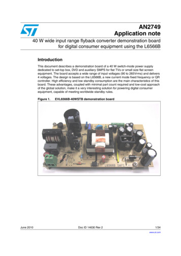
UM10572PCA9955 demonstration board OM13330Rev. 1 — 7 June 2012User manualDocument informationInfoContentKeywordsFm I2C-bus, PCA9955, RGB and white LEDs, 16-channel 8-bit PWMsAbstractThe OM13330 is an add-on to 9-pin connector of the NXP I2C demo board2005-1 or Fm I2C-bus development board. This daughter board makes iteasy to test and design with the PCA9955, a 16-channel Fast-mode Plus(Fm ) 57 mA constant current and outputs allow up to 40 V for LEDsupply. These boards, along with the Win-I2CUSB Lite GUI (PC based),provide an easy to use evaluation platform.
UM10572NXP SemiconductorsPCA9955 demonstration board OM13330Revision historyRevDateDescriptionv.120120607user manual; initial releaseContact informationFor more information, please visit: http://www.nxp.comFor sales office addresses, please send an email to: salesaddresses@nxp.comUM10572User manualAll information provided in this document is subject to legal disclaimers.Rev. 1 — 7 June 2012 NXP B.V. 2012. All rights reserved.2 of 16
UM10572NXP SemiconductorsPCA9955 demonstration board OM133301. IntroductionThe PCA9955 evaluation board features LEDs for color mixing, blinking and dimmingdemonstrations. A graphical interface allows the easy exploration of the different functionsof the driver. The board can be connected in series with other I2C-bus demo boards tocreate an evaluation system.The IC communicates to the host via the industry standard I2C-bus/SMBus port. Theevaluation software runs under Microsoft Windows PC platform.2. Features A complete evaluation platform for the PCA9955 16-channel Fm I2C-bus constantcurrent LED driver Easy to use GUI-based software demonstrates the capabilities of the PCA9955On-board RGB and White LEDs for visual experienceConvenient test points for easy scope measurements and signal accessUSB interface to the host PCNo external power supply required3. Getting started3.1 AssumptionsFamiliarity with the I2C-bus is helpful but not required.3.2 Static handling requirementsCAUTIONThis device is sensitive to ElectroStatic Discharge (ESD). Therefore care should be takenduring transport and handling. You must use a ground strap or touch the PC case or othergrounded source before unpacking or handling the hardware.3.3 Minimum system requirements PC Pentium 60 processor (or equivalent), 8 MB RAM, 10 MB of hard drive spaceOne USB port (either 2.0 or 1.1 compatible)Windows 98SE, ME, 2000, XP, or VistaI2C demonstration board 2005-1 (OM6275) or WIN-I2CUSB board (fromwww.nxp.com/redirect/demoboard.com)3.4 Power requirementsThe NXP demonstration board I2C 2005-1 and OM13330 hardware obtain power from thePC USB port. Take care to not exceed the USB port current capabilities.UM10572User manualAll information provided in this document is subject to legal disclaimers.Rev. 1 — 7 June 2012 NXP B.V. 2012. All rights reserved.3 of 16
UM10572NXP SemiconductorsPCA9955 demonstration board OM133304. Installation4.1 I2C demo board 2005-1 and WIN-I2CUSB Lite softwareThe OM13330 is a daughter card to the OM6275 I2C demo board 2005-1. You candownload the WIN-I2CUSB Lite Software, the OM6275 user manual UM10206, and findordering information at the NXP web site ics.nxp.com/support/boards/i2c20051/.The Win-I2CUSB Lite software from The Boardshop runs on Windows 98SE, ME, 2000,and XP, and is compatible with any PC hardware having a minimum of a Pentiumprocessor and a USB port. The software allows the user to select one of the I2C-busdevices on the board from a menu and also provides a Universal mode (I2C Expert mode)to allow users to create their own I2C-bus commands with the same I2C-bus devices.4.2 OM13330 connection to I2C demo board 2005-1The I2C demo board 2005-1 should be disconnected from your PC before mounting theOM13330 board on to it. The OM13330 board has a 9-pin female connector (J4) thatconnects to the JP1 male connector on the I2C demo board 2005-1 as shown in Figure 1.With both boards facing you, with USB connector on the right-hand side as shown in theFigure 1, connect the OM13330 board to the I2C demo board 2005-1 before connectingthe USB cable. Once the board is connected, connect the USB cable and start theWIN-I2CUSB Lite software. You are now ready to evaluate the PCA9955.Fig 1.PCA9955 demo board (OM13330) mounting to the I2C demo board 2005-1 (OM6275)UM10572User manualAll information provided in this document is subject to legal disclaimers.Rev. 1 — 7 June 2012 NXP B.V. 2012. All rights reserved.4 of 16
UM10572NXP SemiconductorsPCA9955 demonstration board OM133304.3 OM13330 connection to Win-I2CUSB hardware adapter boardThe Win-I2CUSB board should be disconnected from your PC before connecting theOM13330 board on to it. The OM13330 board has a 14-pin male connector (J2) thatconnects to the 14-pin male connector (J1) on the Win-I2CUSB board as shown inFigure 2.Connect the OM13330 board to the Win-I2CUSB board before connecting the USB cable.Once the board is connected, connect the USB cable and start the WIN-I2CUSB Litesoftware. You are now ready to evaluate the PCA9955.Fig 2.PCA9955 demo board (OM13330) connecting to the Win-I2CUSB boardUM10572User manualAll information provided in this document is subject to legal disclaimers.Rev. 1 — 7 June 2012 NXP B.V. 2012. All rights reserved.5 of 16
UM10572NXP SemiconductorsPCA9955 demonstration board OM133305. Hardware descriptionFig 3.PCA9955 demo board (OM13330)Figure 3 shows the following items on the hardware: J4 (9-pin) is for connection to JP1 on I2C demo board 2005-1. J3 and J5 (5-pin) are for connection to PCA9665/PCU9669 mini boards and cascadethe second PCA9955 demo board. J1 selects VDD power for PCA9955, connected 1-2 for VDD 3.3 V and connected 2-3for VDD 5 V. SW1 4-position DIP switch to select I2C-bus address A[0:3] SW1[1:4] for this device(default is 0xC0, all switches are ON position). J2 (14-pin) is for connection to J1 on Win-I2CUSB board. 4-channel to drive four White LEDs (D2, D4, D6, D9) and 12-channel to drivefour RGB LEDs (D3, D5, D7, D8). J6, J7 and J8 are GND pins for probing use.UM10572User manualAll information provided in this document is subject to legal disclaimers.Rev. 1 — 7 June 2012 NXP B.V. 2012. All rights reserved.6 of 16
xxxx xxxxxxxxxxxxxxxxxxxxxxxxxxxxxx x xxxxxxxxxxxxxx xxxxxxxxxx xxx xxxxxx xxxxxxxxxxxxxxxxxxxxxxx xxxxxxxxxxxxxxxxxxxxxxxxxxx xxxxxx xx xxxxxxxxxxxxxxxxxxxxxxxxxxxxx xxxxxxxxxxxxxxxxxxxxxx xxxxxxxxxxx xxxxxxx xxxxxxxxxxxxxxxxxxxxxxxxxxxxxxxxxxx xxxxxxxxxxxxxx xxxxxx xx xxxxxxxxxxxxxxxxxxxxxxxxxxxxxxxx xxxxxxxxxxxxxxxxxxxxxxxx xxx xxxxxxxxxxx xxxxx x xRev. 1 — 7 June 20125-pin connector to/from PCU9669 UFmI2C master board to drive PCU9955 orto/from another I2C slave PCA/PCU9955demo boardJ512345 24 V 5 VSDA USDA 2SCL USCL 2GND123do not populateJ7R12U12345J3CONN TRBLK-5RV1D1LTST-C170KGKT9-pin connector to/from I2C 2005-1demo board for PCA9952/PCA9955CON9-female 5 V 3.3 VSCL USCL 1C610 μFPCA9952TW, PCA9955TW, PCU9955TWC810 μFC20.1 μF1 kΩR810 ΩC34.7 μFAVR-M1608C080MSDA USDA filterSCL USCL filter0Ω0Ωvaristor 8 LED9LED810 kΩ100 Ω100 ΩR62827262524232221201918171615100 ΩSW1SW 1LED5LED10LED6LED9LED7LED8100 3GNDLED4LED5LED6LED7(output enablefor PCA9952)C510 μFR510 kΩ10 kΩ10 kΩR4R3R92.8 kΩ 24 V 5 VSDA USDA 1C110 μF SCL USCL 1GNDC7GND10 μFSDA USDA 1321RESET123456789J4GND321 5 VCONN 3C240.1 nF 0.1 nF 0.1 nF 0.1 nF 0.1 nF 0.1 nF 0.1 nF 0.1 nF 0.1 nF 0.1 nF 0.1 nF 0.1 nF 0.1 nF 0.1 nF 0.1 nF 0.1 �2C1C3A3L1BLM18BD471SN1D7A1C2A2D8 I/O243LED4GND 5 VC250.01 μFSDA USDA-filterL2BLM18BD471SN1SCL USCL 1D5 LED[5:7]A1C2A2GNDPRTR5V0U2AXSDA USDA 1LRTB G6SG0ΩLED9LED10U21LW-E67C-whiteD3 LED[1:3]0ΩLED6LED7close to 5-pin connector J3D2LED0D4SCL USCL-filter(470 Ω at 100 MHz)LW-E67C-white321LRTB G6SGLED8close to 5-pin connector J5D6U31LW-E67C-white2LRTB G6SGLED12J6L3BLM18BD471SN1D9LW-E67C-whiteSDA USDA 2GNDVCCI/O1I/O2PRTR5V0U2AX43 5 VJ8GNDC260.01 μFSDA USDA-filterL4BLM18BD471SN1LRTB G6SGSCL USCL 2SCL USCL-filter019aac728Fig 4.PCA9955 demo board schematicUM105727 of 16 NXP B.V. 2012. All rights reserved.(470 Ω at 100 MHz)PCA9955 demonstration board OM13330All information provided in this document is subject to legal disclaimers.C410 μFHEADER 7x2/SMI2CUSB CONNECTORR2(ISET max 20.4 mA)TP1 5 VVDD INR13GND 3.3 V2468101214R1J2135791113VP supplies thepower to the I2Cpull-up resistorson WIN-I2CUSB(VP) VDO INSCL USCL 2GNDSDA USDA 210 kΩVDD IN14-pin connector to/fromWIN-I2CUSB Fm I2C masterto drive PCA9952/PCA99555-pin connector to/from PCU9669 UFmI2C master board to drive PCU9955 orto/from another I2C slave PCA/PCU9955demo board 5 VNXP Semiconductors 3.3 V6. SchematicUM10572User manualJ1
UM10572NXP SemiconductorsPCA9955 demonstration board OM133307. OM13330 demonstration board main componentsTable 1.OM13330 demo board main componentsDeviceDescriptionAddress/LED outputLocationPCA9955TW16-channel Fm I2C-bus 57 mAconstant current LED driver0xC0 for I2C demo board 2005-1interfaceU1LW-E67CWhite LEDLED0, LED4, LED8, LED12D2, D4, D6, D9LRTB G6SGRGB LEDLED1, LED2, LED3D3LRTB G6SGRGB LEDLED5, LED6, LED7D5LRTB G6SGRGB LEDLED9, LED10, LED11D7LRTB G6SGRGB LEDLED13, LED14, LED15D8LTST-C170KGKTGreen LED for PCA9955 power supplyeither 3.3 V or 5 V indicator-D18. PCA9955 evaluation stepsThe PCA9955 functions are controlled by WIN-I2CUSB Lite GUI. Refer to the PCA9955data sheet for additional information on the registers and functionality.Connect the hardware as described in Section 4. The PCA9955 demo board address isset to 0xC0 on SW1 as A[0:3] SW1[1:4] 0000 (0 ON, 1 OFF). When you havecorrectly installed the software and the demonstration board hardware is connected andrecognized by the computer, start the Win-I2CUSB Lite software. As shown in Figure 5,when the demonstration board hardware is correctly connected to the USB port and thecomputer recognizes it, the message ‘Hardware Detected’ is displayed on the bottom ofthe window.Switched 3.3 V and 5.0 V power supplies are controlled through the ‘Options’ menu or bydouble-clicking the 3.3 V or 5.0 V symbols on the bottom of the window. Power suppliesare disabled by default, and must be enabled before using the I2C-bus devices on theboard. I2C-bus frequency is controlled through the ‘Options’ menu or by double-clicking onthe frequency symbol on the bottom of the window.8.1 Color mixing and dimming LEDs1. From the ‘Device’ drop-down menus, select ‘LED Blinkers and Dimmers’, and fromthe subsequent drop-down menu select ‘PCA9955 16-channel Constant Current LEDDriver’ as shown in Figure 5.2. Check the ‘Auto Write On’ box (lower left), uncheck the ‘Low power mode (oscillatoroff)’ box to enable the device to ‘Normal mode’ (upper left).3. The device configuration screen is displayed by clicking the following options:– ‘PWM 0 to 7’ individual brightness control for LED0 to LED7 as shown in Figure 6.– ‘PWM 8 to 15’ individual brightness control for LED8 to LED15 as shown inFigure 7.– ‘LEDOUT’ LED driver output state for LED0 to LED15 as shown in Figure 8.– ‘Output Gain’ LED output current setting for LED0 to LED15 as shown in Figure 9.UM10572User manualAll information provided in this document is subject to legal disclaimers.Rev. 1 — 7 June 2012 NXP B.V. 2012. All rights reserved.8 of 16
UM10572NXP SemiconductorsPCA9955 demonstration board OM13330– ‘Other’ GRPPWM is group PWM for global brightness control, GRPFREQ is groupfrequency for global blinking control when group control blinking in Mode 2register, PWMALL is brightness control for all LED outputs, OFFSET is control LEDoutput delay offset, IREFALL is control output current for all LEDs as shown inFigure 10.4. Click the ‘LEDOUT’ configuration screen and select ‘PWMn & GRPPWM’ for LED[1:3](see Figure 8).5. Click the ‘Output Gain’ configuration screen and adjust the IREF[1:3] 0x30 forLED[1:3] output current at 3.8 mA 48 80 μA (see Figure 9).6. Click the ‘PWM 0 to 7’ configuration screen and move the PWM1 (red) PWM2 (green)PMW3 (blue) bars for color mixing (see Figure 6).7. Once you set a color on D3 RGB LED with the PWM[1:3] values, click the ‘Other’configuration screen and move the GRPPWM bar for dimming effect (see Figure 10).Fig 5.UM10572User manualDrop-down menu selectionsAll information provided in this document is subject to legal disclaimers.Rev. 1 — 7 June 2012 NXP B.V. 2012. All rights reserved.9 of 16
UM10572NXP SemiconductorsPCA9955 demonstration board OM13330UM10572User manualFig 6.Device configuration screen for PWM[0:7]Fig 7.Device configuration screen for PWM[8:15]All information provided in this document is subject to legal disclaimers.Rev. 1 — 7 June 2012 NXP B.V. 2012. All rights reserved.10 of 16
UM10572NXP SemiconductorsPCA9955 demonstration board OM13330UM10572User manualFig 8.Device configuration screen for LEDOUTFig 9.Device configuration screen for LED output current settingAll information provided in this document is subject to legal disclaimers.Rev. 1 — 7 June 2012 NXP B.V. 2012. All rights reserved.11 of 16
UM10572NXP SemiconductorsPCA9955 demonstration board OM13330Fig 10. Device configuration screen for ‘Other’ (Group and All registers)UM10572User manualAll information provided in this document is subject to legal disclaimers.Rev. 1 — 7 June 2012 NXP B.V. 2012. All rights reserved.12 of 16
UM10572NXP SemiconductorsPCA9955 demonstration board OM133308.2 Color mixing and blinking LEDsTo set up a blinking demo, repeat step 1 through step 7 as in Section 8.1, then do thefollowing:1. In the Mode 2 ( 0x25) selection window (middle left), check the‘Group control dimming’ box to change the mode to ‘Group control blinking’.2. To set a blink cycle, click the ‘Other’ configuration screen and move the GRPFREQbar to select blinking frequency as well as the GRPPWM bar to select the duty cycle(see Figure 11).3. For example, set the GRPPWM to 0x52 (32 % duty cycle) and the GRPFREQ to 0x0B(0.5 second) for a one-third duty cycle and blink every half second on D3 RGB LED.4. Change the PWM[1:3] values, GRPPWM and GRPFREQ values to create differentblink patterns and colors.Fig 11. Example of short blink every half second9. SupportFor support, send an E-mail to: i2c.support@nxp.comUM10572User manualAll information provided in this document is subject to legal disclaimers.Rev. 1 — 7 June 2012 NXP B.V. 2012. All rights reserved.13 of 16
UM10572NXP SemiconductorsPCA9955 demonstration board OM1333010. AbbreviationsTable 2.AbbreviationsAcronymDescriptionESDElectroStatic DischargeGUIGraphical User InterfaceI2C-busInter-Integrated Circuit busICIntegrated CircuitLEDLight-Emitting DiodePCPersonal ComputerPWMPulse Width ModulatorRAMRandom Access usSystem Management BusUSBUniversal Serial Bus11. ReferencesUM10572User manual[1]PCA9955, 16-channel Fm I2C-bus 57 mA constant current LED driver —Product data sheet; NXP Semiconductors;www.nxp.com/documents/data sheet/PCA9952 PCA9955.pdf[2]UM10206, “I2C Demonstration Board 2005-1 Quick Start Guide” —NXP Semiconductors; www.nxp.com/documents/user manual/UM10206.pdfAll information provided in this document is subject to legal disclaimers.Rev. 1 — 7 June 2012 NXP B.V. 2012. All rights reserved.14 of 16
UM10572NXP SemiconductorsPCA9955 demonstration board OM1333012. Legal information12.1 DefinitionsDraft — The document is a draft version only. The content is still underinternal review and subject to formal approval, which may result inmodifications or additions. NXP Semiconductors does not give anyrepresentations or warranties as to the accuracy or completeness ofinformation included herein and shall have no liability for the consequences ofuse of such information.12.2 DisclaimersLimited warranty and liability — Information in this document is believed tobe accurate and reliable. However, NXP Semiconductors does not give anyrepresentations or warranties, expressed or implied, as to the accuracy orcompleteness of such information and shall have no liability for theconsequences of use of such information. NXP Semiconductors takes noresponsibility for the content in this document if provided by an informationsource outside of NXP Semiconductors.In no event shall NXP Semiconductors be liable for any indirect, incidental,punitive, special or consequential damages (including - without limitation - lostprofits, lost savings, business interruption, costs related to the removal orreplacement of any products or rework charges) whether or not suchdamages are based on tort (including negligence), warranty, breach ofcontract or any other legal theory.Notwithstanding any damages that customer might incur for any reasonwhatsoever, NXP Semiconductors’ aggregate and cumulative liability towardscustomer for the products described herein shall be limited in accordancewith the Terms and conditions of commercial sale of NXP Semiconductors.Right to make changes — NXP Semiconductors reserves the right to makechanges to information published in this document, including withoutlimitation specifications and product descriptions, at any time and withoutnotice. This document supersedes and replaces all information supplied priorto the publication hereof.Suitability for use — NXP Semiconductors products are not designed,authorized or warranted to be suitable for use in life support, life-critical orsafety-critical systems or equipment, nor in applications where failure ormalfunction of an NXP Semiconductors product can reasonably be expectedto result in personal injury, death or severe property or environmentaldamage. NXP Semiconductors and its suppliers accept no liability forinclusion and/or use of NXP Semiconductors products in such equipment orapplications and therefore such inclusion and/or use is at the customer’s ownrisk.design. It is customer’s sole responsibility to determine whether the NXPSemiconductors product is suitable and fit for the customer’s applications andproducts planned, as well as for the planned application and use ofcustomer’s third party customer(s). Customers should provide appropriatedesign and operating safeguards to minimize the risks associated with theirapplications and products.NXP Semiconductors does not accept any liability related to any default,damage, costs or problem which is based on any weakness or default in thecustomer’s applications or products, or the application or use by customer’sthird party customer(s). Customer is responsible for doing all necessarytesting for the customer’s applications and products using NXPSemiconductors products in order to avoid a default of the applications andthe products or of the application or use by customer’s third partycustomer(s). NXP does not accept any liability in this respect.Export control — This document as well as the item(s) described hereinmay be subject to export control regulations. Export might require a priorauthorization from competent authorities.Evaluation products — This product is provided on an “as is” and “with allfaults” basis for evaluation purposes only. NXP Semiconductors, its affiliatesand their suppliers expressly disclaim all warranties, whether express, impliedor statutory, including but not limited to the implied warranties ofnon-infringement, merchantability and fitness for a particular purpose. Theentire risk as to the quality, or arising out of the use or performance, of thisproduct remains with customer.In no event shall NXP Semiconductors, its affiliates or their suppliers be liableto customer for any special, indirect, consequential, punitive or incidentaldamages (including without limitation damages for loss of business, businessinterruption, loss of use, loss of data or information, and the like) arising outthe use of or inability to use the product, whether or not based on tort(including negligence), strict liability, breach of contract, breach of warranty orany other theory, even if advised of the possibility of such damages.Notwithstanding any damages that customer might incur for any reasonwhatsoever (including without limitation, all damages referenced above andall direct or general damages), the entire liability of NXP Semiconductors, itsaffiliates and their suppliers and customer’s exclusive remedy for all of theforegoing shall be limited to actual damages incurred by customer based onreasonable reliance up to the greater of the amount actually paid by customerfor the product or five dollars (US 5.00). The foregoing limitations, exclusionsand disclaimers shall apply to the maximum extent permitted by applicablelaw, even if any remedy fails of its essential purpose.Translations — A non-English (translated) version of a document is forreference only. The English version shall prevail in case of any discrepancybetween the translated and English versions.Applications — Applications that are described herein for any of theseproducts are for illustrative purposes only. NXP Semiconductors makes norepresentation or warranty that such applications will be suitable for thespecified use without further testing or modification.12.3 TrademarksCustomers are responsible for the design and operation of their applicationsand products using NXP Semiconductors products, and NXP Semiconductorsaccepts no liability for any assistance with applications or customer productI2C-bus — logo is a trademark of NXP B.V.UM10572User manualNotice: All referenced brands, product names, service names and trademarksare the property of their respective owners.All information provided in this document is subject to legal disclaimers.Rev. 1 — 7 June 2012 NXP B.V. 2012. All rights reserved.15 of 16
UM10572NXP SemiconductorsPCA9955 demonstration board OM1333013. 12.112.212.313Introduction . . . . . . . . . . . . . . . . . . . . . . . . . . . . 3Features . . . . . . . . . . . . . . . . . . . . . . . . . . . . . . . 3Getting started . . . . . . . . . . . . . . . . . . . . . . . . . . 3Assumptions . . . . . . . . . . . . . . . . . . . . . . . . . . . 3Static handling requirements . . . . . . . . . . . . . . 3Minimum system requirements. . . . . . . . . . . . . 3Power requirements . . . . . . . . . . . . . . . . . . . . . 3Installation . . . . . . . . . . . . . . . . . . . . . . . . . . . . . 4I2C demo board 2005-1 and WIN-I2CUSB Litesoftware . . . . . . . . . . . . . . . . . . . . . . . . . . . . . . 4OM13330 connection toI2C demo board 2005-1 . . . . . . . . . . . . . . . . . . 4OM13330 connection to Win-I2CUSBhardware adapter board . . . . . . . . . . . . . . . . . . 5Hardware description . . . . . . . . . . . . . . . . . . . . 6Schematic . . . . . . . . . . . . . . . . . . . . . . . . . . . . . . 7OM13330 demonstration board maincomponents . . . . . . . . . . . . . . . . . . . . . . . . . . . . 8PCA9955 evaluation steps . . . . . . . . . . . . . . . . 8Color mixing and dimming LEDs . . . . . . . . . . . 8Color mixing and blinking LEDs . . . . . . . . . . . 13Support . . . . . . . . . . . . . . . . . . . . . . . . . . . . . . . 13Abbreviations . . . . . . . . . . . . . . . . . . . . . . . . . . 14References . . . . . . . . . . . . . . . . . . . . . . . . . . . . 14Legal information. . . . . . . . . . . . . . . . . . . . . . . 15Definitions . . . . . . . . . . . . . . . . . . . . . . . . . . . . 15Disclaimers . . . . . . . . . . . . . . . . . . . . . . . . . . . 15Trademarks. . . . . . . . . . . . . . . . . . . . . . . . . . . 15Contents . . . . . . . . . . . . . . . . . . . . . . . . . . . . . . 16Please be aware that important notices concerning this document and the product(s)described herein, have been included in section ‘Legal information’. NXP B.V. 2012.All rights reserved.For more information, please visit: http://www.nxp.comFor sales office addresses, please send an email to: salesaddresses@nxp.comDate of release: 7 June 2012Document identifier: UM10572
Mouser ElectronicsAuthorized DistributorClick to View Pricing, Inventory, Delivery & Lifecycle Information:NXP:OM13330 OM13330,598
The Win-I2CUSB board should be disconnected from your PC before connecting the OM13330 board on to it. The OM13330 board has a 14-pin male connector (J2) that connects to the 14-pin male connector (J1) on the Win-I2CUSB board as shown in Figure 2. Connect the OM13330 board to the Win-I2CU SB board before connecting the USB cable.