Transcription
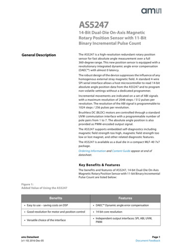
AN2749Application note40 W wide input range flyback converter demonstration boardfor digital consumer equipment using the L6566BIntroductionThis document describes a demonstration board of a 40 W switch-mode power supplydedicated to set-top box, DVD and auxiliary SMPS for flat TVs or small size flat screenequipment. The board accepts a wide range of input voltages (90 to 265Vrms) and delivers4 voltages. The design is based on the L6566B, a new current mode fixed frequency or QRcontroller. High efficiency and low standby consumption are the main characteristics of thisboard. These advantages, coupled with minimal part count required and low-cost approachof the global solution, make it a very interesting solution for powering digital consumerequipment, capable of meeting worldwide standby rules.Figure 1.June 2010EVL6566B-40WSTB demonstration boardDoc ID 14630 Rev 21/34www.st.com
ContentsAN2749Contents1Main characteristics . . . . . . . . . . . . . . . . . . . . . . . . . . . . . . . . . . . . . . . . . 42Circuit description . . . . . . . . . . . . . . . . . . . . . . . . . . . . . . . . . . . . . . . . . . . 63Functional checking . . . . . . . . . . . . . . . . . . . . . . . . . . . . . . . . . . . . . . . . . 93.1Full-load operation . . . . . . . . . . . . . . . . . . . . . . . . . . . . . . . . . . . . . . . . . . . 93.2Reduced load operation, without the HDD . . . . . . . . . . . . . . . . . . . . . . . . 113.3Minimum load operation . . . . . . . . . . . . . . . . . . . . . . . . . . . . . . . . . . . . . . 123.4Wakeup time and startup . . . . . . . . . . . . . . . . . . . . . . . . . . . . . . . . . . . . . 163.5Power down - hold-up time . . . . . . . . . . . . . . . . . . . . . . . . . . . . . . . . . . . . 183.6Overload and overcurrent protection (OCP) . . . . . . . . . . . . . . . . . . . . . . . 193.7Overvoltage protection (OVP) . . . . . . . . . . . . . . . . . . . . . . . . . . . . . . . . . 224Conducted noise measurements . . . . . . . . . . . . . . . . . . . . . . . . . . . . . . 235Thermal measures . . . . . . . . . . . . . . . . . . . . . . . . . . . . . . . . . . . . . . . . . . 246Bill of material . . . . . . . . . . . . . . . . . . . . . . . . . . . . . . . . . . . . . . . . . . . . . 257PCB layout . . . . . . . . . . . . . . . . . . . . . . . . . . . . . . . . . . . . . . . . . . . . . . . . 298Transformer specifications . . . . . . . . . . . . . . . . . . . . . . . . . . . . . . . . . . 309Conclusion . . . . . . . . . . . . . . . . . . . . . . . . . . . . . . . . . . . . . . . . . . . . . . . . 329.1102/34References . . . . . . . . . . . . . . . . . . . . . . . . . . . . . . . . . . . . . . . . . . . . . . . . 32Revision history . . . . . . . . . . . . . . . . . . . . . . . . . . . . . . . . . . . . . . . . . . . 33Doc ID 14630 Rev 2
AN2749List of figuresList of figuresFigure 1.Figure 2.Figure 3.Figure 4.Figure 5.Figure 6.Figure 7.Figure 8.Figure 9.Figure 10.Figure 11.Figure 12.Figure 13.Figure 14.Figure 15.Figure 16.Figure 17.Figure 18.Figure 19.Figure 20.Figure 21.Figure 22.Figure 23.Figure 24.Figure 25.Figure 26.Figure 27.Figure 28.Figure 29.Figure 30.Figure 31.Figure 32.Figure 33.Figure 34.Figure 35.Figure 36.Figure 37.Figure 38.Figure 39.EVL6566B-40WSTB demonstration board . . . . . . . . . . . . . . . . . . . . . . . . . . . . . . . . . . . . . . 1Electrical diagram . . . . . . . . . . . . . . . . . . . . . . . . . . . . . . . . . . . . . . . . . . . . . . . . . . . . . . . . . 5EVL6566B-40WSTB waveforms at 115 Vac-60 Hz - full load . . . . . . . . . . . . . . . . . . . . . . . 9EVL6566B-40WSTB waveforms at 230 Vac-50 Hz - full load . . . . . . . . . . . . . . . . . . . . . . . 9EVL6566B-40WSTB waveforms at 265 V-50 Hz - full load . . . . . . . . . . . . . . . . . . . . . . . . 10EVL6566B-40WSTB waveforms at 230 V - Pin 30 W . . . . . . . . . . . . . . . . . . . . . . . . . . . . 13EVL6566B-40WSTB waveforms at 230 V - Pin 4 W . . . . . . . . . . . . . . . . . . . . . . . . . . . . 13EVL6566B-40WSTB waveforms at 265 Vac - no load . . . . . . . . . . . . . . . . . . . . . . . . . . . . 14EVL6566B-40WSTB waveforms at 265 Vac - no load (detail) . . . . . . . . . . . . . . . . . . . . . . 14Input power vs. mains voltage during standby . . . . . . . . . . . . . . . . . . . . . . . . . . . . . . . . . . 15Pin at 230 Vac vs. Iout 5 V . . . . . . . . . . . . . . . . . . . . . . . . . . . . . . . . . . . . . . . . . . . . . . . . . 15EVL6566B-40WSTB wakeup time at 115 Vac . . . . . . . . . . . . . . . . . . . . . . . . . . . . . . . . . . 16EVL6566B-40WSTB wakeup time at 230 Vac . . . . . . . . . . . . . . . . . . . . . . . . . . . . . . . . . . 16EVL6566B-40WSTB startup at 90 Vac - full load . . . . . . . . . . . . . . . . . . . . . . . . . . . . . . . . 17EVL6566B-40WSTB startup at 265 Vac - full load . . . . . . . . . . . . . . . . . . . . . . . . . . . . . . . 17EVL6566B-40WSTB hold-up time at 115 Vac - full load . . . . . . . . . . . . . . . . . . . . . . . . . . 18EVL6566B-40WSTB hold-up time at 230 Vac - full load . . . . . . . . . . . . . . . . . . . . . . . . . . 18EVL6566B-40WSTB output short 12 V at 90 V- full load . . . . . . . . . . . . . . . . . . . . . . . . . 19EVL6566B-40WSTB output short 12 V at 265 V- full load . . . . . . . . . . . . . . . . . . . . . . . . 19EVL6566B-40WSTB output short 1.8 V at 90 V- full load. . . . . . . . . . . . . . . . . . . . . . . . . 19EVL6566B-40WSTB output short 1.8 V at 265 V- full load. . . . . . . . . . . . . . . . . . . . . . . . 19EVL6566B-40WSTB output short 5 V at 90 V - full load . . . . . . . . . . . . . . . . . . . . . . . . . 20EVL6566B-40WSTB output short 5 V at 265 V - full load. . . . . . . . . . . . . . . . . . . . . . . . 20EVL6566B-40WSTB output short 3.3 V at 90 V - full load . . . . . . . . . . . . . . . . . . . . . . . . 20EVL6566B-40WSTB output short 3.3 V at 265 V - full load . . . . . . . . . . . . . . . . . . . . . . . 20EVL6566B-40WSTB output short 12 V at 90 V- no load . . . . . . . . . . . . . . . . . . . . . . . . . 21EVL6566B-40WSTB output short 12 V at 265 V- no load . . . . . . . . . . . . . . . . . . . . . . . . 21EVL6566B-40WSTB output short 1.8 V at 90 V- no load . . . . . . . . . . . . . . . . . . . . . . . . . 21EVL6566B-40WSTB output short 1.8 V at 265 V- no load . . . . . . . . . . . . . . . . . . . . . . . . 21EVL6566B-40WSTB OVP at 230 Vac- full load . . . . . . . . . . . . . . . . . . . . . . . . . . . . . . . . . 22EVL6566B-40WSTB OVP at 230 Vac- no load . . . . . . . . . . . . . . . . . . . . . . . . . . . . . . . . . 22EVL6566B-40WSTB conducted noise measurement phase A without frequency jittering . 23EVL6566B-40WSTB conducted noise measurement phase A with frequency jittering . . . 23EVL6566B-40WSTB thermal map at 115 Vac - full load . . . . . . . . . . . . . . . . . . . . . . . . . . 24EVL6566B-40WSTB thermal map at 230 Vac - full load . . . . . . . . . . . . . . . . . . . . . . . . . . 24Silk screen - top side . . . . . . . . . . . . . . . . . . . . . . . . . . . . . . . . . . . . . . . . . . . . . . . . . . . . . 29Silk screen - bottom side . . . . . . . . . . . . . . . . . . . . . . . . . . . . . . . . . . . . . . . . . . . . . . . . . . 29Transformer electrical diagram . . . . . . . . . . . . . . . . . . . . . . . . . . . . . . . . . . . . . . . . . . . . . . 30Transformer winding diagram . . . . . . . . . . . . . . . . . . . . . . . . . . . . . . . . . . . . . . . . . . . . . . . 31Doc ID 14630 Rev 23/34
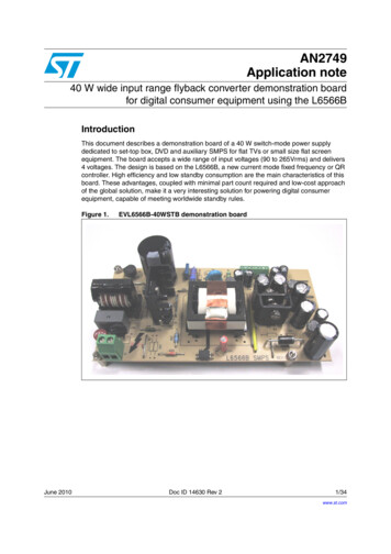
Main characteristics1AN2749Main characteristicsThe main characteristics of this SMPS are listed below: Input voltage: Vin: 90 - 264 Vrms f: 45-66 Hz Output voltages as given in Table 1Table 1.Output voltagesVoutIoutMAXIoutMINPMAXStabilityNotes1.8 V1.73 A0.20 A3.1 W 7%Dedicated to digital circuitry andto 1.2 V local post regulators3.3 V0.5 A0.03 A1.65 W 5%Dedicated to analog peripheralsand 2.5 V regulators5V2.4 A0.3 A12 W 10%Dedicated to HDD/DVD and 5 Vcircuitry12 V1.9 Avg2.9 Apk 8%Dedicated to HDD/DVD, SCARTand LNBP21 for satellite STB.Average load is 1.9 A, 2.9 A isdedicated to HDD/DVD spin-up0.05 A34.8 WPOUT (W) 40 W Avg / 51 W pk4/34 Standby: better than 800 mW at 230 Vin Short-circuit protection: on all outputs, with auto-restart at short removal PCB type and size: single-side 70 µm (2-Oz), CEM-1, 150 x 75 mm Safety: accordance with EN60065, creepage and clearance minimum distance 6.4 mm EMI: accordance with EN50022-Class BDoc ID 14630 Rev 2
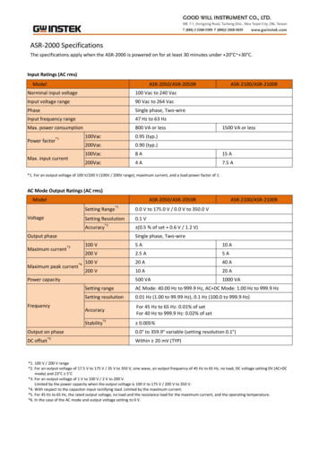
& X) 9& 10.'6 - 1 ; & 1& .5 17& 5 6 5 )86( S& : * ) 5 7 26&669)) &B2.%& %4 .5 1 1& . 5 .// ' 5 . 5 . 5 1 & 5 677 ' 1 55 & X 9& B& &20395() &'02'( 6&a5 / %',6&6)02'9FF*'*1' 96 98 ' / 5 %& %4 . 55 5 5 . .5 .5 5 0 5 . 5 & 1 95 5 5 673 1. )34 5 6 S)677 / 8' 5 . :5 0 & .5 .5 8 6) 5 1 & 65: /(& ( 7 %& %4 5 ) aDoc ID 14630 Rev 2 . X 9& %& % . 5 76 ,/78 . 1& . 5 // ' 700% 7 5 . . 5 5 5 1& . . .5 5 15 ' 5 55 X / X & & 1 . 4 X) 9& X) 95 1 ' X) 9/ & & X / X) 9& / X X) 9 X) 9&& 6736 / &)3' 6736 / '5 6 6 6736 )3 5 1 ' 5 & . 5 . 5 . 5 1& & 1 1& X) 9& 1& 9# X) 9& 9# X) 9& 9# X) 9& 9# 037 - Figure 2. 9DFAN2749Main characteristicsElectrical diagram!- V 5/34
Circuit description2AN2749Circuit descriptionThe topology of this converter is the classical flyback, working in continuous anddiscontinuous conduction mode with fixed frequency, capable of achieving the best trade-offbetween the peak-to-rms current ratio and output capacitor size. The nominal switchingfrequency, 62 kHz, has been chosen to arrive at a compromise between the transformersize and the harmonics of the switching frequency, optimizing the input filter size and itscost. The input EMI filter is a classical Pi-filter, 1-cell for differential mode noise. An NTC(R1) limits the inrush current produced by the capacitor charging at plug-in. The MOSFET isa standard and inexpensive 600 V-2 Ω max, TO-220FP, needing just a small heat sink. Thetransformer is a layer type, using a standard ferrite type EER28L. It has been designedaccording to the EN60065 and it is manufactured by TDK. The reflected voltage is 70 V,providing enough room for the leakage inductance voltage spike with still margin forreliability of the MOSFET. The network D7, R7, C21 clamps the peak of the leakageinductance voltage spike.The output rectifiers have been selected according to the maximum reverse voltage,forward-voltage drop and power dissipation. The rectifiers for 5 V and 12 V outputs areSchottky, low forward voltage drop type, hence dissipating less power with respect tostandard types. They are housed in TO-220 package. A small heat sink for both devices isrequired, as indicated in the bill of material (BOM). The other two output rectifiers areSchottky too but with a smaller package. The snubber R2 and C7 damps the oscillationproduced by the diode D2 at MOSFET turn-on. A small LC filter has been added on alloutputs in order to filter the high frequency ripple without increasing the output capacitorsand a capacitor (100 nF) has been placed on each output, to limit the spike amplitude.The output voltage regulation is performed by secondary feedback sensing the 12 V, 5 Vand 3.3 V outputs, while for 1.8 V output the regulation is achieved by the transformercoupling. The feedback network uses a TS2431 as error amplifier which drives anoptocoupler SFH617A-4, insuring the required insulation between primary and secondary.The opto-transistor modulates directly the voltage on COMP pin of the L6566B.The controller, the new L6566B, is an extremely versatile current mode primary controllerembedding all functions needed to get very high performance power supplies. It alsointegrates all protections needed by a power supply offering a very high degree of flexibilityto the designer.Furthermore the L6566B has a soft-start (pin#14), disable (pin#8) and 5 V reference voltageVREF (pin#10) available.Startup sequenceThe L6566B pin #1 (HV) is directly connected to the DC bulk voltage and at startup, aninternal high voltage current source charges C19 and C100 until the L6566B turn-on voltagethreshold is reached, then the high voltage current source is automatically switched off. Asthe L6566B starts switching it is initially supplied by the VCC capacitor, and then thetransformer auxiliary winding provides the voltage to power the IC. Because the L6566Bintegrated HV startup circuit is turned off, it is not dissipative during normal operation andhas a significant role to reduce the power consumption when the power supply operates atlight load. This contributes significantly to meet worldwide standby standards currentlyrequired.6/34Doc ID 14630 Rev 2
AN2749Circuit descriptionBrownout protectionBrownout protection prevents the circuit from working with abnormal mains levels. It can beeasily achieved using pin #16 (AC OK) of the L6566B. The divider R5, R6, R46, R12 andR13 is connected to the input DC bus and it is dedicated to sense the rectified input voltagepeak value and feed it into the L6566B AC OK pin. An internal comparator then enables theIC operations if the mains level is correct, within the nominal limits. If the input voltage isbelow 85Vac, the startup of the circuit is inhibited, while the turnoff voltage has been set atthe voltage reached by the bulk capacitor after the hold-up time. The internal comparatorhas in fact a current hysteresis allowing to set independently the L6566B turn-on and turnoffvoltage.L6566B current mode control and voltage feed-forward functionR18 and R19 sense the MOSFET current and the signal is fed into pin #7 (CS), connectedto the PWM comparator. This signal is thus compared with the COMP (pin #9) signal, whichis coming from the optocoupler.The maximum power that the converter can deliver is set by a comparator limiting the peakof the primary current, comparing the CS and an internal threshold (VCSX). If the currentsignal exceeds the threshold, the comparator limits the MOSFET duty cycle, hence theoutput power is also limited.Because the maximum transferable power depends on both the primary peak current andthe input voltage, in order to keep almost constant the overload set point that would changeaccording to flyback input voltage, the L6566B implements a voltage feed-forward functionvia a dedicated pin. Hence, VCSX is modulated by the voltage on pin #15 (VFF) sensing thebulk voltage by a resistor divider. A higher voltage causes a smaller VCS, MAX so that themaximum power can be kept almost constant at any input voltage.The resistor R27 connected between pin #7 (CS) and pin #12 (MODE/SC) provides thecorrect slope compensation to the current signal, required for the correct loop stability.L6566B short-circuit protectionIn case of short-circuit, an internal comparator senses the COMP pin after the soft-starttime. In that condition the COMP pin goes high, activating an internal current source thatrestarts charging the soft-start capacitor from the initial 2 V level. If the voltage on this pinreaches 5 V, the L6566B stops the operation and enters in "hiccup mode". The L6566Brestarts with a startup sequence when the Vcc voltage drops below the Vcc restart level (5V). Because of the long time needed by the Vcc capacitor to drop to 5 V, this results in anincrease of the duration of the no-load operation, thus decreasing the power dissipation andthe stress of the power components. This sequence is repeated until the short is removed,after that the normal operation of the converter is automatically resumed.Another comparator having its threshold at 1.5 V dedicated to protecting the circuit in caseof transformer saturation or secondary diodes short is provided too. If the voltage on the CSpin (#7) exceeds this threshold two consecutive times, the IC immediately shuts down andlatches off. This is intended to prevent spurious activation of the protection in case oftemporary disturbances, for example during the immunity tests. Even in this case the ICoperation is resumed as soon as the Vcc voltage drops below 5 V. In this way a hiccup modeoperation is still obtained, avoiding consequent failures due to overheating of the powercomponents . The sequence described here effectively protects the circuit if during the shortoperation the power supply delivers a significant high power at the output. Sometimes, inmulti-output SMPS in case of short on a low voltage output and especially when the powersupply is not delivering the full load, the power delivered to the shorted output could beDoc ID 14630 Rev 27/34
Circuit descriptionAN2749lower than the total maximum deliverable output power of the power supply. In that case thesituation would be critical because the power supply is delivering a high output current thatcould overheat the secondary side components, but the reduced power at primary sidewould not be able to trigger the overload protection at primary side. Therefore, an outputvoltage sensing on the lower voltage is implemented. Thus, in case a low voltage output isshorted, the abnormal lower value of that output is detected and the COMP pin is tied toGND by Q2 and Q3, pushing the circuit to work in hiccup mode.Overvoltage protectionThe pin #11 (ZCD) is connected to the auxiliary winding by a resistor divider. It implementsthe OVP against feedback network failures. When the ZCD pin voltage exceeds 5 V, the ICis shut down. This protection can be set as latch or auto-restart by the user with noadditional components. On the board it is set as latched. Therefore the operations can beresumed after a mains recycling.Standby power saving and light-load frequency foldback functionThe L6566B implements a current mode control, thus it monitors the output power by pinCOMP, which level is proportional to the load. Thus, when the voltage on pin COMP fallsbelow an internal threshold, the controller is disabled and its consumption reduced; Normaloperation restarts as soon as the COMP voltage rises again. In this way a low consumptionburst mode operation is obtained.The burst mode feature is dedicated to reduce the no load consumption but another targetof this application is achieving a high converter efficiency even at light load, when normally itis quite low. To improve the efficiency at this load condition a reduction of the switchingfrequency is needed, in order to save AC and transition losses of the power section. Asimple circuit realizing a frequency foldback, connected to the L6566B oscillator (pin #13 OSC) is implemented on the board. This solution allows improving light-load efficiencyrequiring just three external components.Frequency jitteringTo improve the EMI behavior of the application and make it quieter thus minimizing the EMIfilter, the L6566B is provided with a dedicated pin, FMOD (#6), allowing the user thepossibility to modulate the oscillator frequency in case the device is set for working in fixedfrequency mode. The FMOD pin (#6) gives the possibility to select both the modulationfrequency and the modulation depth. On the board, the capacitor C36 connected from thispin to GND is alternately charged and discharged by internal current sources. As a result,the voltage on the pin is a symmetrical triangular waveform with the frequency related to itsvalue. By connecting a resistor (R31) from this pin to pin OSC (#13) it is possible tomodulate the current sourced by the OSC pin and then the switching frequency. In thisboard a 400 Hz modulating frequency and 5 kHz of frequency deviation have been set.The modulation reduces the peak value of EMI emissions by means of a spread-spectrumaction. Please refer to Chapter 4: Conducted noise measurements on page 23 for therelevant measurements and comparison of the circuit working with or without the frequencyjittering function.8/34Doc ID 14630 Rev 2
AN2749Functional checking3Functional checking3.1Full-load operationThe following waveforms during normal operation at full load at different input voltages areshown for user reference:Figure 3.EVL6566B-40WSTB waveforms at115 Vac-60 Hz - full loadCH1: drain voltageCH2: L6566B pin#7 (CS)Figure 4.EVL6566B-40WSTB waveforms at230 Vac-50 Hz - full loadCH1: drain voltageCH2: L6566B pin#7 (CS)Figure 3 shows the drain voltage and current waveforms at 115 Vac while in Figure 4 thewaveforms are taken at 230 Vac. From the drain waveform it is possible to note that thetransformer is working in continuous mode. This operating mode has been chosen in orderto optimize the output filter capacitors and the peak-to-rms ratio of the current flowing in thetransformer windings. The measured switching frequency is 61 kHz. In Figure 5, the drainvoltage peak at full load and maximum input mains voltage has been measured. Themaximum voltage peak in this condition is 530 V, ensuring a reliable operation of theMOSFET with good margin against its maximum BVDSS.Doc ID 14630 Rev 29/34
Functional checkingFigure 5.AN2749EVL6566B-40WSTB waveforms at 265 V-50 Hz - full loadCH1: VdrainCH2: L6566B IsenThe following table shows the output voltage measurements and the overall efficiency of theconverter measured at nominal input mains voltages. All output voltages have beenmeasured on the output connector of the board.Table 2.EVL6566B-STB-40W efficiency measurement at full loadVin 115 Vac-60 HzVin 230 Vac-50 HzVoltage [V]Current [A]DeviationVoltage [V]Current .91%3.330.50.91%Pout [W] 39.10Pout [W] 38.9Pin [W] 50.6Pin [W] 48.95Efficiency 77.26 %Efficiency 79.47 %In Table 2 it is possible to note that all voltages are within the tolerance given in thespecification. The efficiency measured is very good for this kind of SMPS, thanks to theabsence of post regulators.In the followingTable 3 the output voltages are measured during the spin-up of the HDD orthe DVD, meaning a temporary increasing of the 12 V output current supplying the motor.The other output voltage loads are unchanged.10/34Doc ID 14630 Rev 2
AN2749Functional checkingTable 3.EVL6566B-STB-40W efficiency measurement at HDD spin-upVin 115 Vac-60 HzVin 230 Vac-50 HzVoltage [V]Current [A]DeviationVoltage [V]Current .52%3.350.51.52%Pout [W] 50.35Pout [W] 50.17Pin [W] 66.4Pin [W] 62.94Efficiency 75.83 %Efficiency 79.71 %As observable in this table, the output voltages are still within the given tolerance. Theheavier load does not affect efficiency. Please note that the total output power of Table 3 isthe so-called "electrical power", not the "thermal power". Therefore, the circuit has beendesigned to deliver the "electrical power" for a short time only - typically the HDD spin-uphas duration of 1 second - but it cannot be delivered significantly longer because, from thethermal point of view, the circuit can manage with the required reliability the full load only.3.2Reduced load operation, without the HDDThis reference board has been designed for powering digital equipment including a harddisk drive or a DVD but it can be used even for powering a set-top box or any other digitalequipment without the hard disk drive. A typical example could be an auxiliary SMPS of alarge screen flat-TV. The measurements shown in Table 4 provide for the output voltage andefficiency measurements in a load condition typical of a satellite set-top box.The 12 V and 5 V output currents have been reduced with respect to the previousmeasurements. As visible the output voltages are within the tolerances and the efficiency isat the same level of the previous test results.Table 4.Output voltage measurement at reduced load, without HDDVin 115 Vac-60 HzVin 230 Vac-50 out [W] 26.91Pout [W] 26.96Pin [W] 34.5Pin [W] 33.9Efficiency 78.01%Efficiency 79.52%Doc ID 14630 Rev 211/34
Functional checking3.3AN2749Minimum load operationEven at minimum load the power supply is still capable of regulating the output voltageswithin the specification tolerances, as indicated by the measurements in Table 5. Theefficiency is still high.Table 5.Output voltage measurement at reduced load, without HDDVin 115 Vac-60 HzVin 230 Vac-50 HzVoltage [V]Current [A]DeviationVoltage [V]Current 033.03%3.400.033.03%Pout [W] 2.52Pout [W] 2.53Pin [W] 3.43Pin [W] 3.69Efficiency 73.57 %Efficiency 68.47%Future new regulations and voluntary agreements for consumer and information technologyequipment require that power supplies and adapters have high efficiency not only at nominalor maximum load but also at minimum and light load. In these conditions most of the timegood efficiency is a difficult task to achieve, as it increases the complexity of control. By justadding a few external components, the oscillator structure of the L6566B can very easilyimplement a frequency foldback. Thus, the frequency reduction minimizes the switchinglosses, improving the power supply efficiency when it is working with an input power in therange of 1 to 30 W.The L6566B switching frequency is set by the current flowing in a resistor connectedbetween the OSC pin and ground (R15). During light-load operation the COMP (pin#9) leveldecreases and Q4 injects into R15 and OSC (pin #13) a current inversely proportional to theCOMP voltage. Because the voltage on pin OSC is constant (1 V), increasing Q4 currentprovides for the decrease of the current supplied by the pin and, as a consequence, theoscillator frequency. Thus, a frequency reduction proportional to the output load is easilyobtained.Figure 6 and 7 show the waveforms at different input power consumption. It can be notedthat the switching frequency is lower than the value measured at full load and decreasesproportionally to the COMP pin level.12/34Doc ID 14630 Rev 2
AN2749Figure 6.Functional checkingEVL6566B-40WSTB waveforms at230 V - Pin 30 WCH1: VdrainCH2: L6566B VGateCH3: L6566B VCompFigure 7.EVL6566B-40WSTB waveforms at230 V - Pin 4 WCH1: VdrainCH2: L6566B VGateCH3: L6566B VCompIf the load is further decreased, the L6566B works in burst mode. Once the COMP (pin#9)voltage drops below the internal threshold, the L6566B stops the gate driver operationdecreasing the internal circuitry consumption to minimize C19 discharging. Once the compvoltage rises above the internal burst mode threshold the device restarts switching. InFigure 8 and 9 the burst-mode waveforms are shown. The pictures are taken at 265 Vbecause at no-load condition the auxiliary voltage powering the L6566B falls at input mainsincreasing. This very often causes the supply voltage Vcc of the control IC to drop below theUVLO threshold so that the operation becomes intermittent, which is undesired.Furthermore, this must be traded off against the need of generating a voltage not exceedingthe maximum allowed by the control IC at full load to avoid overstress to the internal Vcc pinclamping circuitry and consequent overheating of the controller.To overcome this problem, the device, besides reducing its own consumption during burstmode operation, also features a proprietary adaptive UVLO function. It consists of shiftingthe UVLO threshold downwards at light load, namely when the voltage at pin COMP fallsbelow a threshold VCOMPO internally fixed, so as to have a greater margin. To prevent anymalfunction during transients from minimum to maximum load the normal (higher) UVLOthreshold is re-established when the voltage at pin COMP exceeds VCOMPL and Vcc hasexceeded the normal UVLO threshold. The normal UVLO threshold ensures that at full loadthe MOSFET is driven with a proper gate-to-source voltage. As visible in Figure 9 the Vcc ismeasured showing that there is a good margin with respect to the maximum turnoffthreshold (8 V maximum) of the L6566B.Doc ID 14630 Rev 213/34
Functional checkingFigure 8.AN2749EVL6566B-40WSTB waveforms at265 Vac - no loadFigure 9.EVL6566B-40WSTB waveforms at265 Vac - no load (detail)CH1: VdrainCH2: L6566B VCCCH3: L6566B VCompCH1: VdrainCH2: L6566B VCCCH3: L6566B VCompIn Table 6 the standby consumption is measured at both input mains voltages. Even in thisload condition the circuit is able to regulate the output voltages within the required tolerance.The input power is also measured. While delivering the standby load (5 V at 50 mA, 1.8 V,3.3 V and 12 V at 0 mA), the input power consumption is lower than 800 mW at bothnominal input voltage ranges.Table 6.Measurements during standby operationVin 115 Vac-60 HzVin 230 Vac-50 HzVoltage [V]Current [A]DeviationVoltage [V]Current .24%Pout [W] 0.24Pout [W] 0.24Pin [W] 0.648Pin [W] 0.798Efficiency 37.27%Efficiency 30.51%In Figure 10, the input power consumption over the input voltage range is shown. As visiblethere is just a small increase of the input power when the circuit is working close to themaximum input voltage.14/34Doc ID 14630 Rev 2
AN2749Functional checkingFigure 10. Input power vs. mains voltage during standbyThe diagram in the following Figure 11 represents the input power consumption as afunction of the 5 V output current. All other output voltages have no load as in the previousmeasurements. It is clearly visible that by decreasing the output current, the input power at230 Vac still decreases, keeping good efficiency of the circuit.Figure 11. Pin at 230 Vac vs. Iout 5
40 W wide input range flyback converter demonstration board for digital consumer equipment using the L6566B Introduction This document describes a demonstration board of a 40 W switch-mode power supply dedicated to set-top box, DVD and auxilia