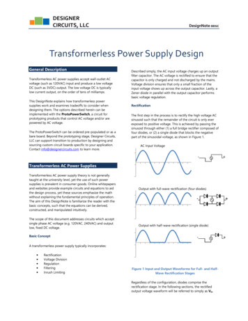
Transcription
Application ReportSLOA284 – January 2020Designing Bipolar High Voltage SEPIC Supply forUltrasound Smart ProbeElisa Granata, Abhishek Vishwa, Jun ShenABSTRACTMedical imaging, specifically ultrasound, is undergoing a significant transformation. A smart probeultrasound scanner is a handheld device that visualizes internal organs of the human body and their sizeusing advanced technology. The high degree of integration in front-and back-end units within a handhelddevice brings the designers face-to-face with challenges like power dissipation, thermal performance, sizeconstraints and noise immunity. This application note provides a solution to efficiently power ultrasoundtransmitters. This design generates bipolar programmable high voltage (HV) up to 80 V from a very lowvoltage source. It can deliver continuous average power of 2-W on each rail. A Single-Ended Primaryinductor Converter (SEPIC) topology with uncoupled inductors is preferred over transformer based flybackconverter in order to accomplish the critical height requirement ( 5 mm). It features symmetric rails ( 1%)and load regulation of 2%. It can be synchronized to an external clock to help filter out beat frequencies.This application report also provides a solution to generate programmable output voltage of up to 100 Vby the introduction of an intermediate boost stage.12345678ContentsIntroduction . 2Design of high voltage circuit using SEPIC topology . 4Test Results . 7Possible Variants of the Design . 11Layout Guidelines . 12Clock Synchronization . 13Summary . 14References . 14List of Figures1(left) Generic Smart Probe; (right) System Block Diagram of Smart Probe Ultrasound Scanner . 22Power Supply and TX RX AFE Boards3SEPIC Topology Scheme45678910111213141516. 3. 4Schematic of the High Voltage Circuit Design for Smart Probe . 5Power Supply Board Highlighting the HV Section . 5Efficiency Curve of SEPIC HV Power Supply . 7Load Symmetry of SEPIC Showing Accuracy of Less Than 1% and Load Regulation Less Than 2% . 7Output Ripple of Negative Rail Before Power Filter . 8Output Ripple of Negative Rail After Power Filter . 8Output Ripple of Positive Rail Before Power Filter . 8Output Ripple of Positive Rail After Power Filter . 8Load Transient Response of Positive and Negative Output Rail With Symmetrical Loads (25 mA) . 9Load Transient Response of Positive and Negative Output Rail With Symmetrical Loads (1A) . 9FFT of the Received Data Using Bench Power Supply, Showing SNR of 55.297 dB . 911 FFT of the Received Data Using SEPIC Power Supply, Showing SNR of 55.264 dB . 10Thermal Performance of High Voltage Section . 10SLOA284 – January 2020Submit Documentation FeedbackDesigning Bipolar High Voltage SEPIC Supply for Ultrasound Smart ProbeCopyright 2020, Texas Instruments Incorporated1
Introductionwww.ti.com17Implementation of Programmable Output . 1118Linearity of Output Voltage vs Control Voltage (VDAC)19Case of 1S Battery . 1220Case of 100 V . 1221Hot Loop in SEPIC Configuration . 1222Layout Section of HV . 1323Section of the Schematic of HV Supply Updated After Implementation of SYNC Functionality . 1324Synchronization at No Load With 50% Duty Cycle Clock25Synchronization at Full Load With 50% Duty Cycle Clock . 13.1113List of Tables1Design Specifications of High Voltage Power Supply in Smart Probe Ultrasound Scanner . 32Pros and Cons of Flyback and SEPIC Topology . 43Design Equations and Selected Components.6TrademarksWi-Fi is a registered trademark of Wi-Fi Alliance.All other trademarks are the property of their respective owners.1IntroductionUltrasound imaging is widely used technique for diagnostic purpose. In addition to high-performance cartbased ultrasound systems, it is now possible to use a handheld device (smart probe) to accomplish highquality ultrasound imaging. These smart probes leverage the power and resources of a mobile/tablet toprocess and display ultrasound images. A typical use case for these systems is to bring modern medicalimaging technology to remote places, making the diagnostics faster. This small equipment is typicallypowered by battery (1S/2S), or from USB source. The data can be transferred over USB or Wi-Fi .Figure 1 (left) shows a generic picture of such smart probe ultrasound scanner depicting a probeconnected to a mobile device. Figure 1 (right) shows the system level block diagram of the smart probe,which includes transmit (TX) and receive (RX) analog front end (AFEs) for transmitting and receivingultrasonic pulses and a FPGA to perform beam-forming. The whole setup is powered through the powersupply board, consisting of DC-DC converters to generate point of load voltages, HV circuit for TX andUSB controller for data and power management. This whole assembly of the analog front-end and powersupply module is shown in Figure 2, where the different sections are highlighted in red.PowerModuleHigh Voltage CircuitLow Voltage (PoL) CircuitTo DisplayToTransducer128ChannelsTransmitter4 x PGA (XC7A100T2CSGS24C)For digitalbeamformingUSBFX3USBType CPowerInputTIDA-010057Power Supply BoardTX RX BoardPower Supply BoardRx Tx BoardFigure 1. (left) Generic Smart Probe; (right) System Block Diagram of Smart Probe Ultrasound Scanner2Designing Bipolar High Voltage SEPIC Supply for Ultrasound Smart ProbeCopyright 2020, Texas Instruments IncorporatedSLOA284 – January 2020Submit Documentation Feedback
Introductionwww.ti.comFigure 2. Power Supply and TX RX AFE BoardsThis application report focuses on the generation of compact, transformer less high-voltage supply forpowering an ultrasound transmitter. This design generates programmable bipolar supply up to 80V, froma very low input voltage (typically 5 V) in a single stage. Key constraints of size and height are met byusing transformer-less SEPIC architecture. High efficiency of SEPIC architecture ensures low thermalfootprint. This design also achieves 2% load regulation, fast transient response, and very low noise. Thesolution can be synchronized to an external clock in order to enable filtering of beat frequencies.Table 1 below summarizes the design specifications of the high voltage circuit in the smart probeultrasound scanner.Table 1. Design Specifications of High Voltage Power Supply in Smart Probe Ultrasound ScannerCharacteristicsSpecifications Option-1: From USB power (4.25V to 5.5V DC) Option-2: From 1S/2S Li-Ion battery (3.6 V to 8.4 DC)Input voltage rangeOutput voltageBipolar (from 10 V to 80 V @ 25 mA and -10 V to -80 V @ 25 mA),symmetrical loadsPeak Efficiency75%Switching frequency250 kHzSize (length x width)15 mm x 45 mm (single layer)Height 5 mmOutput voltage regulation 2%Voltage symmetry with equal load on both rails 1%Output ripple0.1% of the output voltageSynchronization to external clock frequency1.1YesKey Design ChallengesThe quality of the final ultrasound image is directly dependent on the quality of the power supply, since thenoise from the supply can distort the image. The key design challenges are as follows: Dual rail HV ( 80 V @ 25 mA) generation from USB supply with single stage implementation andtransformer-less approach to achieve height 5 mm with HV Rail symmetry 1 % and load regulationwithin 2% Efficient layout and placement to achieve high signal to noise ratio (SNR) with noise floor below -90dBand data integrity, by minimizing conducted and radiated emissions Overall system efficiency 80% and thermal performance (temperature rise 15 C above ambient)SLOA284 – January 2020Submit Documentation FeedbackDesigning Bipolar High Voltage SEPIC Supply for Ultrasound Smart ProbeCopyright 2020, Texas Instruments Incorporated3
Introduction1.2www.ti.comPotential Topologies for Generating High Voltage SupplyConsidering the voltage requirements (up to 80 V, and 100 V in some cases) ,low power levels(approximately 2 W per rail) and small size of the solution, the most optimum power supply topologies areBoost/Cuk, Flyback and SEPIC. Since negative rail is required Flyback and SEPIC are better choices, dueto ease of implementation. A brief description and comparison of both topologies is provided below.SEPIC: SEPIC is a flexible topology that can function as step-up and step-down voltage regulator, itfeatures minimal active components, a simple controller, and clamped switching waveforms to minimizeswitching noiseFlyback: Flyback converter is the most commonly used SMPS circuit for low output power applicationswhere the output voltage must be isolated from the input main supply. The flyback topology is essentiallythe buck-boost topology that is isolated by using a transformer as the storage inductor.In Table 2, a comparison between Flyback and SEPIC converter is shown:Table 2. Pros and Cons of Flyback and SEPIC TopologyProsConsFlyback High step-up ratio Lower diode stress Lower magnetic components count Low efficiency at light loadsCustom transformer (height increases)Snubber requiredHigher surge currentHigher FET stressSEPIC Off-the-shelf inductors (height decreases) High efficiency at light loads Reduced switching losses (no leakage inductance oftransformer) Lower FET stress Smaller step-up ratio Higher diode stress Higher magnetic components countConsidering the challenges discussed in Section 1.1, Flyback topology is also suitable to generate bipolarhigh voltage supply. Nevertheless, the height of the Flyback transformer cannot accomplish an upper limitin the order of 5 mm (unless costly custom planar transformer is used in the design). This is the reason forselecting the SEPIC topology with off-the-shelf uncoupled inductors in this design.2Design of high voltage circuit using SEPIC topologyFigure 3 shows the generic schematic of the SEPIC topology. It uses three inductors: L1, L2 and L3. Thethree inductors can be wound on the same core since the same voltages are applied to them throughoutthe switching cycle and using a coupled inductor takes up less space on the PCB. However, they have tobe custom made and may not be small in height, hence this solution uses uncoupled inductors. Thecapacitor CS1 and CS2isolate the input from the output and provides protection against a shorted load.L1Cs1D1Vout Vin gure 3. SEPIC Topology Scheme4Designing Bipolar High Voltage SEPIC Supply for Ultrasound Smart ProbeCopyright 2020, Texas Instruments IncorporatedSLOA284 – January 2020Submit Documentation Feedback
Design of high voltage circuit using SEPIC topologywww.ti.comFor detailed information on SEPIC, see the Designing A SEPIC Converter and the LM3488/-Q1Automotive High-Efficiency Controller for Boost, SEPIC and Fly-Back DC-DC Converters. Thesedocuments refer to a coupled inductor approach, however the current solution adopts uncoupledinductors.2.1TI HV Supply Architecture Using SEPIC TopologyThis design implements a single stage architecture using only a single converter and a switch followed bytwo complementary output sections to generate the respective positive and negative HV rails. Custommade coupled inductors can benefit reduced energy losses due to leakage inductance, however, usinguncoupled inductors helps meet the height requirements and better components choice [1]. The feedbackis taken from positive output rail. Figure 4 shows the complete schematic of the design and Figure 5shows the physical picture of the board highlighting the HV section.Power FilterSync InputHV Voltage ShutdownProgrammable OutputFigure 4. Schematic of the High Voltage Circuit Design for Smart ProbeFigure 5. Power Supply Board Highlighting the HV SectionSLOA284 – January 2020Submit Documentation FeedbackDesigning Bipolar High Voltage SEPIC Supply for Ultrasound Smart ProbeCopyright 2020, Texas Instruments Incorporated5
Design of high voltage circuit using SEPIC topologywww.ti.comTable 3 explains the component selection, and equations for the SEPIC power converter using LM3488device.Table 3. Design Equations and Selected ComponentsParameterDuty cycleL1 (for minimum 40%current ripple )EquationsSelected ComponentsV OUTDVINVDV OUT94.15%VDVIN,MAX 2 u DL1 !R u FSW u POUT(1)o 70.1 (2)LM3488, which can reach a Duty cycle of100%.100 µH (23% of current ripple), Isat 1.2A,DCR 0.377 Ωwhere, R is %ripple of input of current (0.4)L2, L3 (for minimum40% current ripple) - L3,L4 in Figure 4L2 !1 D u VOUT 2R u FSW u POUTo 1020.8 1000 µH (41 % of current ripple) Isat 80 mA,(3) DCR 5.4Ωwhere, R is % ripple of input of current (0.4)MOSFET Q1 inFigure 4VSW(PEAK) VIN VOUT VD 86.28 86.28VTOFF 210 ns @ 250 kHz and D 94.14% ;VGS(TH) VINCSD19538Q3A VDS,MAX 100 V;RDS, ON 58 mΩ VGS,TH 3.2V;TOFF 9 nsVCS VIN, MAX ;CS2, CS3 - C25, C35in Figure 4D2, D3 - D3, D6I OUT u D MAXû9 CS(4)VIN VOUT 85V - Schottky diode to minimize lossesESR dCOUT2, COUT3 C70,C232, C30, C31,C71, C233, C36 inFigure 42.2 µF ; VDC 50V9C S u FSWV ripple u 0.5I L1 PEAKCOUT tI L2STPS1150 ;VFORWARD 0.78 V ; VRRM 150 Vd 42 m(5)PEAK4 x 2.2 µF - VDC 100 VIOUT x DMAXt 2.355 PFVripple x 0.5 x FSW(6)Vripple 1% *VoutCIN - C22, C23, C24in Figure 4ICIN RMSû,/0.18 A2x 47 µf - 0.1 µF - VDC 10 V12(7)1 DMAXf RHPZfR2u VOUT1.31 kHz2 u Œ u '0 ; u / u1u ,2873.35 kHz2 u Œ u / u &6(8)Compensation(RC,CC1 and CC2)R40, C27, C177 inFigure 4fCRCfR219 Hz6(9)2 u Œ u I& u &RXW u 9RXW 2 uRc 4.70 kΩ - Cc1 0.1 µF - Cc2 0.1 µF'0 ;GCS u GMA u VREF u VINMIN u DMAXWhere, GCS1RSN, where RSN20 A / V1.9 k, and GMA800 PKR(10)CC1CC2642 u Œ u IF u 5FCout u ESRRC1.5 )(11)47.4 pF(12)Designing Bipolar High Voltage SEPIC Supply for Ultrasound Smart ProbeCopyright 2020, Texas Instruments IncorporatedSLOA284 – January 2020Submit Documentation Feedback
Test Resultswww.ti.comThe output of the SEPIC circuit is cascaded with a π filter followed by an emitter follower configuration(power filter) in order to minimize the AC ripple. The filter is built in order to provide an attenuation of24.44 dB (see Equation 13) of the AC ripple as shown in Figure 8 through Figure 11 in Section 3.2.1Gain2§§ f · ·1 f0 ¹ ¹ (13)where f0 is the cut-off frequency of the RC filter and f is switching frequency of the input.3Test ResultsThe circuit shown in Figure 4 is characterized for performance with 5V input supply and test results arepresented in the subsequent sub-sections.3.1Efficiency and Load RegulationFigure 6 and Figure 7 shows the efficiency and load regulation of the power supply with symmetrical loadson the positive and the negative rail. The load is varied from 0 to 25 mA on each rail. The peak efficiencyobserved is 75 % and worst case load regulation is 1.99 %. The positive and negative outputs aresymmetrical within 1% with respect to each other.80100708060Output Voltage (V)Efficiency (%)6050403040200Positive Rail ( 75 V)Negative Rail (-75 V)-20-4020-6010-80Hight Voltage Circuit with Power Filter0-10005101520Output Current (mA)25300D001Figure 6. Efficiency Curve of SEPIC HV Power SupplySLOA284 – January 2020Submit Documentation Feedback5101520Output Current (mA)2530D002Figure 7. Load Symmetry of SEPIC Showing Accuracy ofLess Than 1% and Load Regulation Less Than 2%Designing Bipolar High Voltage SEPIC Supply for Ultrasound Smart ProbeCopyright 2020, Texas Instruments Incorporated7
Test Results3.2www.ti.comOutput Ripple MeasurementFigure 8 and Figure 10 shows the output ripple of the high voltage circuit of both negative and positive railat full load, respectively. The ripple is measured at the output capacitor before the π filter, the peak to peakripple is close to 25 mV. Figure 9 and Figure 11 shows the ripple measured after the Power Filter, which issignificantly attenuated.8Figure 8. Output Ripple of Negative Rail Before PowerFilterFigure 9. Output Ripple of Negative Rail After PowerFilterFigure 10. Output Ripple of Positive Rail Before PowerFilterFigure 11. Output Ripple of Positive Rail After PowerFilterDesigning Bipolar High Voltage SEPIC Supply for Ultrasound Smart ProbeCopyright 2020, Texas Instruments IncorporatedSLOA284 – January 2020Submit Documentation Feedback
Test Resultswww.ti.com3.3Load Transient TestFigure 12 shows the load transient response of the power supply. The load of 25 mA per rail is appliedonto both positive and negative rail with a duty cycle 20% at pulse repetition frequency of 5 kHz, as shownin purple waveform. A drop of less than 50 mV is observed on both the rails. Moreover, the load transientresponse test is repeated in case the load of the power supply is 1 A per rail with a duty cycle of 1%, atpulse repetition frequency of 5 kHz. The result in Figure 13, shows a drop of less than 1 V per rail.Figure 12. Load Transient Response of Positive andNegative Output Rail With Symmetrical Loads (25 mA)3.4Figure 13. Load Transient Response of Positive andNegative Output Rail With Symmetrical Loads (1A)Noise MeasurementFigure 14 and Figure 15 show the FFT of the received data collected from TX RX setup consisting ofTX7332 as transmit device and AFE5832LP as receive device. Figure 14 shows the noise with idealbench supply and Figure 15 shows the noise with High Voltage supply generated by this design. The SNRin case of bench power supply and SEPIC based supply are 55.297 dB & 55.264 dB, respectively. Thisdemonstrates that the noise performance of this design is comparable with the bench power supply.Figure 14. FFT of the Received Data Using Bench Power Supply, Showing SNR of 55.297 dBSLOA284 – January 2020Submit Documentation FeedbackDesigning Bipolar High Voltage SEPIC Supply for Ultrasound Smart ProbeCopyright 2020, Texas Instruments Incorporated9
Test Resultswww.ti.comFigure 15. 11 FFT of the Received Data Using SEPIC Power Supply, Showing SNR of 55.264 dB3.5Thermal PerformanceFigure 16 shows a thermal image of the high voltage circuit, with symmetrical load of 25 mA on each railwith 20 % duty cycle at 5 kHz shown in Figure 12. The maximum temperature is 34.7 C, reached after 30minutes of powering on at ambient temperature of 20 C.Figure 16. Thermal Performance of High Voltage Section10Designing Bipolar High Voltage SEPIC Supply for Ultrasound Smart ProbeCopyright 2020, Texas Instruments IncorporatedSLOA284 – January 2020Submit Documentation Feedback
Possible Variants of the Designwww.ti.com4Possible Variants of the DesignThis section shows possible variations of this design.4.1Option 1: Programmable Output VoltageBased on the various ultrasound operating modes, the output of the high voltage circuit should beprogrammable. This can be implemented as shown in Figure 4 by replacing the diode D18 with oneresistor R3, joining the feedback resistors (shown in Figure 17). Output voltage can be varied through thecontrol voltage (VDAC). Resistors can be set using equations (2), (3), (4) where R1 and R2 are thefeedback resistors.VoutR1R3VrefVadjR2Figure 17. Implementation of Programmable OutputI R1.minR3R2V out,minV refR1V adj,max u R 1V out,maxV ref(14)R 1 u I R1,min(15)V ref u R 1 u R 3R 3 u V out,maxR 1 u V refR 3 u V ref(16)shows linear relationship between the programmed output voltage and the control voltage.9080Output Voltage (V)7060504030201000123DAC Voltage (V)45D003Figure 18. Linearity of Output Voltage vs Control Voltage (VDAC)The designer should take care of the saturation current rating of the secondary inductors to take care ofincreased output current at reduced output voltage. In SEPIC converter the current is provided mainlyfrom secondary inductors during off time. In this design, the secondary inductors are rated for 80 mA.SLOA284 – January 2020Submit Documentation FeedbackDesigning Bipolar High Voltage SEPIC Supply for Ultrasound Smart ProbeCopyright 2020, Texas Instruments Incorporated11
Possible Variants of the Design4.2www.ti.comOption 2: Support Input From 1S Li-Ion Battery1S Li-Ion battery has a typical operating voltage range of 3.0 V to 4.2 V. To generate an output voltage of /- 80V, the existing SEPIC needs a PWM controller that can achieve high duty cycle 95%. At thesevery high duty cycle there are practical limitations such as: parasitics which affect the turn-on and turn-offtime of the MOSFET, lower available time for energy transfer from primary to secondary side which limitthe achievable maximum output voltage. Hence an intermediate boost stage is required to be added, asshown in Figure 19.IntermediateVoltagei.e. 5 V3.6 V to 4.2 VSEPICPre-boost /- 80 VFigure 19. Case of 1S Battery4.3Option 3: Output Voltage Up to 100 VIn some cases ultrasound probes may require 100 V. The same limitations mentioned in option 2 areapplicable. To achieve this, an intermediate boost stage is needed to boost the input to a minimum of 12 Vto have a duty cycle of approximately 90%, as shown in Figure 20.IntermediateVoltagei.e. 12 V4.25 V to 5.5 VSEPICPre-boost /- 100 VFigure 20. Case of 100 V[Note: the components ratings should be taken care in both these cases. For instance, the MOSFET insecond case has to withstand about 113 V, and the coupling capacitor has to be rated for 20 V.5Layout GuidelinesLayout in SEPIC is very critical. While designing, the most important rule is to reduce the noise in the highcurrent switching loop, which is shown in Figure 21. The current flows from the input supply to the primaryinductor and through the MOSFET. To minimize induced EMF due to switching currents, it is desirable tokeep parasitic inductance of this loop as low as possible. Components (primary inductors, input electrolyticcapacitors, and FET) must be placed as close as possible to each other. In this layout, a single groundplane was used, and all the signals return onto this low impedance plane, as shown in Figure 22. In casethe HV circuit is placed in proximity to the transducer, shielding might be necessary to minimize effects ofradiated interference from HV section.CSL1D1VINVOUTCINQ1L2COUTFigure 21. Hot Loop in SEPIC Configuration12Designing Bipolar High Voltage SEPIC Supply for Ultrasound Smart ProbeCopyright 2020, Texas Instruments IncorporatedSLOA284 – January 2020Submit Documentation Feedback
Clock Synchronizationwww.ti.comFigure 22. Layout Section of HV6Clock SynchronizationThe schematic shown in Figure 4 can be synchronized to an external clock signal only if the duty cycle ofthe latter is larger than the duty cycle of the controller itself (larger than 93%). This design can besynchronized to an external clock with 50% Duty cycle by implementing the solution shown in Figure 23.Two diodes forming an OR-ing system are introduced. One diode is placed from the gate drive pin to thesync pin. The other one comes from the input clock signal. The resistor R36 and R39 are series SYNCresistor and discharge resistor, respectively. If DR pin is more positive than SYNC HV TX, then D1 willbe reverse-biased and the SYNC-PIN will be driven high from D2. If DR pin is less positive thanSYNC HV TX, then D2 will be reverse-biased and SYNC PIN will be driven High from D1. Test resultsare shown in Figure 24 andFigure 23. Section of the Schematic of HV Supply Updated After Implementation of SYNC FunctionalitySLOA284 – January 2020Submit Documentation FeedbackDesigning Bipolar High Voltage SEPIC Supply for Ultrasound Smart ProbeCopyright 2020, Texas Instruments Incorporated13
Summarywww.ti.comFigure 24. Synchronization at No Load With 50% DutyCycle Clock7Figure 25. Synchronization at Full Load With 50% DutyCycle ClockSummaryThe rapid evolution of ultrasound smart probes is changing the medical landscape and is helping providebetter healthcare in remote places. The advent of these handheld devices is coming with the bigchallenges of compact size, high noise immunity, efficiency and thermal performance. This design, by theselection of SEPIC topology over the traditional transformer-based flyback topology, helps in solving somekey- challenges for generating high voltage from low input voltage, in the desired size and height, whilemaintaining a high efficiency, low noise, good load regulation and symmetry. Based on the voltagerequirement of the ultrasound transducer and operating modes, the output of high voltage circuit supportsprogrammability.8References1. Texas Instruments: Benefits of a coupled-inductor SEPIC converter2. Texas Instruments: LM3488/-Q1 Automotive High-Efficiency Controller for Boost, SEPIC and Fly-BackDC-DC Converters Data Sheet3. Texas Instruments: Designing A SEPIC Converter14Designing Bipolar High Voltage SEPIC Supply for Ultrasound Smart ProbeCopyright 2020, Texas Instruments IncorporatedSLOA284 – January 2020Submit Documentation Feedback
IMPORTANT NOTICE AND DISCLAIMERTI PROVIDES TECHNICAL AND RELIABILITY DATA (INCLUDING DATA SHEETS), DESIGN RESOURCES (INCLUDING REFERENCEDESIGNS), APPLICATION OR OTHER DESIGN ADVICE, WEB TOOLS, SAFETY INFORMATION, AND OTHER RESOURCES “AS IS”AND WITH ALL FAULTS, AND DISCLAIMS ALL WARRANTIES, EXPRESS AND IMPLIED, INCLUDING WITHOUT LIMITATION ANYIMPLIED WARRANTIES OF MERCHANTABILITY, FITNESS FOR A PARTICULAR PURPOSE OR NON-INFRINGEMENT OF THIRDPARTY INTELLECTUAL PROPERTY RIGHTS.These resources are intended for skilled developers designing with TI products. You are solely responsible for (1) selecting the appropriateTI products for your application, (2) designing, validating and testing your application, and (3) ensuring your application meets applicablestandards, and any other safety, security, regulatory or other requirements.These resources are subject to change without notice. TI grants you permission to use these resources only for development of anapplication that uses the TI products described in the resource. Other reproduction and display of these resources is prohibited. No licenseis granted to any other TI intellectual property right or to any third party intellectual property right. TI disclaims responsibility for, and youwill fully indemnify TI and its representatives against, any claims, damages, costs, losses, and liabilities arising out of your use of theseresources.TI’s products are provided subject to TI’s Terms of Sale or other applicable terms available either on ti.com or provided in conjunction withsuch TI products. TI’s provision of these resources does not expand or otherwise alter TI’s applicable warranties or warranty disclaimers forTI products.TI objects to and rejects any additional or different terms you may have proposed. IMPORTANT NOTICEMailing Address: Texas Instruments, Post Office Box 655303, Dallas, Texas 75265Copyright 2022, Texas Instruments Incorporated
Designing Bipolar High Voltage SEPIC Supply for Ultrasound Smart Probe 1.2 Potential Topologies for Generating High Voltage Supply Considering the voltage requirements (up to 80 V, and 100 V in some cases) ,low power levels (approximately 2 W per rail) and small size of the solution, the most optimum power supply topologies are