Transcription
Intel MAX 10 FPGA DeviceOverviewSubscribeSend FeedbackM10-OVERVIEW 2017.12.15Latest document on the web: PDF HTML
ContentsContentsIntel MAX 10 FPGA Device Overview.3Key Advantages of Intel MAX 10 Devices. 3Summary of Intel MAX 10 Device Features . 4Intel MAX 10 Device Ordering Information.5Intel MAX 10 Device Feature Options. 6Intel MAX 10 Device Maximum Resources .6Intel MAX 10 Devices I/O Resources Per Package .7Intel MAX 10 Vertical Migration Support. 7Intel MAX 10 I/O Vertical Migration Support.8Intel MAX 10 ADC Vertical Migration Support. 8Logic Elements and Logic Array Blocks. 9Analog-to-Digital Converter. 9User Flash Memory. 10Embedded Multipliers and Digital Signal Processing Support. 10Embedded Memory Blocks. 11Clocking and PLL. 11FPGA General Purpose I/O. 12External Memory Interface. 12Configuration.13Power Management. 13Document Revision History for Intel MAX 10 FPGA Device Overview. 13Intel MAX 10 FPGA Device Overview2
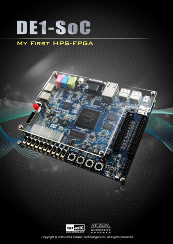
M10-OVERVIEW 2017.12.15Intel MAX 10 FPGA Device OverviewIntel MAX 10 devices are single-chip, non-volatile low-cost programmable logicdevices (PLDs) to integrate the optimal set of system components.The highlights of the Intel MAX 10 devices include: Internally stored dual configuration flash User flash memory Instant on support Integrated analog-to-digital converters (ADCs) Single-chip Nios II soft core processor supportIntel MAX 10 devices are the ideal solution for system management, I/O expansion,communication control planes, industrial, automotive, and consumer applications.Related LinksIntel MAX 10 FPGA Device DatasheetKey Advantages of Intel MAX 10 DevicesTable 1.Key Advantages of Intel MAX 10 DevicesAdvantageSupporting FeatureSimple and fast configurationSecure on-die flash memory enables device configuration in less than 10 msFlexibility and integration Low power Single device integrating PLD logic, RAM, flash memory, digital signalprocessing (DSP), ADC, phase-locked loop (PLL), and I/OsSmall packages available from 3 mm 3 mmSleep mode—significant standby power reduction and resumption in less than1 msLonger battery life—resumption from full power-off in less than 10 ms20-year-estimated life cycleBuilt on TSMC's 55 nm embedded flash process technologyHigh productivity design tools Intel Quartus Prime Lite edition (no cost license)Platform Designer (Standard) system integration toolDSP Builder for Intel FPGAsNios II Embedded Design Suite (EDS)Intel Corporation. All rights reserved. Intel, the Intel logo, Altera, Arria, Cyclone, Enpirion, MAX, Nios, Quartusand Stratix words and logos are trademarks of Intel Corporation or its subsidiaries in the U.S. and/or othercountries. Intel warrants performance of its FPGA and semiconductor products to current specifications inaccordance with Intel's standard warranty, but reserves the right to make changes to any products and servicesat any time without notice. Intel assumes no responsibility or liability arising out of the application or use of anyinformation, product, or service described herein except as expressly agreed to in writing by Intel. Intelcustomers are advised to obtain the latest version of device specifications before relying on any publishedinformation and before placing orders for products or services.*Other names and brands may be claimed as the property of others.ISO9001:2008Registered
Intel MAX 10 FPGA Device OverviewM10-OVERVIEW 2017.12.15Summary of Intel MAX 10 Device FeaturesTable 2.Summary of Features for Intel MAX 10 DevicesFeatureDescriptionTechnology55 nm TSMC Embedded Flash (Flash SRAM) process technologyPackaging Low cost, small form factor packages—support multiple packagingtechnologies and pin pitchesMultiple device densities with compatible package footprints for seamlessmigration between different device densitiesRoHS6-compliantCore architecture 4-input look-up table (LUT) and single register logic element (LE)LEs arranged in logic array block (LAB)Embedded RAM and user flash memoryClocks and PLLsEmbedded multiplier blocksGeneral purpose I/OsInternal memory blocks M9K—9 kilobits (Kb) memory blocksCascadable blocks to create RAM, dual port, and FIFO functionsUser flash memory (UFM) User accessible non-volatile storageHigh speed operating frequencyLarge memory sizeHigh data retentionMultiple interface optionEmbedded multiplier blocks One 18 18 or two 9 9 multiplier modesCascadable blocks enabling creation of filters, arithmetic functions, and imageprocessing pipelinesADC 12-bit successive approximation register (SAR) typeUp to 17 analog inputsCumulative speed up to 1 million samples per second ( MSPS)Integrated temperature sensing capabilityClock networks Global clocks supportHigh speed frequency in clock networkInternal oscillatorBuilt-in internal ring oscillatorPLLs Analog-basedLow jitterHigh precision clock synthesisClock delay compensationZero delay bufferingMultiple output tapsGeneral-purpose I/Os (GPIOs) Multiple I/O standards supportOn-chip termination (OCT)Up to 830 megabits per second (Mbps) LVDS receiver, 800 Mbps LVDStransmitter External memory interface (EMIF)(1)Supports up to 600 Mbps external memory interfaces:continued.(1)EMIF is only supported in selected Intel MAX 10 device density and package combinations.Refer to the External Memory Interface User Guide for more information.Intel MAX 10 FPGA Device Overview4
Intel MAX 10 FPGA Device OverviewM10-OVERVIEW 2017.12.15FeatureDescription DDR3, DDR3L, DDR2, LPDDR2 (on 10M16, 10M25, 10M40, and 10M50.)SRAM (Hardware support only)Note: For 600 Mbps performance, –6 device speed grade is required.Performance varies according to device grade (commercial, industrial, orautomotive) and device speed grade (–6 or –7). Refer to the Intel MAX10 FPGA Device Datasheet or External Memory Interface Spec Estimatorfor more details.Configuration Flexible power supply schemes Internal configurationJTAGAdvanced Encryption Standard (AES) 128-bit encryption and compressionoptionsFlash memory data retention of 20 years at 85 C Single- and dual-supply device optionsDynamically controlled input buffer power downSleep mode for dynamic power reductionIntel MAX 10 Device Ordering InformationFigure 1.Sample Ordering Code and Available Options for Intel MAX 10 DevicesMember Code02040816254050:::::::Package Type2K logic elements4K logic elements8K logic elements16K logic elements25K logic elements40K logic elements50K logic elementsFamily Signature10M : Intel MAX 10VEMUF:::::Wafer-Level Chip Scale (WLCSP)Plastic Enhanced Quad Flat Pack (EQFP)Micro FineLine BGA (MBGA)Ultra FineLine BGA (UBGA)FineLine BGA (FBGA)Operating Temperature10M 16DAU 484I7 GFPGA FabricSpeed GradeFeature OptionsSC : Single supply - compact featuresSA : Single supply - analog and flash featureswith RSU optionDC : Dual supply - compact featuresDF : Dual supply - flash features with RSU optionDA : Dual supply - analog and flash featureswith RSU option6 (fastest)78CIA: Commercial (TJ 0 C to 85 C): Industrial (TJ - 40 C to 100 C): Automotive (TJ - 40 C to 125 C)Optional SuffixIndicates specific deviceoptions or shipment methodG : RoHS6ES : Engineering sampleP : Leaded packagePackage CodeWLCSP Package Type36 : 36 pins, 3 mm x 3 mm81 : 81 pins, 4 mm x 4 mmUBGA Package Type169 : 169 pins, 11 mm x 11 mm324 : 324 pins, 15 mm x 15 mmEQFP Package TypeFBGA Package Type144 : 144 pins, 22 mm x 22 mm 256 : 256 pins, 17 mm x 17 mm484 : 484 pins, 23 mm x 23 mmMBGA Package Type672 : 672 pins, 27 mm x 27 mm153 : 153 pins, 8 mm x 8 mmNote:The –I6 and –A6 speed grades of the Intel MAX 10 FPGA devices are not available bydefault in the Intel Quartus Prime software. Contact your local Intel salesrepresentatives for support.Related LinksIntel FPGA Product SelectorProvides the latest information about Intel FPGAs.Intel MAX 10 FPGA Device Overview5
Intel MAX 10 FPGA Device OverviewM10-OVERVIEW 2017.12.15Intel MAX 10 Device Feature OptionsTable 3.Feature Options for Intel MAX 10 DevicesOptionFeatureCompactDevices with core architecture featuring single configuration image with self-configuration capabilityFlashDevices with core architecture featuring: Dual configuration image with self-configuration capability Remote system upgrade capability Memory initializationAnalogDevices with core architecture featuring: Dual configuration image with self-configuration capability Remote system upgrade capability Memory initialization Integrated ADCIntel MAX 10 Device Maximum ResourcesTable 4.Maximum Resource Counts for Intel MAX 10 d Receiver114114116151171241241Internal Configuration Image1222222ADC—111222Logic Elements (LE) (K)M9K Memory (Kb)User Flash Memory (Kb)(2)18 18 MultiplierPLLGPIOLVDS(2)The maximum possible value including user flash memory and configuration flash memory. Formore information, refer to Intel MAX 10 User Flash Memory User Guide.Intel MAX 10 FPGA Device Overview6
Intel MAX 10 FPGA Device OverviewM10-OVERVIEW 2017.12.15Intel MAX 10 Devices I/O Resources Per PackageTable 5.Package Plan for Intel MAX 10 Single Power Supply DevicesDevicePackageTypeM153153-pin MBGAU169169-pin UBGAU324324-pin UBGAE144144-pin EQFPSize8 mm 8 mm11 mm 11 mm15 mm 15 mm22 mm 22 mmBall Pitch0.5 mm0.8 mm0.8 mm0.5 �10110M50———101Table 6.Package Plan for Intel MAX 10 Dual Power Supply in WLCSP 81-pin WLCSP 324-pin UBGA 256-pin FBGA 484-pin FBGA 672-pin FBGASize3 mm 3 mm 4 mm 4 mmBall Pitch15 mm 15mm17 mm 17mm23 mm 23mm27 mm 27mm0.4 mm0.4 mm0.8 mm1.0 mm1.0 mm1.0 ��178360500Related Links Intel MAX 10 General Purpose I/O User Guide Intel MAX 10 High-Speed LVDS I/O User GuideIntel MAX 10 Vertical Migration SupportVertical migration supports the migration of your design to other Intel MAX 10 devicesof different densities in the same package with similar I/O and ADC resources.Intel MAX 10 FPGA Device Overview7
Intel MAX 10 FPGA Device OverviewM10-OVERVIEW 2017.12.15Intel MAX 10 I/O Vertical Migration SupportFigure 2.Migration Capability Across Intel MAX 10 Devices The arrows indicate the migration paths. The devices included in each vertical migration path are shaded.Non-migratable devices are omitted. Some packages have several migration paths. Devices with lesserI/O resources in the same path have lighter shades. To achieve the full I/O migration across product lines in the same migration path, restrict I/Os usage tomatch the product line with the lowest I/O 67210M0210M0410M0810M1610M2510M4010M50Dual Power Supply DevicesNote:Single Power Supply DevicesTo verify the pin migration compatibility, use the Pin Migration View window in theIntel Quartus Prime software Pin Planner.Intel MAX 10 ADC Vertical Migration SupportFigure 3.ADC Vertical Migration Across Intel MAX 10 DevicesThe arrows indicate the ADC migration paths. The devices included in each vertical migration path are 0M0810M1610M2510M4010M50Dual ADC Device: Each ADC (ADC1 and ADC2) supports 1 dedicated analog input pin and 8 dual function pins.Single ADC Device: Single ADC that supports 1 dedicated analog input pin and 16 dual function pins.Single ADC Device: Single ADC that supports 1 dedicated analog input pin and 8 dual function pins.Intel MAX 10 FPGA Device Overview8F672
Intel MAX 10 FPGA Device OverviewM10-OVERVIEW 2017.12.15Table 7.Pin Migration Conditions for ADC MigrationSourceTargetSingle ADC deviceSingle ADC deviceDual ADC deviceDual ADC deviceSingle ADC deviceDual ADC deviceDual ADC deviceSingle ADC deviceMigratable PinsYou can migrate all ADC input pins One dedicated analog input pin.Eight dual function pins from the ADC1 block of thesource device to the ADC1 block of the target device.Logic Elements and Logic Array BlocksThe LAB consists of 16 logic elements (LE) and a LAB-wide control block. An LE is thesmallest unit of logic in the Intel MAX 10 device architecture. Each LE has four inputs,a four-input look-up table (LUT), a register, and output logic. The four-input LUT is afunction generator that can implement any function with four variables.Figure 4.Intel MAX 10 Device Family LEsRegister chain routingLAB-WideLAB-widefrom previous LE synchronous load synchronous clearLE carry-indata 1data 2data 3SynchronousLoad andClear LogicLook-Up Table CarryChain(LUT)data 4labclr1labclr2Chip-wide reset(DEV CLRn)Register feedbackLE Carry-Outlabclk1DRegister bypassProgrammable registerQENACLRNAsynchronousClear LogicRow, column, anddirect link routingRow, column, anddirect link routingLocal routingClock andClock EnableSelectRegister chain outputlabclk2labclkena1labclkena2Analog-to-Digital ConverterIntel MAX 10 devices feature up to two ADCs. You can use the ADCs to monitor manydifferent signals, including on-chip temperature.Table 8.ADC FeaturesFeature12-bit resolutionDescription Up to 1 MSPS sampling rateTranslates analog signal to digital data for information processing, computing,data transmission, and control systemsProvides a 12-bit digital representation of the observed analog signalMonitors single-ended external inputs with a cumulative sampling rate of 25kilosamples per second to 1 MSPS in normal modecontinued.Intel MAX 10 FPGA Device Overview9
Intel MAX 10 FPGA Device OverviewM10-OVERVIEW 2017.12.15FeatureDescriptionUp to 17 single-ended external inputsfor single ADC devicesOne dedicated analog and 16 dual function input pinsUp to 18 single-ended external inputsfor dual ADC devices On-chip temperature sensorMonitors external temperature data input with a sampling rate of up to 50kilosamples per secondOne dedicated analog and eight dual-function input pins in each ADC blockSimultaneous measurement capability for dual ADC devicesUser Flash MemoryThe user flash memory (UFM) block in Intel MAX 10 devices stores non-volatileinformation.UFM provides an ideal storage solution that you can access using Avalon MemoryMapped (Avalon-MM) slave interface protocol.Table 9.UFM FeaturesFeaturesCapacityEnduranceCounts to at least 10,000 program/erase cyclesData retention Operating frequencyMaximum 116 MHz for parallel interface and 7.25 MHz forserial interfaceData lengthStores data up to 32 bits length in parallel20 years at 85 ºC10 years at 100 ºCEmbedded Multipliers and Digital Signal Processing SupportIntel MAX 10 devices support up to 144 embedded multiplier blocks. Each blocksupports one individual 18 18-bit multiplier or two individual 9 9-bit multipliers.With the combination of on-chip resources and external interfaces in Intel MAX 10devices, you can build DSP systems with high performance, low system cost, and lowpower consumption.You can use the Intel MAX 10 device on its own or as a DSP device co-processor toimprove price-to-performance ratios of DSP systems.You can control the operation of the embedded multiplier blocks using the followingoptions: Parameterize the relevant IP cores with the Intel Quartus Prime parameter editor Infer the multipliers directly with VHDL or Verilog HDLSystem design features provided for Intel MAX 10 devices:Intel MAX 10 FPGA Device Overview10
Intel MAX 10 FPGA Device OverviewM10-OVERVIEW 2017.12.15 DSP IP cores:—Common DSP processing functions such as finite impulse response (FIR), fastFourier transform (FFT), and numerically controlled oscillator (NCO) functions—Suites of common video and image processing functions Complete reference designs for end-market applications DSP Builder for Intel FPGAs interface tool between the Intel Quartus Primesoftware and the MathWorks Simulink and MATLAB design environments DSP development kitsEmbedded Memory BlocksThe embedded memory structure consists of M9K memory blocks columns. Each M9Kmemory block of a Intel MAX 10 device provides 9 Kb of on-chip memory capable ofoperating at up to 284 MHz. The embedded memory structure consists of M9Kmemory blocks columns. Each M9K memory block of a Intel MAX 10 device provides9 Kb of on-chip memory. You can cascade the memory blocks to form wider or deeperlogic structures.You can configure the M9K memory blocks as RAM, FIFO buffers, or ROM.The Intel MAX 10 device memory blocks are optimized for applications such as highthroughput packet processing, embedded processor program, and embedded datastorage.Table 10.M9K Operation Modes and Port WidthsOperation ModesPort WidthsSingle port 1, 2, 4, 8, 9, 16, 18, 32, and 36Simple dual port 1, 2, 4, 8, 9, 16, 18, 32, and 36True dual port 1, 2, 4, 8, 9, 16, and 18Clocking and PLLIntel MAX 10 devices offer the following resources: global clock (GCLK) networks andphase-locked loops (PLLs) with a 116-MHz built-in oscillator.Intel MAX 10 devices support up to 20 global clock (GCLK) networks with operatingfrequency up to 450 MHz. The GCLK networks have high drive strength and low skew.The PLLs provide robust clock management and synthesis for device clockmanagement, external system clock management, and I/O interface clocking. Thehigh precision and low jitter PLLs offers the following features: Reduction in the number of oscillators required on the board Reduction in the device clock pins through multiple clock frequency synthesis froma single reference clock source Frequency synthesis On-chip clock de-skew Jitter attenuation Dynamic phase-shiftIntel MAX 10 FPGA Device Overview11
Intel MAX 10 FPGA Device OverviewM10-OVERVIEW 2017.12.15 Zero delay buffer Counter reconfiguration Bandwidth reconfiguration Programmable output duty cycle PLL cascading Reference clock switchover Driving of the ADC blockFPGA General Purpose I/OThe Intel MAX 10 I/O buffers support a range of programmable features.These features increase the flexibility of I/O utilization and provide an alternative toreduce the usage of external discrete components such as a pull-up resistor and a PCIclamp diode.External Memory InterfaceDual-supply Intel MAX 10 devices feature external memory interfaces solution thatuses the I/O elements on the right side of the devices together with the UniPHY IP.With this solution, you can create external memory interfaces to 16-bit SDRAMcomponents with error correction coding (ECC).Note:The external memory interface feature is available only for dual-supply Intel MAX 10devices.Table 11.External Memory Interface PerformanceExternal MemoryInterface(3)I/O StandardMaximum WidthMaximum Frequency (MHz)DDR3 SDRAMSSTL-1516 bit 8 bit ECC303DDR3L SDRAMSSTL-13516 bit 8 bit ECC303DDR2 SDRAMSSTL-1816 bit 8 bit ECC200LPDDR2 SDRAMHSUL-1216 bit without ECC200(4)Related LinksExternal Memory Interface Spec EstimatorProvides a parametric tool that allows you to find and compare the performance ofthe supported external memory interfaces in Intel FPGAs.(3)The device hardware supports SRAM. Use your own design to interface with SRAM devices.(4)To achieve the specified performance, constrain the memory device I/O and core power supplyvariation to within 3%. By default, the frequency is 167 MHz.Intel MAX 10 FPGA Device Overview12
Intel MAX 10 FPGA Device OverviewM10-OVERVIEW 2017.12.15ConfigurationTable 12.Configuration FeaturesFeatureDual configurationDescription Stores two configuration images in the configuration flash memory (CFM)Design security Supports 128-bit key with non-volatile key programmingLimits access of the JTAG instruction during power-up in the JTAG secure modeUnique device ID for each Intel MAX 10 deviceSEU Mitigation Auto-detects cyclic redundancy check (CRC) errors during configurationProvides optional CRC error detection and identification in user modeDual-purpose configurationpin Functions as configuration pins prior to user modeProvides options to be used as configuration pin or user I/O pin in user modeConfiguration datacompression Decompresses the compressed configuration bitstream data in real-time duringconfigurationReduces the size of configuration image stored in the CFM Instant-onTable 13.Selects the first configuration image to load using the CONFIG SEL pinProvides the fastest power-up mode for Intel MAX 10 devices.Configuration Schemes for Intel MAX 10 DevicesConfiguration SchemeCompressionEncryptionDual ImageConfigurationData WidthYesYesYes————1Internal ConfigurationJTAGPower ManagementTable 14.Power OptionsPower OptionsAdvantageSingle-supply deviceSaves board space and costs.Dual-supply device Consumes less powerOffers higher performancePower managementcontroller scheme Reduces dynamic power consumption when certain applications are in standby modeProvides a fast wake-up time of less than 1 ms.Document Revision History for Intel MAX 10 FPGA Device OverviewDateDecember 2017Version2017.12.15Changes Added the U324 package for the Intel MAX 10 single power supplydevices.Updated the 10M02 GPIO and LVDS count in the Maximum ResourceCounts for Intel MAX 10 Devices table.Updated the I/O vertical migration figure. Rebranded as Intel. February 20172017.02.21continued.Intel MAX 10 FPGA Device Overview13
Intel MAX 10 FPGA Device OverviewM10-OVERVIEW 2017.12.15DateDecember 2016Version2016.12.20Changes Updated EMIF information in the Summary of Features for Intel MAX 10Devices table. EMIF is only supported in selected Intel MAX 10 devicedensity and package combinations, and for 600 Mbps performance, –6device speed grade is required.Updated the device ordering information to include P for leadedpackage.May 20162016.05.02 Removed all preliminary marks.Update the ADC sampling rate description. The ADC feature monitorssingle-ended external inputs with a cumulative sampling rate of 25kilosamples per second to 1 MSPS in normal mode.November 20152015.11.02 Removed SF feature from the device ordering information figure.Changed instances of Quartus II to Intel Quartus Prime.May 20152015.05.04 Added clearer descriptions for the feature options listed in the deviceordering information figure.Updated the maximum dedicated LVDS transmitter count of 10M02device from 10 to 9.Removed the F672 package of the Intel MAX 10 10M25 device :— Updated the devices I/O resources per package.— Updated the I/O vertical migration support.— Updated the ADC vertical migration support.Updated the maximum resources for 10M25 device:— Maximum GPIO from 380 to 360.— Maximum dedicated LVDS transmitter from 26 to 24.— Maximum emulated LVDS transmitter from 181 to 171.— Maximum dedicated LVDS receiver from 181 to 171.Added ADC information for the E144 package of the 10M04 device.Updated the ADC vertical migration diagram to clarify that there aresingle ADC devices with eight and 16 dual function pins.Removed the note about contacting Altera for DDR3, DDR3L, DDR2,and LPDDR2 external memory interface support. The Intel QuartusPrime software supports these external memory interfaces from version15.0. December 20142014.12.15 September 20142014.09.22Intel MAX 10 FPGA Device Overview14Changed terms:— "dual image" to "dual configuration image"— "dual-image configuration" to dual configuration"Added memory initialization feature for Flash and Analog devices.Added maximum data retention capacity of up to 20 years for UFMfeature.Added maximum operating frequency of 7.25 MHz for serial interfacefor UFM feature.Initial release.
Intel MAX 10 I/O Vertical Migration Support Figure 2. Migration Capability Across Intel MAX 10 Devices The arrows indicate the migration paths. The devices included in each vertical migration path are shaded. Non-migratable devices are omitted. Some packages have several migration paths. Devices with lesser


