Transcription
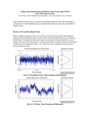
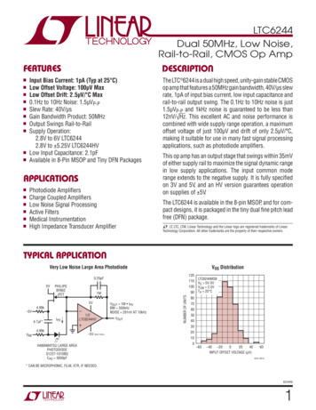
Dual, Low Noise, WidebandVariable Gain AmplifiersAD600/AD602FUNCTIONAL BLOCK DIAGRAMFEATURESAPPLICATIONSUltrasound and sonar time-gain controlsHigh performance audio and RF AGC systemsSignal measurementGENERAL DESCRIPTIONThe AD600/AD6021 dual-channel, low noise, variable gainamplifiers are optimized for use in ultrasound imaging systemsbut are applicable to any application requiring precise gain, lownoise and distortion, and wide bandwidth. Each independentchannel provides a gain of 0 dB to 40 dB in the AD600 and 10 dB to 30 dB in the AD602. The lower gain of the AD602results in an improved signal-to-noise ratio (SNR) at the output.However, both products have the same 1.4 nV/ Hz input noisespectral density. The decibel gain is directly proportional to thecontrol voltage, accurately calibrated, and supply and temperature stable.To achieve the difficult performance objectives, a proprietarycircuit form, the X-AMP , was developed. Each channel of theX-AMP comprises a variable attenuator of 0 dB to 42.14 dBfollowed by a high speed fixed gain amplifier. In this way, theamplifier never has to cope with large inputs and can benefitfrom the use of negative feedback to precisely define the gainand dynamics. The attenuator is realized as a 7-stage R-2Rladder network having an input resistance of 100 Ω, lasertrimmed to 2%. The attenuation between tap points is 6.02 dB;the gain-control circuit provides continuous interpolation betweenthese taps. The resulting control function is linear in dB.1GAT1SCALINGREFERENCEPRECISION PASSIVEINPUT ATTENUATORGATINGINTERFACEC1HIVGA1OPC1LOA1CMGAIN �R-2R LADDER NETWORK62.5ΩRF22.24kΩ (AD600)694Ω (AD602)RF120ΩFIXED-GAINAMPLIFIER41.07dB (AD600)31.07dB (AD602)Figure 1. Functional Block Diagram of a Single Channel of the AD600/AD602The gain-control interfaces are fully differential, providing aninput resistance of 15 MΩ and a scale factor of 32 dB/V (thatis, 31.25 mV/dB) defined by an internal voltage reference. Theresponse time of this interface is less than 1 μs. Each channelalso has an independent gating facility that optionally blockssignal transmission and sets the dc output level to within a fewmillivolts of the output ground. The gating control input isTTL- and CMOS-compatible.The maximum gain of the AD600 is 41.07 dB, and the maximumgain of the AD602 is 31.07 dB; the 3 dB bandwidth of bothmodels is nominally 35 MHz, essentially independent of thegain. The SNR for a 1 V rms output and a 1 MHz noisebandwidth is typically 76 dB for the AD600 and 86 dB for theAD602. The amplitude response is flat within 0.5 dB from100 kHz to 10 MHz; over this frequency range, the group delayvaries by less than 2 ns at all gain settings.Each amplifier channel can drive 100 Ω load impedances withlow distortion. For example, the peak specified output is 2.5 Vminimum into a 500 Ω load or 1 V into a 100 Ω load. For a200 Ω load in shunt with 5 pF, the total harmonic distortion fora 1 V sinusoidal output at 10 MHz is typically 60 dBc.The AD600J/AD602J are specified for operation from 0 C to 70 Cand are available in 16-lead PDIP (N) and 16-lead SOIC packages.The AD600A/AD602A are specified for operation from 40 C to 85 C and are available in 16-lead CERDIP (Q) and 16-lead SOICpackages. The AD600S/AD602S are specified for operation from 55 C to 125 C, are available in a 16-lead CERDIP (Q) package,and are MIL-STD-883-compliant. The AD600S/AD602S are alsoavailable under DESC SMD 5962-94572.Patented.Rev. FInformation furnished by Analog Devices is believed to be accurate and reliable. However, noresponsibility is assumed by Analog Devices for its use, nor for any infringements of patents or otherrights of third parties that may result from its use. Specifications subject to change without notice. Nolicense is granted by implication or otherwise under any patent or patent rights of Analog Devices.Trademarks and registered trademarks are the property of their respective owners.One Technology Way, P.O. Box 9106, Norwood, MA 02062-9106, U.S.A.Tel: 781.329.4700www.analog.comFax: 781.461.3113 2008 Analog Devices, Inc. All rights reserved.00538-0012 channels with independent gain controlLinear in dB gain response2 gain rangesAD600: 0 dB to 40 dBAD602: –10 dB to 30 dBAccurate absolute gain: 0.3 dBLow input noise: 1.4 nV/ HzLow distortion: 60 dBc THD at 1 V outputHigh bandwidth: dc to 35 MHz ( 3 dB)Stable group delay: 2 nsLow power: 125 mW (maximum) per amplifierSignal gating function for each amplifierDrive high speed ADCsMIL-STD-883-compliant and DESC versions available
AD600/AD602TABLE OF CONTENTSFeatures . 1Applications Information . 15Applications . 1General Description . 1Time-Gain Control (TGC) and Time-VariableGain (TVG) . 15Functional Block Diagram . 1Increasing Output Drive. 15Revision History . 2Driving Capacitive Loads . 15Specifications. 3Realizing Other Gain Ranges . 16Absolute Maximum Ratings. 5Ultralow Noise VCA . 16ESD Caution . 5Low Noise, 6 dB Preamplifier . 16Pin Configuration and Function Descriptions . 6Low Noise AGC Amplifier with 80 dB Gain Range . 17Typical Performance Characteristics . 7Wide Range, RMS-Linear dB Measurement System(2 MHz AGC Amplifier with RMS Detector) . 19Theory of Operation . 10Noise Performance . 10Gain-Control Interface . 11Signal-Gating Inputs . 11Common-Mode Rejection . 11100 dB to 120 dB RMS Responding Constant BandwidthAGC Systems with High Accuracy Decibel Outputs . 21100 dB RMS/AGC System with Minimal Gain Error(Parallel Gain with Offset) . 22Achieving 80 dB Gain Range . 11120 dB RMS/AGC System with Optimal SNR(Sequential Gain) . 23Sequential Mode (Maximum SNR) . 12Outline Dimensions . 27Parallel Mode (Simplest Gain-Control Interface) . 13Ordering Guide . 29Low Ripple Mode (Minimum Gain Error) . 13REVISION HISTORY10/08—Rev. E to Rev. FChanges to Power Supply Parameter, Table 1 . 3Changes to Figure 41 . 20Changes to Figure 45 . 21Changes to Figure 47 . 22Changes to Figure 51 . 24Updated Outline Dimensions . 27Changes to Ordering Guide . 295/02—Rev. B to Rev. CChanges to Specifications .2Renumber Tables and TPCs . Global8/01—Rev. A to Rev. BChanges to Accuracy Section of AD600A/AD602A column .21/06—Rev. D to Rev. EUpdated Format . UniversalChanges to Table 2 . 5Changes to The Gain-Control Interface Section . 11Updated Outline Dimensions . 27Changes to Ordering Guide . 283/04—Rev. C to Rev. DChanges to Specifications . 2Changes to Ordering Guide . 3Changes to Figure 3 . 8Changes to Figure 29 . 18Updated Outline Dimensions . 20Rev. F Page 2 of 32
AD600/AD602SPECIFICATIONSEach amplifier section at TA 25 C, VS 5 V, 625 mV VG 625 mV, RL 500 Ω, and CL 5 pF, unless otherwise noted.Specifications for the AD600/AD602 are identical, unless otherwise noted.Table 1.ParameterINPUT CHARACTERISTICSInput ResistanceInput CapacitanceInput Noise Spectral Density 2Noise FigureCommon-Mode Rejection RatioOUTPUT CHARACTERISTICS 3 dB BandwidthSlew RatePeak Output 3Output ImpedanceOutput Short-Circuit CurrentGroup Delay Change vs. GainGroup Delay Change vs. FrequencyTotal Harmonic DistortionACCURACYAD600Gain ErrorMaximum Output Offset Voltage 4Output Offset VariationAD602Gain ErrorMaximum Output Offset Voltage4Output Offset VariationGAIN CONTROL INTERFACEGain Scaling FactorCommon-Mode RangeInput Bias CurrentInput Offset CurrentDifferential Input ResistanceResponse RateConditionsAD600J/AD602J 1MinTyp MaxPin 2 to Pin 3; Pin 6 to Pin 798RS 50 Ω, maximum gainRS 200 Ω, maximum gainf 100 kHzVOUT 100 mV rmsRL 500 Ωf 10 MHz 2.5f 3 MHz; full gain rangeVG 0 V, f 1 MHz to 10 MHzRL 200 Ω, VOUT 1 V peak, RPD 1 kΩ10021.45.323010235275 3250 2 2 60AD600A/AD602A1MinTyp Max95 2.510021.45.323010535275 3250 2 2 60UnitΩpFnV/ HzdBdBdBMHzV/μsVΩmAnsnsdBc0 dB to 3 dB gain3 dB to 37 dB gain37 dB to 40 dB gainVG –625 mV to 625 mVVG –625 mV to 625 mV0 0.5 1 0.5 0.2 0.51010 1 0.505050 0.5 1.0 1.5 0.5 0.2 0.51010 1.5 1.0 0.56565dBdBdBmVmV–10 dB to –7 dB gain–7 dB to 27 dB gain27 dB to 30 dB gainVG 625 mV to 625 mVVG 625 mV to 625 mV0 0.5 1 0.5 0.2 0.555 1 0.503030–0.5 1.0 1.5 0.5 0.2 0.51010 1.5 1.0 0.54545dBdBdBmVmV 3 dB to 37 dB (AD600); 7 dB to 27 dB (AD602)31.73232.330.53233.5dB/V 2.5150 0.75 2.5150VμAnAMΩdB/μs 0.75Pin 1 to Pin 16; Pin 8 to Pin 9Full 40 dB gain changeRev. F Page 3 of 320.351015400.35101540
AD600/AD602ParameterSIGNAL GATING INTERFACELogic Input Low (Output On)Logic Input High (Output Off )Response TimeInput ResistanceOutput Gated OffOutput Offset VoltageOutput Noise Spectral DensitySignal Feedthrough @ 1 MHzAD600AD602POWER SUPPLYSpecified Operating RangeQuiescent CurrentAD600J/AD602J 1MinTyp MaxConditionsAD600A/AD602A1MinTyp Max0.82.4On to off, off to onPin 4 to Pin 3; Pin 5 to Pin 6 1065 4.75111VVμskΩ 400mVnV/ Hz0.330 1065 100 80 70Each channel0.82.40.330 80 70 5.2512.5 4.7511UnitdBdB 5.2514VmASpecifications shown in boldface are tested on all production units at final electrical test. Results from those tests are used to calculate outgoing quality levels. Allminimum and maximum specifications are guaranteed, although only those shown in boldface are tested on all production units.2Typical open- or short-circuited input; noise is lower when the system is set to maximum gain and the input is short-circuited. This figure includes the effects of bothvoltage and current noise sources.3With an additional 1 kΩ pull-down resistor, if RL 500 Ω.4The dc gain of the main amplifier in the AD600 is 113; therefore, an input offset of only 100 μV becomes an 11.3 mV output offset. In the AD602, the amplifier gain is 35.7; therefore, an input offset of 100 μV becomes a 3.57 mV output offset.Rev. F Page 4 of 32
AD600/AD602ABSOLUTE MAXIMUM RATINGSTable 2.ParameterSupply Voltage VSInput VoltagesPin 1, Pin 8, Pin 9, Pin 16Pin 2, Pin 3, Pin 6, Pin 7Pin 4, Pin 5Internal Power DissipationOperating Temperature RangeJ GradeA GradeS GradeStorage Temperature RangeLead Temperature (Soldering, 60 sec)θJA16-Lead PDIP16-Lead SOIC16-Lead CERDIPRating 7.5 V VS 2 V continuous VS for 10 ms VS600 mWStresses above those listed under Absolute Maximum Ratingsmay cause permanent damage to the device. This is a stressrating only; functional operation of the device at these or anyother conditions above those indicated in the operationalsection of this specification is not implied. Exposure to absolutemaximum rating conditions for extended periods may affectdevice reliability.ESD CAUTION0 C to 70 C 40 C to 85 C 55 C to 125 C 65 C to 150 C300 C85 C/W100 C/W120 C/WRev. F Page 5 of 32
AD600/AD602PIN CONFIGURATION AND FUNCTION DESCRIPTIONSC1LO1A1HI2A1LO3GAT1416 C1HI 15 A1CMA114 A1OP–13 VPOSREFGAT25A2LO612 VNEG–11 A2OPA27C2LO810 A2CM AD600 /AD6029C2HI00538-002A2HIFigure 2. Pin ConfigurationTable 3. Pin Function DescriptionsPin scriptionCH1 Gain-Control Input Low. Positive voltage reduces CH1 gain.CH1 Signal Input High. Positive voltage increases CH1 output.CH1 Signal Input Low. Usually connected to CH1 input ground.CH1 Gating Input. A logic high shuts off the CH1 signal path.CH2 Gating Input. A logic high shuts off the CH2 signal path.CH2 Signal Input Low. Usually connected to CH2 input ground.CH2 Signal Input High. Positive voltage increases CH2 output.CH2 Gain-Control Input Low. Positive voltage reduces CH2 gain.CH2 Gain-Control Input High. Positive voltage increases CH2 gain.CH2 Common. Usually connected to CH2 output ground.CH2 Output.Negative Supply for Both Amplifiers.Positive Supply for Both Amplifiers.CH1 Output.CH1 Common. Usually connected to CH1 output ground.CH1 Gain-Control Input High. Positive voltage increases CH1 gain.Rev. F Page 6 of 32
AD600/AD602TYPICAL PERFORMANCE CHARACTERISTICS0.4510.00.359.89.6GROUP DELAY 10.3GAIN CONTROL VOLTAGE (V)0.500538-006GAIN ERROR (dB)0.258.28.0–0.70.7Figure 3. Gain Error vs. Gain Control Voltage–0.5–0.3–0.10.10.3GAIN CONTROL VOLTAGE (V)0.50.7Figure 6. AD600 and AD602 Typical Group Delay vs. VCVG 0V10dB/DIVCENTERFREQ 1MHz10kHz/DIV20dB17dB0 –45 100k1M10MFREQUENCY (Hz)00538-00700538-004–90 100MFigure 4. AD600 Frequency and Phase Response vs. GainFigure 7. Third-Order Intermodulation Distortion, VOUT 2 V p-p, RL 500 Ω10dB7dB0 –45 00538-005–90 100k1M10MFREQUENCY .6–2.8–3.0–3.2–3.4100MFigure 5. AD602 Frequency and Phase Response vs. Gain00538-008NEGATIVE OUTPUT VOLTAGE LIMIT (V)–1.00501002005001000LOAD RESISTANCE (Ω)2000Figure 8. Typical Output Voltage vs. Load Resistance(Negative Output Swing Limits First)Rev. F Page 7 of 32
AD600/AD60210210150mVGAIN 40dBOUTPUT10099GAIN 20dB989790GAIN 0dB96100%00538-009949392100k1M10MFREQUENCY (Hz)5V100ns00538-01295INPUTINPUT IMPEDANCE (Ω)100100MFigure 12. Gating Feedthrough to Output, Gating Off to OnFigure 9. Input Impedance vs. �4–0.7–0.5–0.3–0.10.10.3GAIN CONTROL VOLTAGE (V)0.55V1V VOUT100ns0.7Figure 10. Output Offset Voltage vs. Gain Control Voltage(Control Channel Feedthrough)Figure 13. Gating Feedthrough to Output, Gating On to Off1µs1V1001009090OUTPUTOUTPUT1010Figure 11. Gain Control Channel Response Time. Top: Output Voltage, 2 VMaximum, Bottom: Gain Control Voltage VC 625 mVRev. F Page 8 of 320%100mV500nsFigure 14. Transient Response, Medium and High Gain00538-0141V -010OUTPUT OFFSET VOLTAGE (mV)5
AD600/AD60210AD600: G 20dBAD602: G 10dBBOTH: VCM 100mV rmsVS 5VRL 500ΩTA 25 C5010090–5CMRR igure 15. Input Stage Overload Recovery Time100k1MFREQUENCY (Hz)10M100MFigure 18. CMRR vs. Frequency2010010090–20–30AD602AD600: G 40dBAD602: G 30dBBOTH: RL 500ΩVIN 0VRS 50Ω–60200mV500ns–70–80100k1M10MFREQUENCY 0PSRR (dB)OUTPUT1V100MFigure 19. PSRR vs. FrequencyFigure 16. Output Stage Overload Recovery Time10500mV0–10100CROSSTALK 60200538-0201V00538-017INPUTOUTPUT90AD600: CH1 G 40dB, VIN 0CH2 G 20dB, VIN 100mVAD602: CH1 G 30dB, VIN 0CH2 G 0dB, VIN 316mVBOTH: VOUT 1V rms1, RS 50ΩRL 500ΩCH1 VOUTCROSSTALK 20logCH2 V IN–80–90100k1M10MFREQUENCY (Hz)Figure 17. Transient Response Minimum GainFigure 20. Crosstalk Between A1 and A2 vs. FrequencyRev. F Page 9 of 32100M
AD600/AD602THEORY OF OPERATIONThe signal applied at the input of the ladder network isattenuated by 6.02 dB by each section; thus, the attenuation toeach of the taps is progressively 0 dB, 6.02 dB, 12.04 dB, 18.06 dB,24.08 dB, 30.1 dB, 36.12 dB, and 42.14 dB. A unique circuittechnique is employed to interpolate between these tap points,indicated by the slider in Figure 21, providing continuousattenuation from 0 dB to 42.14 dB.The AD600/AD602 have the same general design and features.They comprise two fixed gain amplifiers, each preceded by avoltage-controlled attenuator of 0 dB to 42.14 dB with independentcontrol interfaces, each having a scaling factor of 32 dB per volt.The AD600 amplifiers are laser trimmed to a gain of 41.07 dB( 113), providing a control range of 1.07 dB to 41.07 dB(0 dB to 40 dB with overlap). The AD602 amplifiers have a gainof 31.07 dB ( 35.8) and provide an overall gain of 11.07 dB to 31.07 dB ( 10 dB to 30 dB with overlap).To understand the AD600/AD602, it helps to think in terms ofa mechanical means for moving this slider from left to right; infact, it is voltage controlled. The details of the control interfaceare discussed later. Note that the gain is exactly determined atall times and a linear decibel relationship is guaranteed automatically between the gain and the control parameter thatdetermines the position of the slider. In practice, the gaindeviates from the ideal law by about 0.2 dB peak (see Figure 28).The advantage of this topology is that the amplifier can usenegative feedback to increase the accuracy of its gain. Inaddition, because the amplifier does not have to handle largesignals at its input, the distortion can be very low. Anotherfeature of this approach is that the small-signal gain and phaseresponse, and thus the pulse response, are essentiallyindependent of gain.Note that the signal inputs are not fully differential. A1LO, A1CM(for CH1), A2LO, and A2CM (for CH2) provide separate accessto the input and output grounds. This recognizes that, even whenusing a ground plane, small differences arise in the voltages atthese nodes. It is important that A1LO and A2LO be connecteddirectly to the input ground(s). Significant impedance in theseconnections reduces the gain accuracy. A1CM and A2CMshould be connected to the load ground(s).Figure 21 is a simplified schematic of one channel. The inputattenuator is a 7-stage R-2R ladder network, using untrimmedresistors of nominally R 62.5 Ω, which results in a characteristicresistance of 125 Ω 20%. A shunt resistor is included at theinput and laser trimmed to establish a more exact inputresistance of 100 Ω 2%, which ensures accurate operation(gain and HP corner frequency) when used in conjunction withexternal resistors or capacitors.NOISE PERFORMANCEGAT1SCALINGREFERENCEPRECISION PASSIVEINPUT ATTENUATORGATINGINTERFACEC1HIVGA1OPGAIN 500ΩR-2R LADDER NETWORK62.5ΩRF22.24kΩ (AD600)694Ω (AD602)RF120ΩFIXED-GAINAMPLIFIER41.07dB (AD600)31.07dB (AD602)00538-0210dBFigure 21. Simplified Block Diagram of a Single Channel of the AD600/AD602The nominal maximum signal at input A1HI is 1 V rms ( 1.4 Vpeak) when using the recommended 5 V supplies, althoughoperation to 2 V peak is permissible with some increase in HFdistortion and feedthrough. Each attenuator is provided with aseparate signal LO connection for use in rejecting commonmode, the voltage between input and output grounds. Circuitryis included to provide rejection of up to 100 mV.An important reason for using this approach is the superiornoise performance that can be achieved. The nominal resistanceseen at the inner tap points of the attenuator is 41.7 Ω (one third of125 Ω), which, at 27 C, exhibits a Johnson noise spectral density(NSD) of 0.84 nV/ Hz (that is, 4kTR), a large fraction of thetotal input noise. The first stage of the amplifier contributesanother 1.12 nV/ Hz, for a total input noise of 1.4 nV/ Hz.The noise at the 0 dB tap depends on whether the input isshort-circuited or open-circuited. When shorted, the minimumNSD of 1.12 nV/ Hz is achieved. When open, the resistance of100 Ω at the first tap generates 1.29 nV/ Hz, so the noiseincreases to 1.71 nV/ Hz. This last calculation would be importantif the AD600 were preceded, for example, by a 900 Ω resistor toallow operation from inputs up to 10 V rms. However, in mostcases, the low impedance of the source limits the maximumnoise resistance.Rev. F Page 10 of 32
AD600/AD602It is apparent from the foregoing that it is essential to use a lowresistance in the design of the ladder network to achieve lownoise. In some applications, this can be inconvenient, requiringthe use of an external buffer or preamplifier. However, very fewamplifiers combine the needed low noise with low distortion atmaximum input levels, and the power consumption required toachieve this performance is quite high (due to the need tomaintain very low resistance values while also coping with largeinputs). On the other hand, there is little value in providing abuffer with high input impedance because the usual reason forthis—the minimization of loading of a high resistance source—is not compatible with low noise.Apart from the small variations just mentioned, the SNR at theoutput is essentially independent of the attenuator setting,because the maximum undistorted output is 1 V rms, and theNSD at the output of the AD600 is fixed at 113 114 nV/ Hz,or 158 nV/ Hz. Therefore, in a 1 MHz bandwidth, the outputSNR is 76 dB. The input NSD of the AD600/AD602 is the samebut, because of the 10 dB lower gain in the AD602’s fixedamplifier, its output SNR is 10 dB better, or 86 dB in a 1 MHzbandwidth.GAIN-CONTROL INTERFACEThe attenuation is controlled through a differential, highimpedance (15 MΩ) input, with a scaling factor that is lasertrimmed to 32 dB per volt, that is, 31.25 mV/dB. Each of thetwo amplifiers has its own control interface. An internal bandgap reference ensures stability of the scaling with respect tosupply and temperature variations and is the only circuitrycommon to both channels.When the differential input voltage VG 0 V, the attenuatorslider is centered, providing an attenuation of 21.07 dB,resulting in an overall gain of 20 dB ( –21.07 dB 41.07 dB).When the control input is 625 mV, the gain is lowered by 20 dB ( 0.625 32) to 0 dB; when set to 625 mV, thegain is increased by 20 dB to 40 dB. When this interface isoverdriven in either direction, the gain approaches either 1.07 dB ( 42.14 dB 41.07 dB) or 41.07 dB ( 0 41.07 dB), respectively.The gain of the AD600 can be calculated byGain (dB) 32 VG 20(1)where VG is in volts.For the AD602, the expression isGain (dB) 32 VG 10(2)Operation is specified for VG in the range from 625 mV dc to 625 mV dc. The high impedance gain-control input ensuresminimal loading when driving many amplifiers in multiplechannel applications. The differential input configurationprovides flexibility in choosing the appropriate signal levelsand polarities for various control schemes.For example, the gain-control input can be fed differentially tothe inputs or single-ended by simply grounding the unusedinput. In another example, if the gain is controlled by a DACproviding a positive-only, ground-referenced output, the gaincontrol LO pin (either C1LO or C2LO) should be biased to afixed offset of 625 mV to set the gain to 0 dB when gain controlHI (C1HI or C2HI) is at zero and to set the gain to 40 dB whenat 1.25 V.It is a simple matter to include a voltage divider to achieve otherscaling factors. When using an 8-bit DAC with an FS output of2.55 V (10 mV/bit), a 1.6 divider ratio (generating 6.25 mV/bit)results in a gain setting resolution of 0.2 dB/bit. The process ofcascading the two sections of an AD600 or AD602 when variousoptions exist for gain control is explained in the Achieving 80 DBGain Range section.SIGNAL-GATING INPUTSEach amplifier section of the AD600/AD602 is equipped with asignal-gating function, controlled by a TTL or CMOS logicinput (GAT1 or GAT2). The ground references for these inputsare the signal input grounds A1LO and A2LO, respectively.Operation of the channel is unaffected when this input is LO orleft open-circuited. Signal transmission is blocked when thisinput is HI. The dc output level of the channel is set to within afew millivolts of the output ground (A1CM or A2CM), andsimultaneously the noise level drops significantly. The reductionin noise and spurious signal feedthrough is useful in ultrasoundbeam-forming applications, where many amplifier outputs aresummed.COMMON-MODE REJECTIONA special circuit technique provides rejection of voltagesappearing between input grounds (A1LO and A2LO) andoutput grounds (A1CM and A2CM). This is necessary becauseof the op amp form of the amplifier, as shown in Figure 21.The feedback voltage is developed across the RF1 resistor(which, to achieve low noise, has a value of only 20 Ω). Thevoltage developed across this resistor is referenced to the inputcommon, so the output voltage is also referred to that node.For zero differential signal input between A1HI and A1LO, theoutput A1OP simply follows the voltage at A1CM. Note that therange of voltage differences that can exist between A1LO andA1CM (or A2LO and A2CM) is limited to about 100 mV.Figure 18 shows the typical common-mode rejection ratio vs.frequency.ACHIEVING 80 dB GAIN RANGEThe two amplifier sections of the X-AMP can be connected inseries to achieve higher gain. In this mode, the output of A1(A1OP and A1CM) drives the input of A2 via a high-passnetwork (usually just a capacitor) that rejects the dc offset.The nominal gain range is now –2 dB to 82 dB for the AD600or 22 dB to 62 dB for the AD602.Rev. F Page 11 of 32
AD600/AD60285There are several options in connecting the gain-control inputs.The choice depends on the desired SNR and gain error (outputripple). The following examples feature the AD600; thearguments generally apply to the AD602, with appropriatechanges to the gain values.807570SNR (dB)65SEQUENTIAL MODE (MAXIMUM SNR)In the sequential mode of operation, the SNR is maintained atits highest level for as much of the gain control range aspossible, as shown in Figure 22. Note here that the gain range is0 dB to 80 dB. Figure 23, Figure 24, and Figure 25 show thegeneral connections to accomplish this. Both gain-controlinputs, C1HI and C2HI, are driven in parallel by a positive-only,ground-referenced source with a range of 0 V to 2.5 VGFigure 22. SNR vs. Control Voltage Sequential Control (1 MHz Bandwidth)An auxiliary amplifier that senses the voltage differencebetween input and output commons is provided to reject thiscommon 4dB1.07dBC1LOC2HIVG1VG2VO1 0.592VVC O2 1.908VFigure 23. AD600 Gain Control Input Calculations for Sequential Control Operation 6dBC2HIC1LO41.07dBC2LOVG2VG1VO1 0.592VVO2 1.908VVC 1.25VOUTPUT40dB00538-055INPUT0dB–1.07dBFigure 24. AD600 Gain Control Input Calculations for Sequential Control Operation 2VG1VC 2.5V41.07dBC2LOVO1 0.592VVO2 1.908VFigure 25. AD600 Gain Control Input Calculations for Sequential Control Operation (C)Rev. F Page 12 of 32OUTPUT80dB00538-056INPUT0dB38.93dB
AD600/AD602The gains are offset such that the gain of A2 is increased onlyafter the gain of A1 has reached its maximum value (see Figure 26).Note that, for a differential input of 700 mV or less, the gain ofa single amplifier (A1 or A2) is at its minimum value of 1.07 dB;for a differential input of 700 mV or more, the gain is at itsmaximum value of 41.07 dB. Control inputs beyond theselimits do not affect the gain and can be tolerated without damage orfoldover in the response. See the Specifications section for moredetails on the allowable voltage range. The gain is nowGain (dB) 32 VC(3)where VC is the applied control voltage. 40.56dB* 1.07dB–0.56dBAs shown in Figure 28 and Figure 29, the output ripple isperiodic. By offsetting the gains of A1 and A2 by half theperiod of the ripple, or 3 dB, the residual gain errors of the twoamplifiers can be made to cancel.
The maximum gain of the AD600 is 41.07 dB, and the maximum gain of the AD602 is 31.07 dB; the 3 dB bandwidth of both models is nominally 35 MHz, essentially independent of the gain. The SNR for a 1 V rms output and a 1 MHz noise bandwidth is typically 76 dB for the AD600 and 86 dB for the AD602. The amplitude response is flat within 0.5 dB .