Transcription
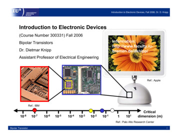
Introduction to Electronic Devices, Fall 2006, Dr. D. KnippIntroduction to Electronic Devices(Course Number 300331) Fall ipp/Bipolar TransistorsDr. Dietmar KnippAssistant Professor of Electrical EngineeringSource: AppleRef.: AppleRef.: ension (m)Ref.: Palo Alto Research CenterBipolar Transistor1
Introduction to Electronic Devices, Fall 2006, Dr. D. KnippIntroduction to Electronic Devices5 Bipolar Transistors5.1 Introduction5.2 Basic transistor operation5.3 Transistor under zero bias5.4 Transistor under bias conditions5.4.1 Shockley Assumptions5.4.2 The ideal transistor equation5.4.3 The transistor equation in its general form5.4.4 Modes of Operation5.8.1 The active mode5.8.2 The Saturation mode5.8.3 The cutoff mode5.8.4 The inversion mode5.5 Transport and gain factors5.5.1 The Emitter efficiency5.5.2 The Transport factor5.5.3 The Common-base current gain5.5.5 The summary of the transport and gain factorsBipolar Transistor2
Introduction to Electronic Devices, Fall 2006, Dr. D. Knipp5.6 Transistor Design5.6.1 The transport factor5.6.2 The Emitter Efficiency5.7 Bipolar Transistors as Amplifiers5.7.1 Common base circuit5.7.2 Common emitter circuit5.7.3 The Early Effect5.8 Transfer characteristic and gain5.9 Device parameters5.10 Equivalent circuit of a bipolar junction transistorReferencesBipolar Transistor3
Introduction to Electronic Devices, Fall 2006, Dr. D. Knipp5.1 IntroductionThe transistor (Germanium point contact transistor) was invited by Barttain,Bardeen and Shockley in 1947. As the name already implies it is a bipolardevice (like a diode), which means that both electrons and holes (minority andmajority carriers) contribute to the overall current flow.The bipolar junction transistor (BJT) is one of the most importantsemiconductor devices. The transistor is used for high speed circuits, analogcircuits and power applications.The underlying electronic transport mechanisms of bipolar junction transistors(BJT) and diodes are similar. Both devices are diffusion controlled devices.Therefore, the influence of the drift current on the total current is negligible.The operating principle of bipolar devices is different from the behavior ofunipolar device like a Field Effect Transistors (FETs), where the current iseither controlled by electrons or holes. Furthermore, a field effect transistor is adrift controlled electronic device.Bipolar Transistor4
Introduction to Electronic Devices, Fall 2006, Dr. D. Knipp5.1 IntroductionA bipolar transistor (like all othertransistors) is a three (four) terminaldevice. The device consists of an inputand an output loop. The device isdesigned in such a ways that small inputchanges of a current or/and a voltageresult in large changes of the outputcurrent or/and voltage.The BJT device structure consists of twopn junctions. The device can beimplemented as an pnp or a npnstructure. Each of the doped regions isconnected with one of the terminals:Base, Emitter or Collector. The threeregions of a BJT are formed by thediffusion of a doping profiles in asubstrate.Schematic cross section of a pnptransistor. The transistor isimplementedinap-typesubstrate. The n-type and the p type regions are formed bydiffusion of dopants in the p-typesubstrate. The electrodes areformed by metal contacts.Ref.: M.S. Sze, Semiconductor DevicesBipolar Transistor5
Introduction to Electronic Devices, Fall 2006, Dr. D. Knipp5.1 IntroductionThe operation principle of a bipolar transistor relies on the fact that the baseregion of the transistor is a very thin region, so that the two diodes affect eachother. The thickness of the base in controlled by the manufacturing (diffusion)process.In terms of applications pure analog integrated circuits are getting less important.Nowadays the technology shifts towards BiCMOS technology. BiCMOS is acombination of bipolar technology and metal oxide semiconductor technology(technology required to manufacture field effect transistors). It allows therealization of analog and digital circuits on a single chip.5.2 Basic transistor operationThe two possible device structures of a bipolar transistor or Pnp- and a npnstructures. Bipolar transistors can operate in four modes of operation,depending on the voltage applied to the base-emitter and the base-collectorjunction. The four modes of operation are: Active mode, inversion mode,cutoff mode, Saturation mode.Bipolar Transistor6
Introduction to Electronic Devices, Fall 2006, Dr. D. Knipp5.2 Basic transistor operationIn order to realize an amplifier the BJTwill be operated in the active mode. Inthe following the basic operating principleof a bipolar transistor in the active modewill be presented.The and – signs indicate the polaritiesof the voltages applied to the terminalsunder normal operating conditions (activemode).pnp-transistorIn the active mode the emitter base diodeis forward biased (VEB 0) and the basecollector diode is reverse biased (VCB 0).npn-transistorRef.: M.S. Sze, Semiconductor DevicesBipolar Transistor7
Introduction to Electronic Devices, Fall 2006, Dr. D. Knipp5.2 Basic transistor operationOn this slide the and – signsindicate the direction of the currentflow.I B I E ICThe npn-structure is complementaryto the pnp structure. As aconsequence the current flow andthe voltage polarities are reversed.In the following we will discuss theelectronic transport of a pnptransistor.pnp-transistornpn-transistorRef.: M.S. Sze, Semiconductor DevicesBipolar Transistor8
Introduction to Electronic Devices, Fall 2006, Dr. D. Knipp5.3 Bipolar Junction Transistors under zero baisAt first the BJT will be studied in thermal equilibrium. All three terminals of thedevice are grounded.Under thermal equilibrium the Fermi level is constant throughout the entire devicestructure. As a consequence the derivative of the Fermi level is zero, so that theoverall current flowing through the device is zero.The following device structure is used for the discussion: The emitter is (much)heavier doped than the base and the base is again heavier doped than thecollector. The base region is much shorter than the emitter and the collectorregion. The base width of the base region is much shorter than the diffusionlength of the minority carriers. Therefore, the two pn-junctions affect each other.If the base-region would be much longer than the diffusion length of the minoritycarriers in the base region of the two pn-junctions would behave like two separatediodes. The operation of the diodes would be independent of each other.The electric field distribution in the BJT can be calculated by solving the Poissonequation. As a consequence of the doping profile in the individual regions of thedevice the maximum electric field and the built-in voltage for the base/emitterjunctions is higher than the maximum electric field and the built-in voltage for thebase/collector junction (under thermal equilibrium).Bipolar Transistor9
Introduction to Electronic Devices, Fall 2006, Dr. D. Knipp5.3 Bipolar Junction Transistorunder zero biasThroughout the following discussion it isassumed that two abrupt junctions areformed. As a consequence the electric fielddistribution outside of the depletion regionsis zero.The formation of the space charge regionfor a BJT is comparable with the formationof the space charge region of a diode.pnp-transistor(a) pnp-transistor under thermal equilibrium(all terminals grounded).(b) Doping profile of an abrupt pnp structure,(c) Electric field profile,(d) Energy band diagramRef.: M.S. Sze, Semiconductor DevicesBipolar Transistor10
Introduction to Electronic Devices, Fall 2006, Dr. D. Knipp5.3 Bipolar Junction Transistor under zero biasThere are technological and a physical reasons for the different doping profilesin the individual regions of the device:Technological:The fabrication of a BJT requires two diffusion steps to form three regions withdifferent doping concentrations. In the first diffusion step the base has to beformed and the already existing dopants in the material (in the substrate) haveto be compensated or over compensated. In the second diffusion step thedoping concentration has to be increased again to compensate theincorporated dopants of the first diffusion step.Physical:The goal of the transistor design is the realization of transistors with highcurrent and/or voltage gain. High current and voltages gains can be achieved ifthe doping concentration in the base is lower than the doping concentration inthe emitter. The underlying physical reasons for this particular behavior will bediscussed in the chapter on transport and gain factors.Bipolar Transistor11
Introduction to Electronic Devices, Fall 2006, Dr. D. Knipp5.4 Transistor under bias conditionsBefore deriving the ideal bipolar junction transistor equations the basicoperating principle of BJT under biasing conditions will be described. Here wewill concentrate on a common base bipolar transistor in active mode as this isthe most important mode of operation. In this case the base/emitter junction isin forward bias and the base/collector junction operates under reverse biasconditions. The input and the output loop share the base terminal. Therefore,the circuit is called a common base circuit.As a consequence of the applied bias voltages the width of the depletionregions is changed. Since the base emitter junctions is under forward biasholes are injected via the emitter and electrons are injected via the base. At thesame time the base collector junction is reverse biased and the current flowshould be small. However, as the width of the base region is very short theholes injected in the emitter diffuse through the base so that they reach thebase collector depletion region, where the holes „float up“ into the collectorregion. Therefore, the collector collects the holes „floating up“. The emitter iscalled emitter because holes are emitted, which are collected by the collector(BJT in the active mode). Most of the emitted holes reach the collector region.Bipolar Transistor12
Introduction to Electronic Devices, Fall 2006, Dr. D. Knipp5.4 Transistor under bias conditionsDue to the forward bias applied to thebase/emitter junction the external electric fieldlowers the electric field caused by the built-involtage. The width of the space charge regionand the electric field is reduced.The opposite behavior is observed for thereverse biased diode. Here the externalelectric field enhances the internal electricfield, so that the width of the space chargeregion is extended.(a) pnp-transistor under biasconditions. The transistor operatesin the active mode.(b) Doping profile of an abrupt pnpstructure,(c) Electric field profile,(d) Energy band diagramBipolar TransistorRef.: M.S. Sze, Semiconductor Devices13
Introduction to Electronic Devices, Fall 2006, Dr. D. Knipp5.4 Transistor under bias conditionsDue to the applied bias voltages the Fermi level split up into quasi Fermi levels.For the pn junction under forward bias the quasi Fermi levels shift closer to thecorresponding bands. This means that the quasi Fermi level for the electronsshift closer to the conduction band, whereas the quasi Fermi level for the holesshifts closer to the valence band. For the reverse bias diode the oppositebehavior is observed. The Quasi Fermi levels shift away from thecorresponding bands, because the product of the carrier concentration is belowthe square of the intrinsic carrier concentration.Bipolar Transistor14
Introduction to Electronic Devices, Fall 2006, Dr. D. Knipp5.4.1 Shockley AssumptionsIn order to derive the ideal transistor equation the Shockley assumptions have tobe fulfilled. The assumptions for deriving the ideal transistor equations arecomparable with the assumptions used for deriving the ideal diode equation. Uniform doping throughout the individual regions of the device, so that abruptjunctions are formed at the emitter/base and the collector/base interface. The hole drift current in the base region and the collector saturation current arenegligible. Low-level injection for the forward biased diodes Non losses due to generation and recombination in the depletion regions of thebase/emitter junction and the base/collector junction No series resistance in the device (No voltage drop across the neutral regions.)Bipolar Transistor15
Introduction to Electronic Devices, Fall 2006, Dr. D. Knipp5.4.2 The ideal transistor equationIn the active mode the base/emitter junction is forward biased and thebase/collector junction is reverse biased.Under forward bias conditions of the base emitter diode holes are injectedfrom the emitter region into the base region. Subsequently the holes diffuseacross the base region and reach the collector junction.In order to determine the ideal transistor equation the Diffusion equation hasto be solved. It can be assumed that the current flow in the base isdetermined by the diffusion rather than the drift of carriers. As a consequencethe electric field in the base can be ignored.The Diffusion equation has to be solved for the forward biased base/emitterjunction which can be described by an asymmetric pn-junction. 2 pn p n p n 0Dp 02τ pl xBipolar TransistorDiffusion equation for holes16
Introduction to Electronic Devices, Fall 2006, Dr. D. Knipp5.4.2 The ideal transistor equationFirstly we determine the minority carrier distribution (i.e. hole concentration inthe n-type base region). In a second step the current flow can be obtainedfrom the minority-carrier gradient.The general solution of the Diffusion equation is given by x x pn ( x ) pn 0 C1 exp B C2 exp B L L pp where Lp and Ln are the hole and the electron diffusion length of the minoritycarriers.L p D pτ plHole diffusion lengthLn Dnτ nlElectron diffusion lengthBipolar Transistor17
Introduction to Electronic Devices, Fall 2006,
The bipolar junction transistor (BJT) is one of the most important semiconductor devices. The transistor is used for high speed circuits, analog circuits and power applications. The underlying electronic transport mechanisms of bipolar junction transistors (BJT) and diodes are similar. Both devices are diffusion controlled devices.


