Transcription
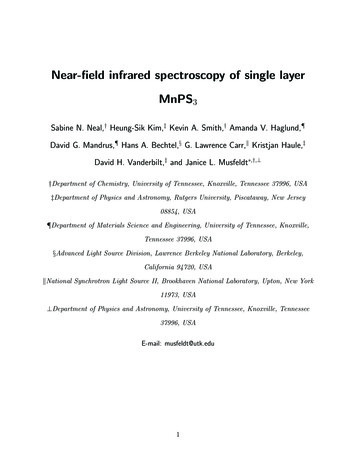
Near-field infrared spectroscopy of single layerMnPS3Sabine N. Neal,† Heung-Sik Kim,‡ Kevin A. Smith,† Amanda V. Haglund,¶David G. Mandrus,¶ Hans A. Bechtel,§ G. Lawrence Carr,k Kristjan Haule,‡David H. Vanderbilt,‡ and Janice L. Musfeldt ,†, †Department of Chemistry, University of Tennessee, Knoxville, Tennessee 37996, USA‡Department of Physics and Astronomy, Rutgers University, Piscataway, New Jersey08854, USA¶Department of Materials Science and Engineering, University of Tennessee, Knoxville,Tennessee 37996, USA§Advanced Light Source Division, Lawrence Berkeley National Laboratory, Berkeley,California 94720, USAkNational Synchrotron Light Source II, Brookhaven National Laboratory, Upton, New York11973, USA Department of Physics and Astronomy, University of Tennessee, Knoxville, Tennessee37996, USAE-mail: musfeldt@utk.edu1
AbstractIn order to explore the properties of a complex van der Waals material underconfinement, we measured the near-field infrared response of the magnetic chalcogenideMnPS3 in bulk, few-, and single-layer form and compared the results with traditionalfar field vibrational spectroscopy and complementary lattice dynamics calculations.Trends in the activated Bu mode near 450 cm 1 are particularly striking, with thedisappearance of this structure in the thinnest sheets. Combined with the amplifiedresponse of the Ag mode and analysis of the Au Bu features, we find that symmetryis unexpectedly increased in single-sheet MnPS3 . The monoclinicity of this system istherefore a consequence of the long-range stacking pattern rather than local structure.C2/m540(nm)4002001 µm0Near-field Amplitude A(ω)Table of contents entry:P31mbulkmonolayer400500600-1Frequency (cm )Keywords: near-field infrared spectroscopy, magnetic chalcogenide, MnPS3 , atomicallythin layer, symmetry analysis2
IntroductionThe layered structures of many chalcogenides allow for exfoliation, providing a unique platform for combining the complexity of bulk materials with the tunability of few- and singlelayer systems. 1 One of the most widely investigated van der Waals materials is MoS2 . 2–5Major findings include the indirect direct gap crossover at the single layer level, 3,4 valleysplitting effects driven by spin-orbit coupling, 6,7 and the confinement and symmetry-breakingeffects that lead to unique chemical, electronic, optical, and thermal properties. 8–11 Complex chalcogenides are also attracting attention. 8,12 One of the most interesting initiativesinvolves the creation of robust, single-layer magnetic semiconductors like CrI3 , CrSiTe3 , andMnPS3 . 13–16 One commonality between all of these systems - from MoS2 to MnPS3 - isthe role of Raman scattering to assure sample quality, probe even-symmetry vibrationalmodes, and explore confinement effects in the single layer. 5,17,18 The ungerade modes are,however, completely unexplored in few layer systems. Infrared spectroscopy is well suitedfor examining the fundamental excitations of the lattice, and because the technique probesodd-symmetry vibrations, it is useful for uncovering ferroelectric, vibronic, and spin-latticecoupling mechanisms. 19–22 Although it is highly desirable to extend toward few- and singlelayer systems, traditional infrared spectroscopy cannot beat the diffraction limit for smallsized (exfoliated) samples. 23Synchrotron-based infrared nanospectroscopy offers a path forward. The technique combines a high brightness, broadband synchrotron light source 24 with Fourier transform techniques and a tip-enhanced approach to enable spectroscopic work on small-sized samplesand materials with micro- and nano-scale texture. 23,25–27 The spatial resolution, achieved byfocusing infrared light onto an atomic force microscope (AFM) tip [Fig. 1(c)], is on the orderof 20 20 nm2 . Initially, this technique was confined to the middle infrared 23 and provedpowerful for exploring polaritons in graphene, unveiling the inhomogeneous character of thephase transition in VO2 , and studying heterogeneity in Bi2 Se3 and Sb2 Se3 nanocrystals. 28–31Recently, the operational window has been expanded into the far infrared - down to 3303
cm 1 . 25 Near-field infrared spectroscopy is therefore inviting new approaches to studyingchalcogenides. This is because many (but not all) of the characteristic vibrational modes ofthese materials resonate in this frequency window. What distinguishes synchrotron-basednear-field spectroscopy from tip-enhanced Raman scattering is the ability to explore odd(rather than even-) symmetry vibration modes. 328 9 8:9inf8#93455 7n !"#n !"n !""n !!"n !",,-()%* .,,-n !"! µ"-ra redlig# %&'()*) ht1 02(),-(./ 0' - )' 150Height (nm)Figure 1: (a) Crystal structureof monoclinic MnPS3 showing theslab thickness and inter-layer distance.(b) Local structure formonolayer MnPS3 emphasizing thebonding around the Mn center and 3456/ 7the P-P dimer. 33 (c) Close-upschematic of the near-field setupshowing the cantilever tip directing light to focus on a small areaof the sample. Spatial resolution is 8.9on the order of 20 20 nm2 . (d)High resolution AFM image alongwith the corresponding layer number, extracted from (e) the heightprofile analysis along the red linein (d).10050020004000!"# %&'( )%* We selected MnPS3 as a platform with which to examine these ideas. This compound belongs to a large family of metal phosphorus trichalcogenides with the formula M PX3 whereM metal ion, in this case high spin Mn2 (S 52 ), and X chalcogenide. This system is anon-collinear antiferromagnet below TN 78 K. It is also ferrotoroidic. 34 M PX3 compoundscan be viewed as salts of the phosphate anion, with Mn2 cations and (P2 S6 )4 anions. Thesecations are linked together by Mn-X bonds, which are weaker than the bonds in the anionunit. This allows for a conceptual division of vibrational features into internal modes ofthe anion unit and external modes from the interactions between cation and anion. 35 Figure1(a) shows the stacking of MnPS3 into a monoclinic van der Waals solid. 33 The individuallayer thickness is 3.22 Å, with each layer separated by a van der Waals gap of 3.27Å. The local structure [Fig. 1(b)] is especially sensitive to symmetry. Rather than C2/m4
like the bulk, the monolayer is proposed to be P3̄1m - assuming that the internal structureremains intact. 36 At this time, the possibility is untested. While extensive investigationof Raman scattering and light emission reveals strong electron-phonon coupling, 5,37 the infrared response of this system in few layer form is wholly unexplored. Because the behaviorof ungerade vibrational modes is crucial for uncovering local structure modifications, testingvarious subgroup candidates, and developing higher-level functionalities like ferroelectricity, 19,38–40 bringing infrared spectroscopy to the field of few- and single-layer chalcogenidesis an important step forward.In order to explore odd-symmetry vibrational modes in few- and single-layer complexchalcogenides, we measured the near-field infrared response of MnPS3 and compared ourfindings to first principles calculations. We find that features in the near-field spectrum ofthe single crystal are a combination of both infrared- and Raman-active modes. This mixedactivation is a consequence of the tip-based nature of the technique. Detailed analysis ofthe near-field spectra supports a sized-induced symmetry crossover. The behavior of the Bumode is most revealing. It is amplified in the n 142 - 48 range but disappears below n 11, indicative of a symmetry increase in few-sheet samples. Here, n is the layer number.Thus, single layer MnPS3 is actually higher symmetry than previously supposed. This isinteresting because local and long-range symmetry determine functionality in a variety ofmaterials.Results and discussionFigure 2 summarizes the vibrational properties of single crystalline MnPS3 . In addition tothe traditional infrared absorption, Raman scattering, and the theoretically-predicted modepositions, it also displays our near-field results. Combined with prior literature 41 and latticedynamics calculations, we can assign all of the peaks in these spectra. Focusing first onthe conventional infrared and Raman response, we assign the strong infrared band at 5735
-1Absorption (cm )(a)Raman Intensity(Arb. de A(ω)Bu(c)350Near-fieldPhase ϕ(ω) (deg.)Figure 2: (a) Traditional infrared absorption (green) and Raman scattering (red) spectra at 300K. (b) Lattice dynamics calculations of MnPS3 projected according to mode symmetry. Recall thatthe ungerade modes are infraredactive, and the gerade symmetrymodes are Raman-active. The calculated frequencies are within 3%of the experimental peak positions.The calculated modes are shownwith a Gaussian line shape and 2cm 1 broadening. The higher peakintensity indicates near degeneracy. (c) Room temperature nearfield amplitude (blue) and phase(orange) spectra for single crystalline MnPS3 . We set the overall frequency scale to focus on theavailable near-field energy window.400450500550600650-1Frequency (cm )cm 1 to the nearly degenerate PS3 stretching mode. The presence of two weak Ramanbands at 569 and 581 cm 1 shows that coupling between two PS3 units is weak. The smallinfrared-active Bu mode at 452 cm 1 is a combination of a P-P stretch out-of-plane PS3translation. The strongest Raman band near 385 cm 1 is due to a symmetric stretch of PS3 ,largely ascribed to the motion of chalcogen atoms with a weak contribution from vibrationalcoupling between the phosporus and sulfur units. 41 As expected, the Mn-containing modesappear at lower frequencies. They are not included here in order to focus on the currentlyavailable frequency window. 25 Our assignments are summarized in Table 1.Figure 2(c) displays the near-field spectrum of single crystalline MnPS3 - both amplitudeand phase - prior to exfoliation. Assignments are made by comparison with the aforementioned infrared and Raman spectroscopies as well as our calculated mode frequencies anddisplacement patterns. Clearly, the infrared-active modes are well represented in terms ofposition, shape, and amplitude confirming the effectiveness of the near-field technique. For6
instance, the Au Bu modes centered near 573 cm 1 are present in both sets of spectra, withthe much smaller Bu mode increasing in intensity in the near-field response. At the sametime, there are additional features that are not anticipated according to traditional selectionrules. For instance, there is a subtle hint of the 360 cm 1 mode in the near-field spectrumthat is likely an activated Ag mode - normally present in the Raman response. We thereforesee that tip-enhanced infrared spectroscopy does not fully conform to traditional selectionrules. This is because of tip curvature, the shape of the electric field lines, and penetrationdepth differences of the tip-enhanced technique. 42 Taken together, these assignments placenear-field infrared spectroscopy of MnPS3 on a firm foundation from which we can extendtoward few- and single-layer systems.Table 1: Vibrational mode assignments of single crystalline MnPS3 . All values are in cm 1ω (infrared)–452ω (Raman)385–573––569, 581ω (near-field)* assignment355ν(PS3 )450T 0 z (PS3 ) ν(P-P)567ν(PS3 )–ν(PS3 )ν symmetric stretch, T 0 translational motion, * Corresponds to maxima in the phase spectra.As part of this work to measure few- and single-layer MnPS3 , we tested a variety ofsubstrates for suitability with our target material. These included gold, aluminum, glass,sapphire, and silicon. The choice turns out to be crucial. 43 Our work with uncoated goldmirrors revealed excellent adhesion of few- and single-sheet MnPS3 via gold· · · surfur interactions. This not only eliminates the need for glue but also the interference of substratephonons. The use of bare gold mirrors to support exfoliated chalcogenides does, however,have the disadvantage of introducing a small charge transfer band between the sulfur andthe gold centered at 550 cm 1 . 44 This charge transfer excitation is somewhat problematicfor MnPS3 because it partially obscures some of the sulfur-related stretching modes between550 and 600 cm 1 . We anticipate that uncoated gold will, however, work well for some ofthe heavier chalcogenides like MoTe2 where the frequencies are shifted downward due to7
heavier masses. 45 In any case, the charge transfer band is apparent only in the single-layerresponse for MnPS3 . We attempted to uncover the hidden Au Bu phonon by modelingthis Au· · · S charge transfer with a series of Voigt oscillators and subtracting the result fromthe near-field spectrum. This procedure did not, unfortunately, reveal the superimposedphonons - probably due to their small oscillator strength. This limits the frequency windowfor single-layer MnPS3 - although bilayer and above is relatively unaffected.Turning our attention back to the magnetic chalcogenide, Fig. 3 summarizes the nearfield infrared response of MnPS3 at various layer thicknesses. The spectra and theoreticallypredicted phonon pattern of the bulk crystal and monolayer in Fig. 3(a) reveal a stunningdissimilarity. Figure 3(b, c) shows a more systematic view of the near-field infrared responseof MnPS3 as a function of layer number (n). The gold· · · sulfur interaction is particularlyapparent in the single layer (n 1) spectrum as evidenced by the charge transfer band above550 cm 1 . 44 The symmetry relationship between C2/m and P3̄1m is summarized in Fig3(d). Remarkably, the vibrational response demonstrates that MnPS3 single crystal haslower symmetry than few- and single-sheet analogs.Detailed analysis of the near-field spectra [Fig. 3(b,c)] supports a size-induced symmetrycrossover. The behavior of the Bu feature at 450 cm 1 is most revealing. This structure isrelatively modest in the bulk (n ), increases slightly in intensity and blueshifts at intermediate sheet thicknesses, diminishes again, and disappears entirely below n 11. It neverreappears - even at the monolayer - indicating that the symmetry for n 11 is no longerC2/m. Further, the symmetry must be higher, not lower, for this feature to disappear.To clarify the nature of the disappearance of the 450 cm 1 peak, calculated phonon frequencies from two separate single-layer structures with monoclinic and hexagonal symmetryconstraints are shown in Fig 3(d). Note that the modes around 450 cm 1 , which exist inthe monoclinic symmetry, are absent in the hexagonal case, indicating this feature is indeedlinked to the restoration of three-fold symmetry in the single-layer limit.The Ag mode near 376 cm 1 provides additional evidence for a change in symmetry. This8
(b)ExperimentalAgBuAu Bun monolayern n 11n 142n 6n 63n 61n 48n 44n 30n 22TheoryP 31m400500-1600n 16400Frequency (cm )500-1Near-field Amplitude A(ω)TheoryC2/mNear-field Amplitude A(ω)I (a.u.) Near-field Amplitude A(ω) I (a.u.)(a)(c)n 5n 4n 3n 2monolayer600400500600-1Frequency (cm )Frequency (cm )(d)C2/mP 31m100200300400-1500600Frequency (cm )Figure 3: (a) Near-field infrared response of MnPS3 single crystal compared with that of themonolayer. Corresponding lattice dynamics calculations highlight the symmetry modifications. We show both the infrared- and Raman-active modes. (b,c) Evolution of the near-fieldinfrared spectra from MnPS3 single crystals (n ) to the monolayer. The exfoliated sheetsare on a gold substrate. In (b) and (c), the spectra are shifted (by a constant amount) forclarity. (d) Direct comparison of the predicted vibrational modes over the entire frequencyrange for a single sheet of MnPS3 - depending on the symmetry that was imposed during thecalculation (C2/m vs.P3̄1m).feature is at the limit of our sensitivity in the bulk, becomes somewhat more apparent inthe intermediate thickness range, and is fairly clear in the n 11 spectrum. The trends areless obvious in few layer systems except the Ag mode (now actually A1g 46 ) which appearsclearly and is even amplified in the monolayer spectrum. The Au Bu sulfur-phosphorousstretching modes near 556 cm 1 also display signatures of a thickness-dependent symmetrytransition. This feature is strong and fairly wide in the bulk - as expected when a numberof closely-related modes overlap. The structure evolves with decreasing thickness sportinga clear doublet between n 142 and 48. The low frequency branch of the doublet redshifts9
with decreasing thickness whereas the high frequency branch blueshifts slightly. The doubletbroadens significantly between n 44 and 22. Between n 16 and 11, the two branches cometogether somewhat and begin to diminish. Below n 11, the features are much more diffuseand eventually (n 1) overcome by the gold· · · sulfur charge transfer band above 550 cm 1 . 44A combined analysis of the near-field spectra and lattice dynamics calculations substantiatethe connection between decreasing layer number and a crossover to higher symmetry.It is curious that three-fold symmetry is restored below n 11 rather than at n 1 wherethe stacking becomes irrelevant. We speculate that, since interactions between adjacent layers in this wide-gap ( 2.65 eV) semiconductor are weak, 47 thermal excitations may restorethe higher symmetry below a critical thickness - especially at room temperature. Additionalquestions relate to stabilizing crystal structures with different stacking symmetries for distinct physical properties in these layered systems as a function of layer thickness or alternategrowth conditions. This is important because certain stacking patterns may give rise todistinct magnetic order or even complex order parameters such as ferrotoroidicity. 34 In thisregard, synchrotron-based near-field spectroscopy will become a crucial tool for exploringfew-layer van der Waals compounds and ultrathin oxide heterostructures.ConclusionSynchrotron-based near-field infrared spectroscopy provides a unique platform for evaluatingcomplex chalcogenides like MnPS3 . As discussed in detail throughout the text, this techniqueis a fusion of a high brightness source, Fourier transform techniques, and a tip to localizethe radiation. To complement this revolutionary spectroscopic approach, we also developeda general method for stabilizing complex chalcogenides in few- and single-sheet form onto abare gold substrate. That method is outlined here and then utilized to reveal the dynamicsof our target material MnPS3 in few- and single layer form. Traditional infrared absorptionand Raman scattering as well as complementary first principles lattice dynamics calcula-10
tions supported this effort. Near-field measurements reveal a dramatic change in spectralcharacteristics under confinement. Perhaps the most striking trend involves the Bu modenear 450 cm 1 which disappears almost completely in the thinnest sheets. Combined withthe amplified response of the Ag mode and analysis of the Au Bu features, we find thatsymmetry is unexpectedly increased, rather than decreased, in monolayer MnPS3 . The monoclinicity of this system is thus a consequence of long-range stacking patterns rather than thelocal structure. One test of this supposition is how the symmetry crossover changes in theMnPS3 , NiPS3 , and FePS3 series - a subject of future work. Near-field infrared spectroscopytherefore has the potential to unlock a much wider field of investigation into the propertiesof atomically-thin materials.MethodsSingle crystals of MnPS3 were prepared via chemical vapor transport as described previously. 48 Surface-exfoliated crystals were mounted on pin-hole apertures for both infraredand Raman measurements. Traditional far-field infrared studies were performed on a BrukerIFS 113v Fourier-infrared spectrometer equipped with a bolometer detector over the 20-700cm 1 frequency range with resolution of 2 cm 1 . The measured transmittance was convertedto absorption as α(ω) - d1 ln(T (ω)), where T (ω) is measured transmittance and d is thickness. No attempt was made to do a reflectance correction to the transmittance. Ramanscattering was performed on a LabRAM HR Evolution Raman spectrometer (50-700 cm 1 )using an excitation wavelength of 532 nm at a power of 0.5 mW with an 1800 line/mmgrating.Synchrotron-based near-field infrared spectroscopy was performed using a commercialnanoscope (neaSNOM, Neaspec GmbH) using the setup at beamline 2.4 at the AdvancedLight Source at Lawrence Berkeley National Laboratory. 23 Both amplitude and phase datawere collected over the 330-700 cm 1 frequency range. A Ge:Cu detector equipped with11
2 MHz, low-noise preamplifier, a KRS-5 beamsplitter, and a nitrogen enclosure enabledextension to the far infrared. Prior to the near-field work, single crystals were mechanicallyexfoliated with thermal release tape and applied to a substrate. As discussed in the text,we tested a number of candidate substrates before selecting an uncoated gold mirror. Thesample substrate are scanned with atomic force microscopy (AFM), first taking a lowresolution image to locate possible regions of interest. Once a promising area is confirmed,a high resolution AFM image is used to reveal the full topography. This information is usedto (i) confirm cleanliness, (ii) extract a height profile, and (iii) designate areas to measure.Since AFM and near-field infrared operate in the same field of view, we could pinpointexactly where to collect spectra. Repeated measurements over several hours confirmed thatthe sheets are stable. Sheet thickness was calculated using xm yn H, where H is theextracted height (nm), x is the sheet thickness (nm), y is the van der Waal gap thickness, mis the number of sheets, and n is the number of van der Waal layers present which is definedas n (m - 1). Specifically for MnPS3 x 0.322 nm and y 0.327 nm. The height profile(H ) was extracted using the open source software Gwyddion, and we employed a standardto check our height calibration.Ab-initio density functional theory (DFT) calculations were performed employing Viennaab-initio Simulation Package (vasp), which employs the projector-augmented wave (PAW)basis set. 49,50 340 eV of plane-wave energy cutoff and 8 6 8 (15 15 1) Monkhorst-Packk-grid sampling were employed for monoclinic C2/m (single-layer hexagonal P 3̄1m) crystalstructures. For the single-layer calculation in monoclinic symmetry, a 8 6 1 k-grid wasemployed along with the bulk in-plane lattice parameters a and b.For the treatment of electron correlations within DFT, a revised Perdew-Burke-Ernzerhofexchange-correlation functional for crystalline solid (PBEsol) was employed, 51 in additionaugmented by on-site Coulomb interactions for transition metal d-orbitals within a simplifiedrotationally-invariant form of DFT Uef f formalism. 52 Structural optimizations employedforce criteria below 10 4 eV/Å. phonopy code interfaced with vasp was employed to cal-12
culate the Γ-point phonon modes for each structure. 53AcknowledgmentsResearch at the University of Tennessee (JLM) is supported by the U.S. Department ofEnergy, Office of Basic Energy Sciences, Materials Science Division under award DE-FG0201ER45885. Work at Rutgers University is funded by the National Science Foundation DMREF Grant DMR-1629059. DM acknowledges support from the Gordon and Betty MooreFoundations EPiQS Initiative through Grant GBMF4416. Portions of these measurementsutilized beamline 2.4 at the Advanced Light Source, which is a DOE Office of Science UserFacility operated under contract no. DE-AC02-05CH11231, including the remote user program from NSLS-II under contract DE-SC0012704.References(1) Kaul, A. B. Two-dimensional layered materials: Structure, properties, and prospectsfor device applications. J. Mater. Res. 2014, 29, 348–361.(2) Li, X.; Zhu, H. Two-dimensional MoS2 : Properties, preparation, and applications. J.Mater. 2015, 1, 33–44.(3) Mak, K. F.; Lee, C.; Hone, J.; Shan, J.; Heinz, T. F. Atomically thin MoS2 : A newdirect-gap semiconductor. Phys. Rev. Lett. 2010, 105, 136805.(4) Splendiani, A.; Sun, L.; Zhang, Y.; Li, T.; Kim, J.; Chim, C. Y.; Galli, G.; Wang, F.Emerging photoluminescence in monolayer MoS2 . Nano Lett. 2010, 10, 1271–1275.(5) Li, H.; Zhang, Q.; Yap, C. C. R.; Tay, B. K.; Edwin, T. H. T.; Olivier, A.; Baillargeat, D.From bulk to monolayer MoS2 : Evolution of Raman scattering. Adv. Funct. Mater.2012, 22, 1385–1390.13
(6) Xiao, D.; Liu, G. B.; Feng, W.; Xu, X.; Yao, W. Coupled spin and valley physics inmonolayers of MoS2 and other group-VI dichalcogenides. Phys. Rev. Lett. 2012, 108,196802.(7) Jones, A. M.; Yu, H.; Ghimire, N. J.; Wu, S.; Aivazian, G.; Ross, J. S.; Zhao, B.;Yan, J.; Mandrus, D. G.; Xiao, D.; Yao, W.; Xu, X. Optical generation of excitonicvalley coherence in monolayer WSe2 . Nat. Nanotechnol. 2013, 8, 634–638.(8) Das, S.; Robinson, J. A.; Dubey, M.; Terrones, H.; Terrones, M. Beyond Graphene:Progress in Novel Two-Dimensional Materials and van der Waals Solids. Annu. Rev.Mater. Res. 2015, 45, 1–27.(9) Geim, A. K.; MacDonald, A. H. Graphene: Exploring carbon flatland. Phys. Today2007, 60, 35–41.(10) Bhimanapati, G. R. et al. Recent Advances in Two-Dimensional Materials beyondGraphene. ACS Nano 2015, 9, 11509–11539.(11) Song, L.; Ci, L.; Lu, H.; Sorokin, P. B.; Jin, C.; Ni, J.; Kvashnin, A. G.; Kvashnin, D. G.;Lou, J.; Yakobson, B. I.; Ajayan, P. M. Large scale growth and characterization ofatomic hexagonal boron nitride layers. Nano Lett. 2010, 10, 3209–3215.(12) Zheng, W. et al. Patterning two-dimensional chalcogenide crystals of Bi2 Se3 and In2 Se3and efficient photodetectors. Nat. Commun. 2015, 6, 0–7.(13) Liu, Y.; Petrovic, C. Three-dimensional magnetic critical behavior in CrI3 . Phys. Rev.B 2018, 97, 014420.(14) Kang, S.; Kang, S.; Yu, J. Effect of Coulomb Interactions on the Electronic and Magnetic Properties of Two-Dimensional CrSiTe3 and CrGeTe3 Materials. J. Electron.Mater. 2018, 3–6.14
(15) Lin, M. W.; Zhuang, H. L.; Yan, J.; Ward, T. Z.; Puretzky, A. A.; Rouleau, C. M.;Gai, Z.; Liang, L.; Meunier, V.; Sumpter, B. G.; Ganesh, P.; Kent, P. R.; Geohegan, D. B.; Mandrus, D. G.; Xiao, K. Ultrathin nanosheets of CrSiTe3 : A semiconducting two-dimensional ferromagnetic material. J. Mater. Chem. C 2016, 4, 315–322.(16) Lee, S.; Choi, K. Y.; Lee, S.; Park, B. H.; Park, J. G. Tunneling transport of monoand few-layers magnetic van der Waals MnPS3 . APL Mater. 2016, 4, 086108.(17) Long, G.; Zhang, T.; Cai, X.; Hu, J.; Cho, C. W.; Xu, S.; Shen, J.; Wu, Z.; Han, T.;Lin, J.; Wang, J.; Cai, Y.; Lortz, R.; Mao, Z.; Wang, N. Isolation and Characterizationof Few-Layer Manganese Thiophosphite. ACS Nano 2017, 11, 11330–11336.(18) Lee, J.; Ko, T. Y.; Kim, J. H.; Bark, H.; Kang, B.; Jung, S. G.; Park, T.; Lee, Z.;Ryu, S.; Lee, C. Structural and Optical Properties of Single- and Few-Layer MagneticSemiconductor CrPS4 . ACS Nano 2017, 11, 10935–10944.(19) Chen, P.; Xu, X.; Koenigsmann, C.; Santulli, A. C.; Wong, S. S.; Musfeldt, J. L.Size-dependent infrared phonon modes and ferroelectric phase transition in BiFeO3nanoparticles. Nano Lett. 2010, 10, 4526–4532.(20) O’Neal, K. R.; Patete, J. M.; Chen, P.; Holinsworth, B. S.; Smith, J. M.; Lee, N.;Cheong, S. W.; Wong, S. S.; Marques, C.; Aronson, M. C.; Musfeldt, J. L. Sizedependent vibronic coupling in α-Fe2O3 . J. Chem. Phys. 2014, 141, 044710.(21) Deisenhofer, J.; Leonov, I.; Eremin, M. V.; Kant, C.; Ghigna, P.; Mayr, F.;Iglamov, V. V.; Anisimov, V. I.; Van Der Marel, D. Optical evidence for symmetrychanges above the Néel temperature of KCuF3 . Phys. Rev. Lett. 2008, 101, 157406.(22) Casto, L. D.; Clune, A. J.; Yokosuk, M. O.; Musfeldt, J. L.; Williams, T. J.;Zhuang, H. L.; Lin, M. W.; Xiao, K.; Hennig, R. G.; Sales, B. C.; Yan, J. Q.; Mandrus, D. Strong spin-lattice coupling in CrSiTe3 . APL Mater. 2015, 3, 041515.15
(23) Bechtel, H. A.; Muller, E. A.; Olmon, R. L.; Martin, M. C.; Raschke, M. B. Ultrabroadband infrared nanospectroscopic imaging. Proc. Natl. Acad. Sci. 2014, 111, 7191–7196.(24) Carr, G. L. Resolution limits for infrared microspectroscopy explored with synchrotronradiation. Rev. Sci. Instrum. 2001, 72, 1613–1619.(25) Khatib, O.; Bechtel, H. A.; Martin, M. C.; Raschke, M. B.; Carr, G. L. Far InfraredSynchrotron Near-Field Nanoimaging and Nanospectroscopy. ACS Photonics 2018, 5,2773–2779.(26) Mastel, S.; Govyadinov, A. A.; Maissen, C.; Chuvilin, A.; Berger, A.; Hillenbrand, R.Understanding the Image Contrast of Material Boundaries in IR Nanoscopy Reaching5 nm Spatial Resolution. ACS Photonics 2018, 5, 3372–3378.(27) Pollard, B.; Maia, F. C.; Raschke, M. B.; Freitas, R. O. Infrared Vibrational Nanospectroscopy by Self-Referenced Interferometry. Nano Lett. 2016, 16, 55–61.(28) Chen, J.; Badioli, M.; Alonso-González, P.; Thongrattanasiri, S.; Huth, F.; Osmond, J.;Spasenović, M.; Centeno, A.; Pesquera, A.; Godignon, P.; Zurutuza Elorza, A.; Camara, N.; de Abajo, F. J. G.; Hillenbrand, R.; Koppens, F. H. L. Optical nano-imagingof gate-tunable graphene plasmons. Nature 2012, 487, 77–81.(29) Brar, V. W.; Jang, M. S.; Sherrott, M.; Kim, S.; Lopez, J. J.; Kim, L. B.; Choi, M.;Atwater, H. Hybrid surface-phonon-plasmon polariton modes in graphene/monolayerh-BN heterostructures. Nano Lett. 2014, 14, 3876–3880.(30) Liu, M. et al. Phase transition in bulk single crystals and thin films of VO2 by nanoscaleinfrared spectroscopy and imaging. Phys. Rev. B - Condens. Matter Mater. Phys. 2015,91, 245155.(31) Lu, X. et al. Nanoimaging of Electronic Heterogeneity in Bi2 Se3 and Sb2 Te3 Nanocrystals. Adv. Electron. Mater. 2018, 4, 1–8.16
(32) Kusch, P.; Morquillas Azpiazu, N.; Mueller, N. S.; Mastel, S.; Pascual, J. I.; Hillenbrand, R. Combined Tip-Enhanced Raman Spectroscopy and Scattering-Type ScanningNear-Field Optical Microscopy. J. Phys. Chem. C 2018, 122, 16274–16280.(33) Klingen, W.; Ott, R.; Hahn, H. Uber die Darstellung und Eigenschaften von Hexathiound Hexaselenohypodiphosphaten. ZAAC J. Inorg. Gen
3 in bulk, few-, and single-layer form and compared the results with traditional far eld vibrational spectroscopy and complementary lattice dynamics calculations. Trends in the activated B u mode near 450 cm 1 are particularly striking, with the disappearance of this structure in the thinnest sheets. Combined with the ampli ed response of the A