Transcription
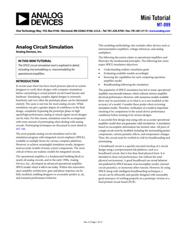
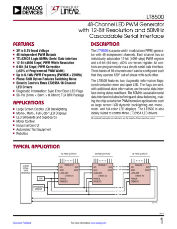
LT850048-Channel LED PWM Generatorwith 12-Bit Resolution and 50MHzCascadable Serial InterfaceFEATURESnnnnnnnnnnDESCRIPTION3V to 5.5V Input Voltage48 Independent PWM OutputsTTL/CMOS Logic 50MHz Serial Data Interface12-Bit (4096 Steps) PWM Width Resolution6-Bit (64 Steps) PWM Correction( 50% of Programmed PWM Width)Up to 6.1kHz PWM Frequency (PWMCK 25MHz)Phase-Shift Option Reduces Switching NoiseDirectly Controls Three LT3595A 16-ChannelLED DriversDiagnostic Information: Sync Error/Open LED Flags56-Pin (6mm 6mm 0.78mm) TLA QFN PackageAPPLICATIONSnnnnnnnLarge Screen Display LED BacklightingMono-, Multi-, Full-Color LED DisplaysLED Billboards and SignboardsMotor ControlIndustrial ControlAutomated Test EquipmentRoboticsThe LT 8500 is a pulse width modulation (PWM) generator with 48 independent channels. Each channel has anindividually adjustable 12-bit (4096-step) PWM registerand a 6-bit (64-step) 50% correction register. All controls are programmable via a simple serial data interface.Three banks of 16-channels each can be configured suchthat they operate 120 out-of-phase with each other.The LT8500 features two diagnostic information flags:synchronization error and open LED. The flags are sent,with additional state information, on the serial data interface during status read back. The 50MHz cascadable serialdata interface includes buffering and skew-balancing, making the chip suitable for PWM intensive applications suchas large screen LCD dynamic backlighting and mono-,multi- and full-color LED displays. The LT8500 is alsoideally suited to control three LT3595A LED drivers.All registered trademarks and trademarks are the property of their respective owners.TYPICAL APPLICATION5-WIRESERIALDATAINTERFACEOSC48 PWM OUTPUTS48 PWM OUTPUTS48 PWM OUTPUTS PWM[48:1]SDISDOSCKISCK0LDIBLANKLT8500 00 (2)PWMCKOPENLEDDIAGNOSTICCIRCUIT PWM[48:1]SDISDOSCKISCK0LDIBLANKLT8500 (N)PWMCKOPENLED 8500 TA01aRev CDocument FeedbackFor more information www.analog.com1
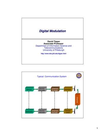
LT8500PIN CONFIGURATION(Note WM5PWM8SDISDKOSCKIOPENLEDPWM35PWM45A11 A12 A13 A14 A15 A16 A17 A18 A19 A20 13A1 A40 A39 A38 A37 A36 A35 A34 A33 A32 A31PWM2PWM24PWM4PWM3TOP VIEWPWM37VCC. –0.3V to 6VSDI, SCKI, PWMCK, OPENLED,LDIBLANK. –0.3V to Lesser of 6V and (VCC 0.3V)Operating Junction Temperature Range(Note 2). –40 C to 125 CStorage Temperature Range. –65 C to 150 CPWM44ABSOLUTE MAXIMUM RATINGSTJ PACKAGE56-LEAD PLASTIC TLA QFN (6mm 6mm)TJMAX 125 C, θJA 35 C/W, θJC 5 C/WEXPOSED PAD (PIN 57) IS GND, MUST BE SOLDERED TO PCBORDER INFORMATIONLEAD FREE FINISHTAPE AND REELPART MARKING*PACKAGE DESCRIPTIONTEMPERATURE RANGELT8500ETJ#PBFLT8500ETJ#TRPBFLT8500TJ56-Lead (6mm 6mm) Plastic TLAQFN–40 C to 125 CLT8500ITJ#PBFLT8500ITJ#TRPBFLT8500TJ56-Lead (6mm 6mm) Plastic TLAQFN–40 C to 125 CConsult ADI Marketing for parts specified with wider operating temperature ranges. *The temperature grade is identified by a label on the shipping container.Tape and reel specifications. Some packages are available in 500 unit reels through designated sales channels with #TRMPBF suffix.Rev C2For more information www.analog.com
LT8500ELECTRICAL CHARACTERISTICSThe l denotes the specifications which apply over the full operatingtemperature range, otherwise specifications are at TA 25 C. VCC 3.3V, unless otherwise VCCVCC Operating Voltagel3.0llll4.02.75.5V1.00.6VVVVDigital Inputs: SCKI, SDI, LDIBLANK, OPENLED, PWMCKVIHInput Logic LevelsHigh Level VoltageVILLow Level VoltageVCC 5VVCC 3.3VVCC 5VVCC 3.3VIINInput CurrentPin Voltage VCC or GND Excluding OPENLED–1RPUOPENLED Pull-Up ResistorVCC 5.5V70CINInput Capacitance (Note 4)Pin to GND1001µA130kΩ3pFDigital Outputs: SCKO, SDO, PWM[48:1]VOHVOLVOHVOLSDO, SCKO Output VoltagesHigh Level VoltageLow Level VoltagePWM [48:1] Output VoltagesHigh Level VoltageLow Level VoltageIOUT –6mA, VCC 5VIOUT –3mA, VCC 3.3VIOUT 6mA, VCC 5VIOUT 3mA, VCC 3.3Vllll4.02.7IOUT –3mA, VCC 5VIOUT –1.5mA, VCC 3.3VIOUT 3mA, VCC 5VIOUT 1.5mA, VCC 3.3Vllll4.02.71.00.6VVVV1.00.6VVVVTIMING CHARACTERISTICSThe l denotes the specifications which apply over the full operating temperaturerange, otherwise specifications are at TA 25 C. VCC 3.3V, and all inputs are rail-to-rail unless otherwise ata Shift Clock FrequencySCKI – SCKI (Figure 4)l50MHzfPWMCKPWMCK Clock FrequencyPWMCK – PWMCK (Figure 5)l25MHztWH-SCKIMinimum SCKI High Time (Note 3)SCKI HightWL-SCKIMinimum SCKI Low Time (Note 3)SCKI LowtWH-LDILDIBLANK Pulse Duration(LDI Function)LDIBLANK High (Figure 4)l8tWH-BLANKLDIBLANK Pulse Duration(BLANK Function)LDIBLANK High (Figure 4)l50,000nstSU-SDISDI-SCKI Setup Time (Note 3)SDI – SCKI (Figure 4)l3nstHD-SDISCKI-SDI Hold Time (Note 3)SCKI – SDI (Figure 4)l1.75nstSU-LDISCKI-LDIBLANK Setup Time (Note 3)SCKI – LDIBLANK (Figure 4)SCKI 50% Duty Cyclel10nstHD-LDILDIBLANK-SCKI Hold Time (Note 3)LDIBLANK – SCKI (Figure 4)l5tPD-SDOSCKI-SDO Propagation Delay (Note 3)SCKI – SDO (Figure 4)l1525nstPD-SCKSCKI-SCKO Propagation Delay (Note 3)SCKI – SCKO (Figure 4)l1020nstHD-SDOSCKO-SDO Hold Time (Note 3)SCKO – SDO (Figure 4)l2ns22.75ns5,000nsnsnsRev CFor more information www.analog.com3
LT8500TIMING CHARACTERISTICSThe l denotes the specifications which apply over the full operating temperaturerange, otherwise specifications are at TA 25 C. VCC 3.3V, and all inputs are rail-to-rail unless otherwise noted.SYMBOLPARAMETERCONDITIONSMINtDC-SCKSCKI-SCKO Duty Cycle Change (Note 4)Difference Between SCKI High Timeand SCKO High Time, CLOAD 25pFtPD-PWMPWMCK-PWM[48:1] Propagation Delay(Note 3)PWMCK – PWM (Figure 5)TYPMAXUNIT–0.2l32ns50nstR-SDOSDO, SCKO Rise Time (Note 4)CLOAD 25pF, 30% to 70%2nstF-SDOSDO, SCKO Fall Time (Note 4)CLOAD 25pF, 70% to 30%2nstR-PWMPWM[48:1] Rise Time (Note 4)CLOAD 25pF, 30% to 70%12nstF-PWMPWM[48:1] Fall Time (Note 4)CLOAD 25pF, 70% to 30%12nsNote 1: Stresses beyond those listed under Absolute Maximum Ratingsmay cause permanent damage to the device. Exposure to any AbsoluteMaximum Rating condition for extended periods may affect devicereliability and lifetime.Note 2: The LT8500E is guaranteed to meet performance specificationsfrom 0 C to 125 C junction temperature. Specifications over the –40 Cto 125 C operating junction temperature range are assured by design,characterization and correlation with statistical process controls. TheLT8500I is guaranteed over the full –40 C to 125 C operating junctiontemperature range.Note 3: Propagation delays, setup/hold times and hi times are measuredfrom 50% to 50%.Note 4: This parameter is correlated to lab measurements and is notsubject to production testing.Rev C4For more information www.analog.com
LT8500TIMING tHD-LDItWL-SCKISCKISDILDIBLANKSCKOSDO8500 TD01tPD-SDOtPD-SCKtHD-SDORev CFor more information www.analog.com5
LT8500TYPICAL PERFORMANCE CHARACTERISTICSFor the ICC vs VCC Graphs, the Following ConditionsApply: 23pF Load on SCKO. PWM Outputs Enabled: Duty Cycle 1365/4096, 10pF Average Load on PWMs.ICC vs VCC, SCKI 0MHz,SDI 0MHz, PWMCK 10MHzICC vs VCC, SCKI 0MHz,SDI 0MHz, PWMCK 25MHz3.03.02.52.52.52.02.02.01.5ICC (mA)3.0ICC (mA)1.51.51.01.01.00.50.50.50343.54.5VCC (V)505.53.548500 G014.5VCC (V)505.530252525202020ICC (mA)3015101055543.5VOL (V)0.64.5VCC (V)505.533.58500 G0444.5VCC (V)VOL vs VCC50.50.50.40.40.30.2PWMs AT 3mASCKO, SDO AT 6mAPWMs AT 1.8mA0.100123VCC (V)564.5VCC (V)55.58500 G0333.544.5VCC (V)55.58500 G06VOH vs VCC0.30.2PWMs AT 3mASCKO, SDO AT 6mAPWMs AT 1.8mA0.1405.58500 G050.6VCC – VOH (V)34151003.5ICC vs VCC, SCKI 50MHz,SDI 25MHz, PWMCK 25MHz301538500 G02ICC vs VCC, SCKI 20MHz,SDI 10MHz, PWMCK 10MHzICC vs VCC, SCKI 12MHz,SDI 6MHz, PWMCK 0MHzICC (mA)3ICC (mA)ICC (mA)ICC vs VCC, SCKI 0MHz,SDI 0MHz, PWMCK 0MHz008500 G07123VCC (V)4568500 G08Rev C6For more information www.analog.com
LT8500PIN FUNCTIONSPWM[48:1] (Pins A1 to A24, A29 to A40, B1 to B10,B15 to B16): Pulse Width Modulated (PWM) OutputPins. Pulse width is determined by comparing the valuein the PWMRSYNC latches to an internal PWMCK counter.Outputs are high when the value in the PWMCK counteris less than the value in PWMRSYNC[n]. The PWM frequency is determined by the signal applied to the PWMCKpin.OPENLED (Pin B11): Not Open LED Input Pin. This inputpasses diagnostic information to the host via the statusframe. When used with LT3595A LED drivers, it connectsto the wired-OR (open collector) OPENLED outputs whichindicate an open in one or more of the LED strings. Theuser can run a self test on the LT8500 to detect whichPWM output is associated with an open LED string, orother fault. This pin has an internal 100kΩ pull-up to theVCC supply rail.SDO (Pin A25): Serial Data Output Pin. This pin is theoutput of the shift register (SR), and cascades data todownstream chips or returns data to the host.SCKI (Pin B12): Serial Clock Input Pin. This clock pinprovides timing for the serial interface and the calculationof PWM values in the correction multiplier. This clock isindependent of PWMCK.VCC (Pin A26): Supply Pin. 3.0V to 5.5V. Must be locallybypassed with a capacitor to ground.SCKO (Pin B13): Serial Clock Output Pin. Buffered passthrough of SCKI. This pin cascades the clock to the nextchip or to the host.PWMCK (Pin A27): PWM Clock Input Pin. This pin provides PWM timing for the outputs. Each PWM signal isgenerated by counting the pulses on this clock from zeroto the calculated value in the PWM synchronization register (PWMRSYNC). This clock is independent of SCKI.SDI (Pin B14): Serial Data Input Pin. This pin providesserial interface data to issue commands and set up theindividual PWM channels.LDIBLANK (Pin A28): Latch Data In/Blank Input Pin. Thisis a dual function pin.LDI Function: The internal LDI signal is directly connected to the LDIBLANK pin. A logic high on the pinalways asserts the LDI function. The rising edge ofLDIBLANK captures the decoded command field(CMD, CR[7:0]) of the shift register (SR[7:0]). Thehigh level of LDIBLANK latches data from the correction multiplier into the PWM Registers (PWMR).When LDIBLANK is high, status information is loadedinto the shift register (SR) to shift out on SDO whenthe next frame shifts in on SDI. See more details inthe Operation section.BLANK Function: Asserting LDIBLANK high for morethan 50µs turns off all PWM[48:1] outputs and resetsthe chip. To avoid inadvertently resetting the chip, donot assert LDIBLANK high for more than 5µs.GND (Exposed Pad Pin 57): This is the ground referencefor the chip.Rev CFor more information www.analog.com7
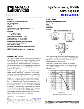
LT8500BLOCK DIAGRAMA26B11B14B12VCCOPENLED100kCRD, PHS, SYC,OLT, CR[4:7]*SDISDLDSCKISTATUS (COR’s, OLED’s)PDSHIFT REGISTER (SR[0:583])*CR[0:7]*SDOPORA25FRAME DATA (SR[8:583])*8288 {SR[14:19], SR[26, 31],., SR[578:583]}*6A28LDIBLANKLDCTRLCOR[n]6A27 48288PWMCKSEL CORRECTIONMULTIPLIERLD576SCKOPWM CHANNEL12ENPWMR[n]12EN PWMRSYNC[n]57B13PWMxx1212-BIT PWMGENERATIONGND 48PWMCKCOUNTER*REVERSE INDEXING IS USED TO INDICATE PHYSICAL BIT ORDER.8500 BDFigure 1. Block DiagramRev C8For more information www.analog.com
LT8500OPERATIONOVERVIEWThe LT8500 controls 48 pulse width modulated(PWM[48:1]) outputs, suitable for control applicationssuch as driving three LT3595A LED drivers. The chip’soperation is best understood by referring to the BlockDiagram in Figure 1.The major blocks inside the LT8500 are: a 584-bitshift register (SR[0:583]), 48 6-bit correction registers(COR[1:48]), a correction multiplier, 48 PWM channelsand a PWMCK clock counter. Each PWM channel storesdata for the associated PWMx output pin and includes aPWM register (PWMR) and a PWM synchronization register (PWMRSYNC). The lower 8 bits of the 584-bit shiftregister are the command register (CR[0:7]) and the restof the shift register contains the frame data.A comparison of a channel’s PWMRSYNC register to thePWMCK counter generates the respective PWM outputsignal. The input of the 584-bit shift register (SR[0]) isconnected to the SDI signal. SDI is also an input to thecorrection multiplier. The output of the 584-bit shift register (SR[583]) is connected to SDO.The user communicates with the part by controlling theserial interface pins SDI, SCKI and LDIBLANK. A serialdata frame, called a command frame, is shifted into thepart on SDI using SCKI as the clock signal. At the sametime, the status frame is shifted out on SDO. A rising edgeon the LDIBLANK pin terminates a frame. A frame consists of a 12-bit data field for each PWM channel, followedby an 8-bit command field, totaling (12 48) 8 584bits. The data is transmitted with the most significantchannel first, and each field is transmitted MSB first.The frame formats and timing are illustrated in Figure 3and Figure 4, respectively. There are eight commands,two of which update the PWM[48:1] outputs. The commands are summarized in Table 2. Within this document,command frames will be referred to by the commandsthey issue, such as “update frame” or “correction frame.”With a 50MHz SCKI, a single frame can be transmitted in11.7µs (584 SCKIs LDI), for a frame rate of 85.5kHz.A 25MHz PWMCK creates a PWM period (4096 PWMCKs)of 164µs, or a PWM output frequency of 6.1kHz.Update frames are used to serially load the 12-bit valuesfor each of the 48 PWM channels. The LT8500 containsa correction multiplier that can automatically scale the12-bit PWM channel data before it’s stored. By default,the correction multiplier is enabled and scales incomingchannel data according to: 2 COR n 32 PWMOUTn CHANn(NOM) 3 64 where PWMOUTn is the number of PWMCK cycles thatPWMn is high, CHANn(NOM) is the nth channel field inthe frame, and CORn is the nth programmed correctionsetting (CORn 0 to 63). See Table 1 for examples.Otherwise, when the correction multiplier is disabled, theincoming data is stored unchanged:PWMOUTn CHANn(NOM)The correction multiplier is disabled by the correction register disable bit (CRD), which is toggled by the correctiontoggle command (CMD 0x7X). By default, the correctionmultiplier is enabled after power-up and the CRD bit is low.The result generated by the correction multiplier movesto the respective PWMRSYNC register after an updateframe. An update frame does this either synchronouslyor asynchronously. A synchronous update frame will copythe data to the PWMR on the subsequent rising edge ofLDI which marks the end of the frame, and then from thePWMR to the PWMRSYNC register at the beginning of aPWM period. A PWM period starts when the free-runningPWMCK counter is zero. Otherwise, the asynchronousupdate frame will copy the data from the correction multiplier, through the PWMR to the PWMRSYNC at the sametime, on the subsequent rising edge of LDI which marksthe end of the frame.As soon as the PWMRSYNC registers are updated withtheir new values, the PWM outputs will reflect the update.As mentioned earlier, the PWMR outputs are generatedby comparing the respective PWMRSYNC values to thePWMCK counter.Rev CFor more information www.analog.com9
LT8500OPERATIONSTART-UPSERIAL DATA INTERFACEThe LT8500 is ready to communicate after power-up, ifthe LDIBLANK pin is low. The PWM[48:1] outputs remaindisabled (logic 0) until an output enable frame is sent. Therecommended sequence of events for start-up is:The LT8500 has a 50MHz cascadable serial data interfacewith full buffering and skew balancing on clock and data.The interface uses a novel 5-wire (LDIBLANK, SCKI, SDI,SCKO, and SDO) topology and can be connected to avariety of digital controllers, such as microcontrollers,digital signal processors (DSPs), or field programmablegate arrays (FPGAs).1. Apply power and drive LDIBLANK low. SDO will go lowwhen the on-chip power-on-reset (POR) de-asserts.2. Send a correction register frame (CMD 0x20) onthe serial interface. This sets the correction factor oneach channel.3. Send an update frame (CMD 0x00 or CMD 0x10)on the serial interface. This sets the pulse width ofeach channel.4. Send an output enable frame (CMD 0x30) on theserial interface. This enables the modulated pulses onthe PWM[48:1] outputs.The PWM clock (PWMCK) should be turned on beforestep 4. The start of a PWM period, when all PWM[48:1]channels turn on, is synchronized to the output enableframe when the outputs are disabled prior to the frame.TopologyTwo topologies shown in Figure 2 are supported for cascading the LT8500. For higher speeds and a large number of LT8500s, consider the novel 5-wire topology. Forlower speeds and few LT8500s, consider the conventional4-wire topology. Whichever topology is used, signal integrity should be carefully evaluated, especially for the clocks.The 5-wire topology eliminates the need for global SCKIrouting and reduces the need for buffer insertion for theSCKI signal. Instead, it provides the SCKO signal alongwith the SDO signal to drive the next chip. The skew insidethe chip between the SCKI and SDI signals is balancedinternally. The skew outside the chip between the SCKOand SDO signals can be easily balanced by parallel routingNovel 5-Wire T8500 (1)LDISCKISCK0SDISDOLT8500 (2)LDISCKISCK0SDISDOLT8500 (N)SDOSCKOConventional 4-Wire 0 (1)LDISCKISDISDOLT8500 (2)SDOLDISCKISDISDOLT8500 (N)8500 F02Figure 2. Serial Interface TopologiesRev C10For more information www.analog.com
COR 48, 6 BITSMSBMSBCOR FRAMESTATUS FRAMELSBLSB0X0XPWM 48, 12 BITS0XCOMMAND REGISTER (CR):SEE TABLE 2 FOR COMMAND REGISTER DECODING.COR 48, 6 BITSMSBUPDATE FRAME0XFor more information www.analog.comNOL48XMSBMSBMSBLSBLSBSTATUS FRAME:NOL48-NOL1:CR[7:4]:OLT:SYC:PHS:CRD:COR 1, 6 BITSCOR 1, 6 BITS0X0X0X0XNOL1XCR[7:4]MSBLSB MSBLSBLSB8500 F03OLT SYC PHS CRDCR, 8 BITSCR, 8 BITSFAULT 0, OK 1LAST COMMANDOPENLED TESTED 1, OPENLED NOT TESTED 0OUT-OF-SYNC 1, OK 0PHASE-SHIFTED 1, NOT SHIFTED 0CORRECTION DISABLED 1, CORRECTION ENABLED 00XPWM 1, 12 BITSFigure 3. Serial Data Frame Format0XLSB584 BITSLT8500OPERATIONRev C11
12For more information COR 48MSBCOR 48MSBCOR 48MSB-14CR2DC 48MSB-3CR0CR1CR1582tHD-SDICOR 48MSB-4COR 48MSB-5tSU-SDI583CR1CR0PHSCRDPWM 48MSBPWM 48MSB-10tHD-SDOtPD-SDOtPD-SCK4COR 48MSB(PRIOR)STATUS DATACOR 48MSB (NEW)5830COR 48MSB-1(PRIOR)Figure 4. Serial Data Input and Output Timing ChartINPUT DATA582CR2CR1582CR0CRD582AFTER A CORRECTION FRAME (CMD 0x2X)CRDPWM 48MSB0ALL PWM REGISTERS ARE UPDATED FROM CORRECTION MULTIPLIER ON LDI AFTER AN UPDATE FRAME (CMD 0x2X or 0x1X)ALL CORRECTION REGISTERS UPDATED FROM SHIFT REGISTER ON LDI01/fSCK1tWL-SCKI tWH-SCKI tSU-LDI tWH-LDI tHD-LDIPWM 48MSB583CR1CR0583PHSCRD8500 F04COR 48MSB (NEW)XLT8500OPERATIONRev C
LT8500OPERATIONthese two signals between chips. When properly balancedin this way, the SCKO/SDO timing will meet the timingrequirements of SCKI/SDI on the next cascaded chip,enabling faster clock speeds and more chips in cascade.The host controller sends the SDI signal with the SCKIsignal, and receives the SDO signal with the SCKO signal.The controller will see skew between SCKI and SCKO,and will need to operate on two clock planes dependingon the number of cascaded LT8500s and system timingconstraints. A duty cycle change (tDC-SCK ) will also occurbetween SCKI and SCKO, limiting the number of LT8500sin a chain, depending on SCKI speed. This change resultsfrom a slight difference in propagation delays of the positive and negative edges of SCKI. LDIBLANK skew betweenchips may require balancing in timing critical systems,otherwise the host should increase the delay betweenSCKI and LDI to avoid violating LDI to SCKI setup andhold times (tSU-LDI and tHD-LDI). In summary, the 5-wiretopology extends the maximum number of cascadablechips, boosts the series data interface clock frequency,eliminates global SCKI routing, reduces the need of buffer insertion for SCKI signals, and offers an easier PCBlayout. In a low-speed application with a small number ofcascaded chips, the 5-wire topology can be simplified tothe 4-wire topology by ignoring the SCKO output.In a 4-wire topology, the LDIBLANK and SCKI signalsneed global routing while the SDI signal only needs localrouting between chips. SCKO is ignored. When a largenumber of chips are in cascade, or long board tracesare used, external clock-tree buffers with correspondingdriving capability might be needed for the LDIBLANK andSCKI signals to minimize signal skews. The propagationdelay caused by the buffer insertion on the SCKI signalyields the skew between the SCKI and SDI signals, whichusually requires balancing. Since both the SDI and SDOsignals require the same SCKI signal to send and receive,the propagation delay between the SDI and SDO signalslimits the number of chips in cascade and the series datainterface clock frequency.CommunicationFigure 3 shows two command frames sent on SDI, andone status frame received on SDO. All the frames havethe same 584-bit length and are transmitted with the mostsignificant channel first, and each field is transmitted withMSB first. The command frames are sent with the SCKIsignal and the status frame is received with the SCKOsignal. The command field determines the function of aframe, according to Table 2. The status frame consists ofthe four MSB’s of the last command (CR[7:4]), the openLED self test bit (OLT), the synchronization error statusbit (SYC), the phase-shift status bit (PHS), the correctionregister disable status bit (CRD), and individual OPENLEDfault bits (NOL[48:1]), as well as each 6-bit correctionregister (COR[48:1]). Logic zeros fill in the unused bitsof the status frame. Refer to Figure 3.Figure 4 illustrates the timing relationship among serialinput and serial output signals in more detail. One correction register frame followed by an update frame is sentthrough the SDI, SCKI, and LDIBLANK pins. At the sametime, two status frames are received through the SDO,SCKO, and LDIBLANK pins. The rising edges of SCKI shifta frame of data into shift register SR[0:583]. After 584clock cycles, all bits of data sit in the shift register waitingfor the LDI signal. An asynchronous LDIBLANK “high”signal captures the decoded 8-bit CMD field (CR[7:0]),executing commands and routing data accordingly. Atthe same time, a frame of status information, includingthe 4 MSB’s of the CMD field (CR[7:4]), status bits, CORregisters, and individual open LED fault flags, is parallelloaded into the 584-bit shift register and will be shiftedout as the next frame shifts in.LDIBLANK LDI BLANKThe LDIBLANK pin is a dual function input, determined bythe duration of a logic high on the pin. LDI is the latch datainput, which signals the end of a frame and executes thecommand in the CMD field (CR[7:0]). The BLANK signalturns off the PWM[48:1] outputs and performs a globalreset of the part, including the shift register in the serialinterface. A logic high on LDIBLANK always asserts LDI,while a logic high greater than the minimum LDIBLANKpulse duration for BLANK (tWH-BLANK) also asserts BLANK.BLANK will never be asserted if the pin is held high less thanthe maximum LDIBLANK pulse duration for LDI (tWH-LDI).Between maximum tWH-LDI and minimum tWH-BLANK,BLANK becomes asserted at an undetermined time.Rev CFor more information www.analog.com13
LT8500OPERATIONA rising edge on the LDI signal is always interpreted asthe end of a frame. The next rising edge of SCKI after thefalling edge of LDIBLANK is always interpreted as the startof a new frame. An out-of-sync error bit (SYC) is providedin the status frame to alert the system if the part saw anLDI unexpectedly. This occurs when LDI and SCKI areboth hi, or when LDI is hi on other than a frame boundary(n 584 SCKI’s). The SYC bit is for information only, it hasno other effect on the part. If the SYC bit is set, none ofthe other data in the status frame is reliable and the effectof the prior frame is unknown; the LT8500 assumes thesystem’s timing of the LDI is correct and considers thenext SCKI as the start of the next frame.OPENLEDThe OPENLED pin provides status information to the hostby reporting its state in the status frame. The state ofthe pin is captured by each rising edge of PWMCK andis reported in two ways. In typical use, the status framereceives the captured state of the pin on the rising edgeof the first SCKI after LDIBLANK goes low. This state isduplicated 48 times and reported in the LSB of each PWMchannel in the status frame. The state will normally be alogic “1” due to the on-chip pull-up resistor.Alternatively, the LT8500 supports a diagnostic self testframe (CMD 0x5X) that reports the OPENLED state differently. In this case, the LT8500 sequentially pulsesPWM[1] through PWM[48] high for 64 PWMCK cycleseach. The state of the OPENLED pin is captured for eachchannel while the corresponding PWM pin is high. This bychannel data is shifted out in the status frame as the nextframe is shifted in. In addition, the status frame will setthe open LED test bit (OLT), indicating that the OPENLEDdata in the current status frame is from the self test. Thestatus frame will return to typical reporting on the following frame. When the LT8500 is used with the LT3595A, theOPENLED pin and the self test provide a diagnostic routineto identify the location of open LED faults. See “DiagnosticInformation Flags” in the Applications Information section.OUTPUTSAfter power-up or reset, no PWM[48:1] output will turn onuntil an output enable frame is sent. The 12-bit PWMCKcounter is free-running from the PWMCK clock whenoutputs are enabled. When an output enable frame is sent,the PWMCK counter increments to one on the second rising edge of PWMCK after the rising edge of LDIBLANK,as shown in Figure 5. By default, all outputs with nonzero values in PWMRSYNC will turn on when the PWMCKcounter is one. Alternatively, if the phase-shift bit (PHS)is set, the PWM[48:1] outputs will turn on as illustrated inthe phase-shift synchronous updates in Figure 6, case A.Further discussion of the phase-shift function follows.Each subsequent rising edge of PWMCK increases thePWMCK counter by one. Any PWM channel will be turnedoff when its PWMRSYNC value is equal to the value inthe PWMCK counter. An output disable frame resets thePWMCK counter immediately after LDI, and turns off allthe PWM channels on the next rising edge of PWMCK afterLDI. Figure 5 shows the PWM output enable timing chart.1fPWMCKPWMCKtPD-PWM0123LDI, CMD 0x308500 F05PWMFigure 5. PWM Output Enable Timing ChartAssumes Outputs Were Previously DisabledPHASE DIFFERENCE BETWEEN 16-CHANNEL BANKSBy default, the rising edges of all PWM[48:1] channelsoccur on the same rising edge of PWMCK. This eventbegins a PWM period of 4096 PWMCK cycles. TheLT8500 provides a phase-shift toggle command (CMD 0x6X) to reduce system noise and current spikes resulting from 48 pins switching at once. The function of thiscommand is illustrated in Figure 6, case A. In phase-shiftmode, the PWM[48:1] outputs are divided into three16-channel banks that are 120 degrees out-of-phasewith each other within a PWM period. This means thatchannels PWM[48:33] will turn on with the rising edge ofPWMCK(1), then channels PWM[32:17] will turn on withthe rising edge of PWMCK(1365), 1/3 of the PWM period,and channels PWM[16:1] will turn on with the rising edgeof PWMCK(2730), 2/3 of the PWM period.Rev C14For more information www.analog.com
LT8500OPERATIONTable 1. Example PWM Width Calculations (Base 10) with Correction Enabled (CRD 0)APWM UPDATE VALUESENT ON SDIBPRESCALED PWM(A 2/3)CCORRECTION REGISTER(COR) VALUEDMULTIPLIER(C 32)/64EPWM WIDTH (B D)(IN UNITS OF 4095273000.51365PWM CALCULATION BY DIGITAL MULTIPLICATION OFCORRECTION REGISTER AND PWM UPDATE VALUESThe correction multiplier is used to automatically scalethe 12-bit PWM channel data before storing the PWMupdate value for the respective channel. The correctionmultiplier is disabled by the correction register disablebit (CRD), which is toggled by the correction toggle command (CMD 0x7X). When the correction multiplier is disabled, the incoming data is stored unchanged:PWMOUTn CHANn(NOM)The correction multiplier is enabled by default (CRD 0)and scales incoming channel data according to: 2 DCRn 32 GSRn(CALC) GSRn (NOM) 3 64where PWMOUTn is the number of PWMCK cycles thatPWMn is high, CHANn(NOM) is the nth channel field inthe frame, and CORn is the nth programmed correctionsetting (CORn 0 to 63). See Table 1 for examples.The 6-bit COR value sets a multiplier of 0.5X to 1.5X(exactly 1.484375, or ((63 32)/64)) with 64 values anda midrange, signifying a multiple of 1.0, at 32 (0x20).In order to avoid overflow in the PWM registers whenthe multiplier is greater than 1.0, the nominal PWMupdate value (CHANn) is first prescaled on chip by 2/3.This means that the full-scale width for a channel with amultiplier of 1.0 (CHANn 4095, CORn 32) will resultin a PWMOUTn width of 4095 (2/3) 1.0 2730, not4095. So, a correction multiplier of 1.5 (CORn 63)yields a corrected PWM width of 4052 4095 (2/3) 1.484375. The P
LT8500 6 Re C For more information www.analog.com TYPICAL PERFORMANCE CHARACTERISTICS ICC vs VCC, SCKI 12MHz, SDI 6MHz, PWMCK 0MHz ICC vs VCC, SCKI 20MHz, SDI 10MHz, PWMCK 10MHz ICC vs VCC, SCKI 50MHz, SDI 25MHz, PWMCK 25MHz