Transcription
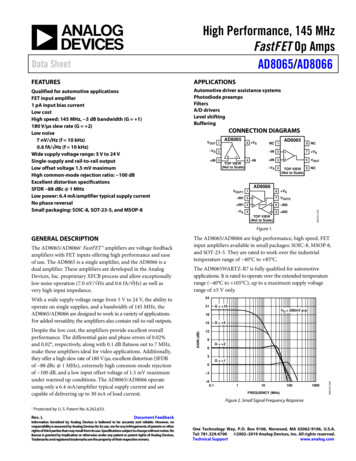
High Performance, 145 MHzFastFET Op AmpsAD8065/AD8066Data SheetFEATURESAPPLICATIONSQualified for automotive applicationsFET input amplifier1 pA input bias currentLow costHigh speed: 145 MHz, 3 dB bandwidth (G 1)180 V/µs slew rate (G 2)Low noise7 nV/ Hz (f 10 kHz)0.6 fA/ Hz (f 10 kHz)Wide supply voltage range: 5 V to 24 VSingle-supply and rail-to-rail outputLow offset voltage 1.5 mV maximumHigh common-mode rejection ratio: 100 dBExcellent distortion specificationsSFDR 88 dBc @ 1 MHzLow power: 6.4 mA/amplifier typical supply currentNo phase reversalSmall packaging: SOIC-8, SOT-23-5, and MSOP-8Automotive driver assistance systemsPhotodiode preampsFiltersA/D driversLevel shiftingBufferingCONNECTION DIAGRAMSVOUT 1AD80655 VSNC 1–VS 2 IN 3AD8065–IN 2TOP VIEW(Not to Scale)4 –IN8 NC7 VS IN 36VOUT–VS 45NCTOP VIEW(Not to Scale)8 VS–IN1 27VOUT2 IN1 36–IN2–VS 45 IN2TOP VIEW(Not to Scale)02916-E-001AD8066VOUT1 1Figure 1.The AD8065/AD8066 FastFET amplifiers are voltage feedbackamplifiers with FET inputs offering high performance and easeof use. The AD8065 is a single amplifier, and the AD8066 is adual amplifier. These amplifiers are developed in the AnalogDevices, Inc. proprietary XFCB process and allow exceptionallylow noise operation (7.0 nV/ Hz and 0.6 fA/ Hz) as well asvery high input impedance.1The AD8065/AD8066 are high performance, high speed, FETinput amplifiers available in small packages: SOIC-8, MSOP-8,and SOT-23-5. They are rated to work over the industrialtemperature range of 40 C to 85 C.The AD8065WARTZ-R7 is fully qualified for automotiveapplications. It is rated to operate over the extended temperaturerange ( 40 C to 105 C), up to a maximum supply voltagerange of 5 V only.With a wide supply voltage range from 5 V to 24 V, the ability tooperate on single supplies, and a bandwidth of 145 MHz, theAD8065/AD8066 are designed to work in a variety of applications.For added versatility, the amplifiers also contain rail-to-rail outputs.21G 10VO 200mV p-p1815GAIN (dB)Despite the low cost, the amplifiers provide excellent overallperformance. The differential gain and phase errors of 0.02%and 0.02 , respectively, along with 0.1 dB flatness out to 7 MHz,make these amplifiers ideal for video applications. Additionally,they offer a high slew rate of 180 V/µs, excellent distortion (SFDRof 88 dBc @ 1 MHz), extremely high common-mode rejectionof 100 dB, and a low input offset voltage of 1.5 mV maximumunder warmed up conditions. The AD8065/AD8066 operateusing only a 6.4 mA/amplifier typical supply current and arecapable of delivering up to 30 mA of load current.24G 5129G 263G 10–3–60.1110100FREQUENCY (MHz)100002916-E-002GENERAL DESCRIPTIONFigure 2. Small Signal Frequency Response1Protected by U. S. Patent No. 6,262,633.Rev. LDocument FeedbackInformation furnished by Analog Devices is believed to be accurate and reliable. However, noresponsibility is assumed by Analog Devices for its use, nor for any infringements of patents or otherrights of third parties that may result from its use. Specifications subject to change without notice. Nolicense is granted by implication or otherwise under any patent or patent rights of Analog Devices.Trademarks and registered trademarks are the property of their respective owners.One Technology Way, P.O. Box 9106, Norwood, MA 02062-9106, U.S.A.Tel: 781.329.4700 2002–2019 Analog Devices, Inc. All rights reserved.Technical Supportwww.analog.com
AD8065/AD8066Data SheetTABLE OF CONTENTSFeatures . 1Wideband Operation . 21Applications . 1Input Protection . 21Connection Diagrams . 1Thermal Considerations. 22General Description . 1Input and Output Overload Behavior . 22Revision History . 3Layout, Grounding, and Bypassing Considerations . 23Specifications 5 V . 4Power Supply Bypassing . 23Specifications 12 V . 6Grounding . 23Specifications 5 V . 7Leakage Currents . 23Absolute Maximum Ratings . 9Input Capacitance . 23Maximum Power Dissipation . 9Output Capacitance . 23Output Short Circuit . 9Input-to-Output Coupling . 24ESD Caution . 9Wideband Photodiode Preamp . 24Typical Performance Characteristics . 10High Speed JFET Input Instrumentation Amplifier. 25Test Circuits . 17Video Buffer . 26Theory of Operation . 20Outline Dimensions . 27Closed-Loop Frequency Response . 20Ordering Guide . 28Noninverting Closed-Loop Frequency Response . 20Automotive Products . 28Inverting Closed-Loop Frequency Response . 20Rev. L Page 2 of 28
Data SheetAD8065/AD8066REVISION HISTORY1/2019—Rev. K to Rev. LChanged AD8065WARTZ-REEL7 toAD8065WARTZ-R7 . Throughout8/2016—Rev. J to Rev. KUpdated Outline Dimensions .27Changes to Ordering Guide .288/2010—Rev. I to Rev. JChanges to Features Section, Applications Section, and GeneralDescription Section . 1Change to Table 1 . 4Change to Table 3 . 7Changes to Table 4 . 9Changes to Figure 9.10Changes to Inverting Closed-Loop Frequency ResponseSection .20Moved Leakage Currents Section, Input Capacitance Section,and Output Capacitance Section .23Moved Input-to-Input Coupling Section, WidebandPhotodiode Preamp Section, and Figure 59 .24Changes to Table 5 .25Moved Figure 60 and High Speed JFET Input InstrumentationAmplifier Section .25Updated Outline Dimensions .27Changes to Ordering Guide .28Added Automotive Products Section .283/2009—Rev. H to Rev. IChanges to High Speed JFET Input Instrumentation AmplifierSection .23Updated Outline Dimensions .249/2008—Rev. G to Rev. HDeleted Usable Range Parameter, Table 1 . 3Deleted Usable Range Parameter, Table 2 . 4Deleted Usable Range Parameter, Table 3 . 5Changes to Layout . 6Changes to Input and Output Overload Behavior Section.19Changes to Table 5 Expressions Column .221/2006—Rev. F to Rev. GChanges to Ordering Guide .2612/2005—Rev. E to Rev. FUpdated Format. UniversalChanges to Features . 1Changes to General Description . 1Changes to Figure 22 through Figure 27. 11Updated Outline Dimensions. 25Changes to Ordering Guide . 262/2004—Rev. D to Rev. E.Updated Format . UniversalUpdated Figure 56 . 21Updated Outline Dimensions. 25Updated Ordering Guide . 2611/2003—Rev. C to Rev. D.Changes to Features .1Changes to Connection Diagrams .1Updated Ordering Guide .5Updated Outline Dimensions. 224/2003—Rev. B to Rev. C.Added SOIC-8 (R) for the AD8065 .42/2003—Rev. A to Rev. B.Changes to Absolute Maximum Ratings.4Changes to Test Circuit 10 . 14Changes to Test Circuit 11 . 15Changes to Noninverting Closed-Loop Frequency Response 16Changes to Inverting Closed-Loop Frequency Response . 16Updated Figure 6 . 18Changes to Figure 7 . 19Changes to Figure 10 . 21Changes to Figure 11 . 22Changes to High Speed JFET Instrumentation Amplifier . 22Changes to Video Buffer . 228/2002—Rev. 0 to Rev. A.Added AD8066 . UniversalAdded SOIC-8 (R) and MSOP-8 (RM) .1Edits to General Description .1Edits to Specifications .2New Figure 2 .5Changes to Ordering Guide .5Edits to TPCs 18, 25, and 28 .8New TPC 36 . 11Added Test Circuits 10 and 11 . 14MSOP (RM-8) Added . 23Rev. L Page 3 of 28
AD8065/AD8066Data SheetSPECIFICATIONS 5 V@ TA 25 C, VS 5 V, RL 1 kΩ, unless otherwise noted.Table 1.ParameterDYNAMIC PERFORMANCE 3 dB BandwidthBandwidth for 0.1 dB FlatnessInput Overdrive Recovery TimeOutput Recovery TimeSlew RateSettling Time to 0.1%NOISE/HARMONIC PERFORMANCESFDRThird-Order InterceptInput Voltage NoiseInput Current NoiseDifferential Gain ErrorDifferential Phase ErrorDC PERFORMANCEInput Offset VoltageConditionsMinTypG 1, VO 0.2 V p-p (AD8065)AD8065WARTZ only: TMIN TMAXG 1, VO 0.2 V p-p (AD8066)G 2, VO 0.2 V p-pG 2, VO 2 V p-pG 2, VO 0.2 V p-pG 1, 5.5 V to 5.5 VG 1, 5.5 V to 5.5 VG 2, VO 4 V stepAD8065WARTZ only: TMIN TMAXG 2, VO 2 V stepG 2, VO 8 V step1008810014555205fC 1 MHz, G 2, VO 2 V p-pfC 5 MHz, G 2, VO 2 V p-pfC 1 MHz, G 2, VO 8 V p-pfC 10 MHz, RL 100 Ωf 10 kHzf 10 kHzNTSC, G 2, RL 150 ΩNTSC, G 2, RL 150 Ω 88 67 732470.60.020.02dBcdBcdBcdBmnV/ HzfA/ Hz%DegreesVCM 0 V, SOIC packageAD8065WARTZ only: TMIN TMAX0.4130155TMIN to TMAXVO 3 V, RL 1 kΩAD8065WARTZ only: TMIN TMAXINPUT CHARACTERISTICSCommon-Mode Input ImpedanceDifferential Input ImpedanceInput Common-Mode Voltage RangeFET Input RangeCommon-Mode Rejection Ratio120504271751701801AD8065WARTZ only: TMIN TMAXSOIC packageTMIN to TMAXInput Offset CurrentOpen-Loop GainUnitMHzMHzMHzMHzMHzMHznsnsV/µsV/µsnsnsInput Offset Voltage DriftInput Bias CurrentMaxAD8065WARTZ only: TMIN TMAXVCM 1 V to 1 VVCM 1 V to 1 V (SOT-23)AD8065WARTZ only: TMIN TMAXRev. L Page 4 of 28100100 5 to 1.7 5 to 1.7 85 82 82225111131.52.61717612510125mVmVµV/ CµV/ CpApApApAdBdB1000 2.11000 4.5GΩ pFGΩ pF 5.0 to 2.4VVdBdBdB 100 91
Data SheetParameterOUTPUT CHARACTERISTICSOutput Voltage SwingOutput CurrentShort-Circuit CurrentCapacitive Load DrivePOWER SUPPLYOperating RangeAD8065/AD8066ConditionsMinTypRL 1 kΩAD8065WARTZ only: TMIN TMAXRL 150 ΩVO 9 V p-p, SFDR 60 dBc, f 500 kHz 4.88 to 4.90 4.88 to 4.90 4.94 to 4.9555Quiescent Current per AmplifierPower Supply Rejection Ratio6.4AD8065WARTZ only: TMIN TMAX PSRRAD8065WARTZ only: TMIN TMAXRev. L Page 5 of 28 85 85 100UnitVVVmAmApF 4.8 to 4.735902030% overshoot G 1AD8065WARTZ only: TMIN TMAXMax24107.27.2VVmAmAdBdB
AD8065/AD8066Data SheetSPECIFICATIONS 12 V@ TA 25 C, VS 12 V, RL 1 kΩ, unless otherwise noted.Table 2.ParameterDYNAMIC PERFORMANCE 3 dB BandwidthBandwidth for 0.1 dB FlatnessInput Overdrive RecoveryOutput Overdrive RecoverySlew RateSettling Time to 0.1%NOISE/HARMONIC PERFORMANCESFDRThird-Order InterceptInput Voltage NoiseInput Current NoiseDifferential Gain ErrorDifferential Phase ErrorDC PERFORMANCEInput Offset VoltageInput Offset Voltage DriftInput Bias CurrentConditionsMinTypG 1, VO 0.2 V p-p (AD8065)G 1, VO 0.2 V p-p (AD8066)G 2, VO 0.2 V p-pG 2, VO 2 V p-pG 2, VO 0.2 V p-pG 1, 12.5 V to 12.5 VG 1, 12.5 V to 12.5 VG 2, VO 4 V stepG 2, VO 2 V stepG 2, VO 10 V nsnsV/µsnsnsfC 1 MHz, G 2, VO 2 V p-pfC 5 MHz, G 2, VO 2 V p-pfC 1 MHz, G 2, VO 10 V p-pfC 10 MHz, RL 100 Ωf 10 kHzf 10 kHzNTSC, G 2, RL 150 ΩNTSC, G 2, RL 150 Ω 100 67 8524710.040.03dBcdBcdBcdBmnV/ HzfA/ Hz%DegreesVCM 0 V, SOIC package0.4132522114130SOIC packageTMIN to TMAXInput Offset CurrentOpen-Loop GainINPUT CHARACTERISTICSCommon-Mode Input ImpedanceDifferential Input ImpedanceInput Common-Mode Voltage RangeFET Input RangeCommon-Mode Rejection RatioOUTPUT CHARACTERISTICSOutput Voltage SwingOutput CurrentShort-Circuit CurrentCapacitive Load DrivePOWER SUPPLYOperating RangeQuiescent Current per AmplifierPower Supply Rejection RatioTMIN to TMAXVO 10 V, RL 1 kΩVCM 1 V to 1 VVCM 1 V to 1 V (SOT-23)RL 1 kΩRL 350 ΩVO 22 V p-p, SFDR 60 dBc, f 500 kHz10310mVµV/ CpApApApAdBGΩ pFGΩ pF 12 to 8.5 85 82 12.0 to 9.5 100 91VdBdB 11.8 to 11.8 11.9 to 11.9 11.25 to 11.53012025VVmAmApF5 84Rev. L Page 6 of 281.5177Unit1000 2.11000 4.530% overshoot G 1 PSRRMax6.6 93247.4VmAdB
Data SheetAD8065/AD8066SPECIFICATIONS 5 V@ TA 25 C, VS 5 V, RL 1 kΩ, unless otherwise noted.Table 3.ParameterDYNAMIC PERFORMANCE 3 dB BandwidthBandwidth for 0.1 dB FlatnessInput Overdrive Recovery TimeOutput Recovery TimeSlew RateSettling Time to 0.1%NOISE/HARMONIC PERFORMANCESFDRThird-Order InterceptInput Voltage NoiseInput Current NoiseDifferential Gain ErrorDifferential Phase ErrorDC PERFORMANCEInput Offset VoltageConditionsMinTypG 1, VO 0.2 V p-p (AD8065)AD8065WARTZ only: TMIN TMAXG 1, VO 0.2 V p-p (AD8066)G 2, VO 0.2 V p-pG 2, VO 2 V p-pG 2, VO 0.2 V p-pG 1, 0.5 V to 5.5 VG 1, 0.5 V to 5.5 VG 2, VO 2 V stepAD8065WARTZ only: TMIN TMAXG 2, VO 2 V step1259011015560fC 1 MHz, G 2, VO 2 V p-pfC 5 MHz, G 2, VO 2 V p-pfC 10 MHz, RL 100 Ωf 10 kHzf 10 kHzNTSC, G 2, RL 150 ΩNTSC, G 2, RL 150 Ω 65 502270.60.130.16dBcdBcdBmnV/ HzfA/ Hz%DegreesVCM 1.0 V, SOIC packageAD8065WARTZ only: TMIN TMAX0.4105123TMIN to TMAXVO 1 V to 4 V (AD8065)AD8065WARTZ only: TMIN TMAXVO 1 V to 4 V (AD8066)INPUT CHARACTERISTICSCommon-Mode Input ImpedanceDifferential Input ImpedanceInput Common-Mode Voltage RangeFET Input RangeCommon-Mode Rejection RatioOUTPUT CHARACTERISTICSOutput Voltage SwingOutput CurrentShort-Circuit CurrentCapacitive Load AdBdBdB1000 2.11000 4.5GΩ pFGΩ pF0 to 2.4VVdBdBdB1AD8065WARTZ only: TMIN TMAXSOIC packageTMIN to TMAXInput Offset CurrentOpen-Loop GainUnitMHzMHzMHzMHzMHzMHznsnsV/µsV/µsnsInput Offset Voltage DriftInput Bias CurrentMaxAD8065WARTZ only: TMIN TMAXVCM 0.5 V to 1.5 VVCM 1 V to 2 V (SOT-23)AD8065WARTZ only: TMIN-TMAXRL 1 kΩAD8065WARTZ only: TMIN TMAXRL 150 ΩVO 4 V p-p, SFDR 60 dBc, f 500 kHz30% overshoot G 1Rev. L Page 7 of 28100100900 to 1.70 to 1.7 74 78 760.1 to 4.850.1 to 4.8512511113 100 910.03 to 4.950.07 to 4.83357551.52.6171751255125VVVmAmApF
AD8065/AD8066ParameterPOWER SUPPLYOperating RangeData SheetConditionsMinAD8065WARTZ only: TMIN TMAX555.8Quiescent Current per AmplifierPower Supply Rejection RatioAD8065WARTZ only: TMIN TMAX PSRRAD8065WARTZ only: TMIN TMAXRev. L Page 8 of 28 78 78Typ6.4 100MaxUnit24107.07.0VVmAmAdBdB
Data SheetAD8065/AD8066ABSOLUTE MAXIMUM RATINGSRMS output voltages should be considered. If RL is referenced toVS , as in single-supply operation, then the total drive power isVS IOUT.Table 4.Rating26.4 VSee Figure 3VEE 0.5 V to VCC 0.5 V1.8 V 65 C to 125 C 40 C to 85 C 40 C to 105 C300 CIf the rms signal levels are indeterminate, then consider theworst case, when VOUT VS/4 for RL to midsupply.PD (VS I S ) (VS /4 )2RLIn single-supply operation with RL referenced to VS , worst caseis VOUT VS/2.2.0MAXIMUM POWER DISSIPATIONThe maximum safe power dissipation in the AD8065/AD8066packages is limited by the associated rise in junction temperature(TJ) on the die. The plastic encapsulating the die locally reachesthe junction temperature. At approximately 150 C, which is theglass transition temperature, the plastic changes its properties.Even temporarily exceeding this temperature limit can changethe stresses that the package exerts on the die, permanentlyshifting the parametric performance of the AD8065/AD8066.Exceeding a junction temperature of 175 C for an extendedtime can result in changes in the silicon devices, potentiallycausing failure.The still air thermal properties of the package and PCB (θJA),ambient temperature (TA), and total power dissipated in thepackage (PD) determine the junction temperature of the die.The junction temperature can be calculated 4060AMBIENT TEMPERATURE ( C)8010002916-E-003Stresses at or above those listed under Absolute MaximumRatings may cause permanent damage to the product. This is astress rating only; functional operation of the product at theseor any other conditions above those indicated in the operationalsection of this specification is not implied. Operation beyondthe maximum operating conditions for extended periods mayaffect product reliability.MAXIMUM POWER DISSIPATION (W)ParameterSupply VoltagePower DissipationCommon-Mode Input VoltageDifferential Input VoltageStorage Temperature RangeOperating Temperature RangeAD8065WARTZ OnlyLead Temperature(Soldering, 10 sec)Figure 3. Maximum Power Dissipation vs. Temperature for a 4-Layer BoardAirflow increases heat dissipation, effectively reducing θJA. Also,more metal directly in contact with the package leads frommetal traces, through holes, ground, and power planes reducethe θJA. Care must be taken to minimize parasitic capacitancesat the input leads of high speed op amps as discussed in theLayout, Grounding, and Bypassing Considerations section.Figure 3 shows the maximum safe power dissipation in thepackage vs. the ambient temperature for the SOIC (125 C/W),SOT-23 (180 C/W), and MSOP (150 C/W) packages on aJEDEC standard 4-layer board. θJA values are approximations.TJ TA (PD θJA)The power dissipated in the package (PD) is the sum of thequiescent power dissipation and the power dissipated in thepackage due to the load drive for all outputs. The quiescentpower is the voltage between the supply pins (VS) times thequiescent current (IS). Assuming the load (RL) is referenced tomidsupply, then the total drive power is VS /2 IOUT, some ofwhich is dissipated in the package and some in the load (VOUT IOUT). The difference between the total drive power and the loadpower is the drive power dissipated in the package.OUTPUT SHORT CIRCUITShorting the output to ground or drawing excessive current forthe AD8065/AD8066 will likely cause catastrophic failure.ESD CAUTIONPD Quiescent Power (Total Drive Power Load Power ) V V V OUT 2PD (VS I S ) S OUT RL RL 2Rev. L Page 9 of 28
AD8065/AD8066Data SheetTYPICAL PERFORMANCE CHARACTERISTICSDefault Conditions: 5 V, CL 5 pF, RL 1 kΩ, VOUT 2 V p-p, Temperature 25 C.246.9RL 150Ω216.8G 10G 2VO 200mV p-p18G 5VOUT 0.7V p-p6.6129G 26VOUT 1.4V p-p6.5GAIN (dB)GAIN (dB)15VOUT 0.2V p-p6.76.46.336.26.1–36.01101001000FREQUENCY (MHz)5.90.102916-E-004–60.110102916-E-007G 10100FREQUENCY (MHz)Figure 4. Small Signal Frequency Response for Various GainsFigure 7. 0.1 dB Flatness Frequency Response (See Figure 43)69VO 200mV p-pVO 200mV p-pG 1G 248VS 5VVS 5V7GAIN (dB)0VS 12V6VS 12V–25–44–60.11101001000FREQUENCY (MHz)VS 5V30.11001000FREQUENCY (MHz)Figure 5. Small Signal Frequency Response for Various Supplies(See Figure 42)Figure 8. Small Signal Frequency Response for Various Supplies(See Figure 43)82VO 2V p-p110102916-E-008VS 5V02916-E-005GAIN (dB)2G 17VO 2V p-pG 2VS 5VVS 5V60VS 12VGAIN (dB)–1VS 12V–2543–32–41101001000FREQUENCY (MHz)00.11101001000FREQUENCY (MHz)Figure 9. Large Signal Frequency Response for Various Supplies(See Figure 43)Figure 6. Large Signal Frequency Response for Various Supplies(See Figure 42)Rev. L Page 10 of 2802916-009–50.1102916-E-006GAIN (dB)VS 5V
Data SheetAD8065/AD806698VO 200mV p-pG 16CL 25pFCL 25pFRSNUB 20Ω6CL 55pFCL 5pF4CL 20pFCL 25pFGAIN (dB)GAIN (dB)30CL 5pF20–2–3–4–61101001000FREQUENCY (MHz)–80.102916-E-010–90.1Figure 10. Small Signal Frequency Response for Various CLOAD (See Figure 42)VO 200mV p-pG 21101001000FREQUENCY (MHz)02916-E-013–6Figure 13. Small Signal Frequency Response for Various CLOAD (See Figure 43)88VOUT 0.2V p-p6625VOUT 4V p-p04–23–42–61–80.100.11101001000FREQUENCY (MHz)Figure 11. Frequency Response for Various Output Amplitudes(See Figure 43)RL 1kΩVO 200mV p-pG 21100101000FREQUENCY (MHz)02916-E-014GAIN (dB)402916-E-011GAIN (dB)RL 100Ω7VOUT 2V p-pG 2Figure 14. Small Signal Frequency Response for Various RLOAD (See Figure 43)8014120VO 200mV p-pG 2GAIN (dB)8RF RG 500Ω,RS 250Ω64RF RG 1kΩ,RS 500Ω,CF 3.3pF2RF RG 500Ω,RS 250Ω,CF 2.2pF06060400GAIN20–600–120PHASE (DEGREES)PHASERF RG 1kΩ,RS 500Ω10OPEN-LOOP GAIN (dB)12110FREQUENCY (MHz)1001000Figure 12. Small Signal Frequency Response for Various RF/CF (See Figure 43)Rev. L Page 11 of 28–200.010.1110100FREQUENCY (MHz)Figure 15. Open-Loop 2
AD8065/AD8066Data Sheet–40–30–40G 2–50–50DISTORTION (dBc)–70HD2 RL 150ΩHD2 RL 1kΩ–80HD3 RL 1kΩ–90HD2 G 2HD3 G 2–70HD2 G 1–80–90HD3 RL 150ΩHD3 G 1–100–110110010FREQUENCY (MHz)–1100.102916-E-016–1200.110100FREQUENCY (MHz)Figure 19. Harmonic Distortion vs. Frequency for Various Gains(See Figure 42 and Figure 43)Figure 16. Harmonic Distortion vs. Frequency for Various Loads(See Figure 43)–20–30–40–30G 2VS 12VF 1MHz–60HD2 RL 150Ω–70HD3 RL 150Ω–80VS 12VG 2HD2 VO 20V p-p–40–90HD2 RL 300Ω–100HD3 VO 20V p-p–50DISTORTION (dBc)–50DISTORTION (dBc)102916-E-019–100–60HD2 VO 10V p-p–70–80HD3 VO 10V p-p–90HD2 VO 2V p-p–100HD3 RL 300Ω–12001234567HD3 VO 2V p-p–1108910 11 12 13 14 15OUTPUT AMPLITUDE (V p-p)–1200.102916-E-017–1101.010.0FREQUENCY (MHz)Figure 17. Harmonic Distortion vs. Amplitude for Various Loads VS 12 V(See Figure 43)02916-E-020DISTORTION (dBc)–60–60Figure 20. Harmonic Distortion vs. Frequency for Various Amplitudes(See Figure 43)50100RL 100ΩVS 12V40NOISE (nV/ Hz)VS 5V3530VS 5V102515110FREQUENCY (MHz)1101001k10k100k1M10MFREQUENCY (Hz)Figure 21. Voltage NoiseFigure 18. Third-Order Intercept vs. Frequency and Supply VoltageRev. L Page 12 of 28100M1G02916-E-0212002916-E-018INTERCEPT POINT (dBm)45
Data SheetAD8065/AD8066G 1CL 20pFG 1CL 5pF25ns/DIV50mV/DIV25ns/DIVFigure 22. Small Signal Transient Response 5 V Supply (See Figure 42)G 1VS 12V02916-02502916-02250mV/DIVFigure 25. Small Signal Transient Response 5 V (See Figure 42)VOUT 10V p-pVOUT 10V p-pG5µs 2VS 12VVOUT 4V p-pVOUT 2V p-pVOUT 2V p-p50ns/DIV2V/DIV50ns/DIVFigure 23. Large Signal Transient Response (See Figure 42)02916-02602916-0232V/DIVFigure 26. Large Signal Transient Response (See Figure 43)G –1VS 5VG 1VS 5V2.0V/DIV100ns/DIV100ns/DIVFigure 24. Output Overdrive Recovery (See Figure 44)02916-02702916-0242.0V/DIVFigure 27. Input Overdrive Recovery (See Figure 42)Rev. L Page 13 of 28
AD8065/AD8066Data SheetVIN 140mV/DIVVIN 500mV/DIVVOUT – 2VIN 0.1%–0.1% 0.1%t 0–0.1%t 0VOUT – µs/DIVFigure 31. 0.1% Short-Term Settling Time (See Figure 49)Ib (µA)0–Ib–10 Ib–Ib105 Ib–IbFET INPUT STAGE–150–20Ib (pA)INPUT BIAS CURRENT (pA)–542363024181260BJT INPUT STAGEFigure 28. Long-Term Settling Time (See Figure 49)–25–5 Ib–10–15–20356555458575TEMPERATURE ( C)–8–6–4–2024681012COMMON-MODE VOLTAGE (V)Figure 32. Input Bias Current vs. Common-Mode Voltage Range(See the Input and Output Overload Behavior Section)Figure 29. Input Bias Current vs. Temperature0.340N 299SD 0.388MEAN –0.069350.2300.125VS 5V0VS 5V20–0.115VS 12V10–0.2–0.3–14 –12 –10 –8–6–4–202468101214COMMON-MODE VOLTAGE (V)Figure 30. Input Offset Voltage vs. Common-Mode Voltage0–2.0–1.5–1.0–0.500.51.0INPUT OFFSET VOLTAGE (mV)Figure 33. Input Offset VoltageRev. L Page 14 of 281.52.002916-E-033502916-E-030OFFSET VOLTAGE (mV)–30–12 –1002916-E-0322502916-E-029–25–30
Data SheetAD8065/AD8066100–30–40OUTPUT IMPEDANCE (Ω)10CMRR (dB)–50–60–70VS 12V–801G 1G 20.10.01110010FREQUENCY Y (Hz)800.25VCC – VOH0.200.150.10VOL – VEE0010203040ILOAD (mA)VCC – VOH6050VOL – VEE403002916-E-0350.057025354555657585TEMPERATURE ( C)02916-E-038OUTPUT SATURATION VOLTAGE (mV)0.30Figure 38. Output Saturation Voltage vs. TemperatureFigure 35. Output Saturation Voltage vs. Output Load Current00–10–10–20VIN 2V p-pG 1–20CROSSTALK (dB)–PSRR–30 PSRR–40–50–60–70–30–40–50–60B TO A–70–80A TO B–80–1000.010.11101001000FREQUENCY (MHz)02916-E-036–90Figure 36. PSRR vs. Frequency (See Figure 48 and Figure 50)–900.1110100FREQUENCY (MHz)Figure 39. Crosstalk vs. Frequency (See Figure 51)Rev. L Page 15 of 2802916-E-039OUTPUT SATURATION VOLTAGE (V)10kFigure 37. Output Impedance vs. Frequency (See Figure 45 and Figure 47)Figure 34. CMRR vs. Frequency (See Figure 46)PSRR (dB)1k02916-E-037VS 5V–90
AD8065/AD8066Data Sheet6.60125VS 12V6.55120VS 5VOPEN-LOOP GAIN (dB)6.45VS 5V6.406.35VS 12V110105100VS 5V95VS 5V906.306.25–40–20020406080TEMPERATURE ( C)Figure 40. Quiescent Supply Current vs. Temperature for VariousSupply Voltages8001020ILOAD (mA)304002916-E-0418502916-E-040SUPPLY CURRENT (mA)1156.50Figure 41. Open-Loop Gain vs. Load Current for Various Supply VoltagesRev. L Page 16 of 28
Data SheetAD8065/AD8066TEST CIRCUITSSOIC-8 Pinout VCC �VIN49.9ΩRSNUBFET PROBEFET –VEEFigure 44. G 1Figure 42. G 1 VCC �FET PROBERSNUBAD8065VINAD8065NETWORK ANALYZER ��VEE4.7µFFigure 43. G 2–VEEFigure 45. Output Impedance G 1Rev. L Page 17 of 2802916-E-045249Ω
AD8065/AD8066Data Sheet VCCVIN1V p-p4.7µF VCC49.9Ω0.1µF24.9
FastFET Op Amp s Data Sheet AD8065 /AD8066 Rev. L Document Feedback Information furnished by Analog Devices is believed to be accurate and reliable. However, no responsibility is assumed by Analog Devices for its use, nor for any infringements of patents or other rights of third parties that m ay result from its use.