Transcription
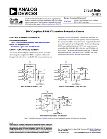
Circuit NoteCN-0313Circuits from the Lab reference circuits are engineered andtested for quick and easy system integration to help solve today’sanalog, mixed-signal, and RF design challenges. For moreinformation and/or support, visit www.analog.com/CN0313.Devices Connected/Referenced 15 kV ESD-Protected, 3.3 V,12 Mbps,EIA RS-485 TransceiverADM3485EEMC Compliant RS-485 Transceiver Protection CircuitsEVALUATION AND DESIGN SUPPORTusing the ADM3485E transceiver. Each solution was tested andcharacterized to ensure that the dynamic interaction betweenthe transceiver and the protection circuit components functionscorrectly together to protect against the electrostatic discharge(ESD), electrical fast transients (EFT), and surge immunityspecified in IEC 61000-4-2, IEC 61000-4-4, and IEC 61000-4-5,respectively. The circuits offer proven protection for RS-485interfaces using the ADM3485E to the ESD, EFT, and surgelevels often encountered in harsh environments.Circuit Evaluation BoardsCN-0313 Circuit Evaluation Board (EVAL-CN0313-SDPZ)Design and Integration FilesSchematics, Layout Files, Bill of MaterialsCIRCUIT FUNCTION AND BENEFITSThe circuits shown in Figure 1 demonstrate proven and testedelectromagnetic compatibility (EMC) compliant solutions forthree protection levels for popular RS-485 communication CDS0T23-SM712TVSCDS0T23-SM712PROTECTION SCHEME 2. TVS/TBU/TISPPROTECTION SCHEME 1. 38-15-SM-RPLFDITVSCDS0T23-SM712PROTECTION SCHEME 3. TVS/TBU/GDT11250-001DEFigure 1. Three EMC Compliant ADM3485E Protection Circuits (Simplified Schematic, All Connections Not Shown)Rev. 0Circuits from the Lab circuits from Analog Devices have been designed and built by Analog Devicesengineers. Standard engineering practices have been employed in the design and construction ofeach circuit, and their function and performance have been tested and verified in a lab environment atroom temperature. However, you are solely responsible for testing the circuit and determining itssuitability and applicability for your use and application. Accordingly, in no event shall Analog Devicesbe liable for direct, indirect, special, incidental, consequential or punitive damages due to any causewhatsoever connected to the use of any Circuits from the Lab circuits. (Continued on last page)One Technology Way, P.O. Box 9106, Norwood, MA 02062-9106, U.S.A.Tel: 781.329.4700www.analog.comFax: 781.461.3113 2013 Analog Devices, Inc. All rights reserved.
CN-0313Circuit NoteCIRCUIT DESCRIPTIONThe RS-485 bus standard is one of the most widely used physicallayer bus designs in industrial and instrumentation applications.RS-485 offers differential data transmission between multiplesystems often over very long distances. Applications for RS-485include process control networks; industrial automation; remoteterminals; building automation, such as heating, ventilation, airconditioning (HVAC) and security systems; motor control; andmotion control.In these real systems, lightning strikes, power source fluctuations,inductive switching, and electrostatic discharge can causedamage to communications ports by generating large transientvoltages. Designers must ensure that equipment does not justwork in ideal conditions, but it must also work in real-worldconditions. To ensure that these designs can work in electricallyharsh environments, EMC regulations must be met.Many EMC problems are not simple or obvious and must beconsidered at the start of the product development cycle. Propersolutions and protection circuits must be part of the total designeffort and not left to the last minute. The protection circuitsmust incorporate the input and output structure of the specifictransceiver manufacturer as part of the design.Table 1. Protection Levels Offered by Each of the ThreeProtection Circuits in Figure 1Protection Scheme1. TVS2. TVS/TBU/TISP3. TVS/TBU/GDTESD8 kV contact,15 kV air discharge8 kV contact,15 kV air discharge8 kV contact,15 kV air dischargeEFT (kV)2Surge (kV)12426Figure 2 shows a photo of the EVAL-CN0313-SDPZ board. Thereare three ADM3485E devices on the board, one for eachprotection scheme. Each protection scheme provides ESD andEFT protection as described and increasing levels of surgeprotection.A complete design support package for the EVAL-CN0313SDPZ board including schematics, layout files, and bill ofmaterials can be found at www.analog.com/CN0313DesignSupport.The IEC 61000 specifications define the set of EMC immunityrequirements. Within this set of specifications, designers mustbe concerned with the following three types of high voltagetransients for data communication lines: IEC 61000-4-2 electrostatic discharge (ESD)IEC 61000-4-4 electrical fast transients (EFT)IEC 61000-4-5 surge immunityESD and EFT have similar rise times, pulse widths, and energylevels. The surge transient has longer rise times and pulse widths; asa result, the surge transient energy can be three to four orders ofmagnitude larger than the energy in an ESD or EFT transient.Due to the similarities between ESD and EFT transients, thedesign of the circuit protection can be similar. However, due tothe high energy associated with surge transients, they must bedealt with differently.11250-002Each solution protects data ports to ESD voltages of 8 kVcontact and 15 kV air discharge, and EFT voltages of 2 kV. Thedifferent solutions provide an increased level of surgeprotection up to 6 kV. Protection levels for the circuits aresummarized in Table 1.Figure 2. EVAL-CN0313-SDPZ BoardRev. 0 Page 2 of 5
Circuit NoteCN-0313The ADM3485E is a 3.3 V, low power data transceiver suitablefor half-duplex communication on multipoint transmission lines.It has a data rate up to 12 Mbps with a common-mode range onthe bus pins (A and B) of 7 V to 12 V. Data transmits on theDI pin, and it is received on the RO pin. Both the driver andreceiver outputs can be enabled or disabled, that is, put into ahigh impedance state, by changing the logic levels on the DEand RE pins, respectively.Power and ground are connected via a screw-wire connector (VCCand GND). This connector supplies all three ADM3485E devices.Logic inputs DE and RE are set using LK1 to LK6. For eachADM3485E, LK2, LK4, and LK6 relate to DE and LK1, LK3, andLK5 relate to RE. For each link, Position A connects the logic pinto VCC, Position B connects the logic pin to GND, and Position Cconnects the logic pin to the four terminal, side screw-wireconnector. The input DI and output RO pins are connecteddirectly to the four terminal screw connector.The EVAL-CN0313-SDPZ is also compatible with the AnalogDevices, Inc., ezLINX board (EZLINX-IIIDE-EBZ) and thesystem development platform (EVAL-SDP-CB1Z). Connector J8links the UART and GPIO interfaces on the SDP or the ezLINXboard to the logic I/O of the ADM3485E devices. The I/Oconnections and jumper configurations are shown in Table 2.Table 2. ezLINX and SDP I/O Connections and /GDTI/O PinROREDEDIROREDEDIROREDEDISDP/ezLINX ConnectorUART RXGPIO 0GPIO 3UART TXUART RXGPIO 1GPIO 4UART TXUART RXGPIO 2GPIO 5UART TXSelectionLK7 (A)LK1 (C)LK2 (C)LK8 (A)LK7 (B)LK3 (C)LK4 (C)LK8 (B)LK7 (C)LK5 (C)LK6 (C)LK8 (C)The ADM3485E transmitter and receiver share the same differentialbus pins (A and B). The protection circuitry is used to protectthese bus pins.In the first protection circuit, shown in Figure 1 as TVS, it uses onecomponent, the Bourns CDSOT23-SM712. This is the transientvoltage suppressor (TVS) array shown on the EVAL-CN0313SDPZ. It consists of two bidirectional TVS diodes optimized toprotect RS-485 systems with minimal overstress while allowingthe full range of the RS-485 signal and common-mode excursions.The TVS has high impedance to ground in normal operatingconditions. When an overvoltage occurs, the TVS enters intoavalanche breakdown mode and clamps the pin voltage to a safepredetermined level. It then diverts the transient current awayfrom the ADM3485E to ground.This protection scheme offers up to 8 kV contact and15 kV airdischarge ESD, 2 kV EFT, and 1 kV surge protection.As described in the CDSOT23-SM712 data sheet, the part isdesigned specifically for RS-485 devices. The next two protectionschemes add to the CDSOT23-SM712 to provide higher levelsof circuit protection against surge.In the second scheme, shown in Figure 1 as TVS/TBU/TISP,the CDSOT23-SM712 TVS provides secondary protection, andBourns TISP4240M3BJR-S provides the primary protection. TheTISP4240M3BJR-S is a totally integrated surge protector (TISP).The TISP is a solid-state thyristor. When its predetermined voltageis exceeded, the TISP provides a low impedance path to ground,diverting a majority of the transient energy away from theADM3485E.Bourns TBU-CA065-200-WH transient blocking unit (TBU) isa nonlinear overcurrent protection device between the primaryand secondary protection devices that ensures coordinationoccurs. The TBU is an overcurrent blocking device that becomesan open circuit at a predefined current. In blocking mode, TBUhas very high impedance to block transient energy. This protectionscheme offers up to 8 kV contact and15 kV air discharge ESD,2 kV EFT, and 4 kV surge protection.The third protection scheme, shown in Figure 1 as TVS/TBU/GDT, operates in a similar fashion to Protection Scheme 2. Inthis scheme, a gas discharge tube (GDT) is used instead of theTISP. The GDT protects to higher overvoltages and overcurrentsthan the TISP described in the previous protection scheme.A GDT is a gas discharge plasma device that provides a lowimpedance path to ground to protect against over voltagetransients. The selected GDT is the Bourns 2038-15-SM-RPLF.This third protection scheme offers up to 8 kV contact and15 kV air discharge ESD, 2 kV EFT, and 6 kV surge protection.The ADM3485E has a 120 Ω termination attached to the bus pins.Rev. 0 Page 3 of 5
CN-0313Circuit NoteCIRCUIT EVALUATION AND TESTApply 3.3 V to VCC to power the EVAL-CN0313-SDPZ board.The voltage can be checked on the VCC test points near eachADM3485E. The transmit and receive paths can be tested byconnecting one of the ADM3485E circuits as shown in Figure 3.A signal or pattern generator can be connected to DI. The outputsof the driver can be monitored on the A and B test points, and theoutput of the receiver can be monitored on the RO test point.Jumper configurations are also shown in Figure 3. This testsetup can apply to any of the three circuits.For IEC 61000-4-4 EFT testing, a capacitive coupling clamp isused to couple the EFT bursts onto the cable connected to thebus lines. The coupling capacitance of the clamp depends on thecable diameter, material of the cables, and cable shielding.IEC 61000-4-5 surge testing implies the use of a coupling/decoupling network (CDN) to couple the surge transient intothe bus pins. According to the specification, this must be doneusing two 80 Ω resistors for a two port test. Figure 4 shows thetest setup for surge testing. Connect the CDN to the A and Bterminals, and the common of the surge generator to theground connection of the four terminal screw PLYOSCILLOSCOPECDNB80ΩPROTECTION120Ω COMPONENTSREA80ΩDIROREDEBFigure 4. IEC 61000-4-5 Surge CDN to ADM3485E SetupA11250-003DIABCABC11250-004DEFigure 3. Transmit and Receive Test SetupAccording to IEC 61000-4-2, ESD testing implies using twocoupling methods, contact discharge and air gap discharge.Contact discharge implies the discharge gun is placed in directconnection with the port being tested. With air discharge, thecharged electrode of the discharge gun is moved toward theport under test until a discharge occurs developing an arc acrossthe air gap. Apply discharges to the screw terminal connector ofeach bus line.All protection circuits described were characterized in the labwith the ADM3485E and verified by an external independentEMC compliance test house.For further information on the ezLINX iCoupler isolated interfacedevelopment environment, go ormation on other important EMC issues can be found athttp://www.analog.com/rs485emc.Rev. 0 Page 4 of 5
Circuit NoteCN-0313LEARN MOREData Sheets and Evaluation BoardsCN-0313 Design Support ADM3485E Data SheetezLINX iCoupler Isolated Interface DevelopmentEnvironment, ezLINX Board Quick Start GuideezLINX iCoupler Isolated Interface DevelopmentEnvironment (EZLINX-IIIDE-EBZ)Certified EMC Compliant RS-485 Interface Design ToolUG-400 User Guide, ezLINX iCoupler Isolated InterfaceDevelopment Environment, Analog Devices.System Development Platform (EVAL-SDP-CB1Z)Marais, Hein. Application Note AN-960. RS-485/RS-422 CircuitImplementation Guide. Analog Devices, Inc.Electromagnetic Compatibility (EMC) Part 4-2: Testing andMeasurement Techniques–Electrostatic Discharge ImmunityTest (IEC 61000-4-2)Electromagnetic Compatibility (EMC) Part 4-4: Testing andMeasurement Techniques–Electrical Fast Transient/BurstImmunity Test (IEC 61000-4-4)CDSOT23-SM712—Surface Mount TVS Diode Data Sheet,BournsTISP4xxxM3BJ Overvoltage Protector Series (TISP4240M3BJR-S)Data Sheet, BournsTBU-CA Series—TBU High Speed Protectors (TBU-CA065200-WH) Data Sheet, BournsElectromagnetic Compatibility (EMC) Part 4-5: Testing andMeasurement Techniques–Surge Immunity Test (IEC 61000-4-5)2038 Series Miniature Symmetrical Three Electrode SurfaceMount Gas Discharge Tube (2038-15-SM-RPLF) Data Sheet,BournsREVISION HISTORY2/13—Revision 0: Initial Version(Continued from first page) Circuits from the Lab circuits are intended only for use with Analog Devices products and are the intellectual property of Analog Devices or its licensors. While youmay use the Circuits from the Lab circuits in the design of your product, no other license is granted by implication or otherwise under any patents or other intellectual property byapplication or use of the Circuits from the Lab circuits. Information furnished by Analog Devices is believed to be accurate and reliable. However, Circuits from the Lab circuits are supplied"as is" and without warranties of any kind, express, implied, or statutory including, but not limited to, any implied warranty of merchantability, noninfringement or fitness for a particularpurpose and no responsibility is assumed by Analog Devices for their use, nor for any infringements of patents or other rights of third parties that may result from their use. Analog Devicesreserves the right to change any Circuits from the Lab circuits at any time without notice but is under no obligation to do so. 2013 Analog Devices, Inc. All rights reserved. Trademarks andregistered trademarks are the property of their respective owners.CN11250-0-2/13(0)Rev. 0 Page 5 of 5
Circuits from the Lab circuits from Analog Devices have been designed and built by Analog Devices engineers. Standard engineering practices have been employed in the design and construction of each circuit, and their function and performance have been tested and verified in a lab environment at room temperature.