Transcription
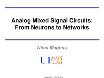
Analog Mixed Signal Circuits:From Neurons to NetworksNima MaghariAMSL ABUFUniversity of Florida
Why Analog! Signals in nature are in “Analog” formNeuron “spikes”AudioSeismicUFLAMABSUniversity of Florida2
Why Analog! Signals in nature are in “Analog” formNeuron “spikes”AudioBW 10KHzBW 24KHzSeismicBW 1HzNatural signalsoften tend to havelow/very low BWUFLAMABSUniversity of Florida2
We Invented it! We are living in a “Digital” era whereeverything and anything can be digitized!UFLAMABSUniversity of Florida3
We Invented it! We are living in a “Digital” era whereeverything and anything can be digitized!UFLAMABSUniversity of Florida3
Digital Communication Early generations– Analog modulations Modern generations– Digital modulation Everything is DigitalUFLAMABSUniversity of Florida4
Transmission Federal Communication Commission(FCC)– Assign bandwidth 1GHz 500 channels 2 MHz/channel1 2 Mbit/s010.50UFLAMABS 3 Mbit/sUniversity of Florida5
Transmission Federal Communication Commission(FCC)– Assign bandwidth 1GHz 500 channels 2 MHz/channel1 2 Mbit/s010.50UFLAMABS 3 Mbit/sUniversity of Florida5
Transmission Federal Communication Commission(FCC)– Assign bandwidth 1GHz 500 channels 2 MHz/channel1 2 Mbit/s010.50UFLAMABS 3 Mbit/sUniversity of Florida5
Transmission Federal Communication Commission(FCC)– Assign bandwidth 1GHz 500 channels 2 MHz/channel1 2 Mbit/s010.50 3 Mbit/s– Modern schemes transmit many more levelsUFLAMABSUniversity of Florida5
Transmission 8-level transmission– Ideally an 8-level ADC is sufficient to recover dataVoltsVoltsD(t)D(t)Distortion, channel nonidealities & UFLAMABSUniversity of Florida6
Transmission 8-level transmission– Ideally an 8-level ADC is sufficient to recover dataVoltsVoltsD(t)D(t)Distortion, channel nonidealities & – The signal tends to look more analog than digital!UFLAMABSUniversity of Florida6
Transmission 8-level transmission– Ideally an 8-level ADC is sufficient to recover dataUFLAMABS– The signal tends to look more analog than digital!– For both transmission and receiver we needAnalog!University of Florida6
Background Different applications. demand diff.specs– High bandwidth for data– High quality for audioUFLAMABSUniversity of Florida7
Background Different applications. demand diff.specs– High bandwidth for data– High quality for audioUFLAMABSUniversity of Florida7
Digital Links In ALL digital systems such as PC– All communication between ICs are digitalUFLAMABSUniversity of Florida8
Digital Links In ALL digital systems such as PC– All communication between ICs are digital0UFLAMABS100011University of Florida10108
Digital Links In ALL digital systems such as PC– All communication between ICs are digital0UFLAMABS100011University of Florida10108
Digital Links In ALL digital systems such as PC– All communication between ICs are digital0UFLAMABS100011University of Florida10108
Digital Links In ALL digital systems such as PC– All communication between ICs are digital0UFLAMABS100011University of Florida10108
Digital Links In ALL digital systems such as PC– All communication between ICs are digital0UFLAMABS100011University of Florida10108
Digital Links In ALL digital systems such as PC– All communication between ICs are digital01000111010MagnifiedUFLAMABSUniversity of Florida8
Digital Links In ALL digital systems such as PC– All communication between ICs are digital01000111010MagnifiedUFLAMABSUniversity of Florida8
Digital Links In ALL digital systems such as PC– All communication between ICs are digital01000111010MagnifiedUFLAMABSUniversity of Florida8
Where Else?UFLAMABSUniversity of Florida9
Where Else? Solutions:UFLAMABS– Use Adaptive filtering (FIR) Analog– Inverse Channel Filter (IIR/FIR) Analog– High-Speed ADC (3-5 bits, 10GS/s) Analog/Mixed-signalUniversity of Florida9
Background Different applications. demand diff.specs– High bandwidth for data– High quality for audioUFLAMABSUniversity of Florida10
Background Different applications. demand diff.specs– High bandwidth for data– High quality for audioUFLAMABSUniversity of Florida10
CPU/GPU and Power Management Each block has AT LEAST a singlepower management unit– As many as 10s of PM for a single blockUFLAMABSUniversity of Florida11
CPU/GPU and Power Management Each block has AT LEAST a singlepower management unit– As many as 10s of PM for a single blockUFLAMABSUniversity of Florida11
CPU/GPU and Power Management Each block has AT LEAST a singlepower management unit– As many as 10s of PM for a single block1.2V/1.5V/3.3VUFLAMABSUniversity of Florida11
CPU/GPU and Power Management Each block has AT LEAST a singlepower management unit– As many as 10s of PM for a single block1.2V/1.5V/3.3VUFLAMABSUniversity of Florida0.6V/0.9V11
CPU/GPU and Power Management Each block has AT LEAST a singlepower management unit– As many as 10s of PM for a single y of Florida0.6V/0.9V11
CPU/GPU and Power Management Each block has AT LEAST a singlepower management unit– As many as 10s of PM for a single V/5V0.5V/0.9V0.75V/1VUFLAMABSUniversity of Florida11
CPU/GPU and Power Management Each block has AT LEAST a singlepower management unit– As many as 10s of PM for a single V/5V0.5V/0.9VLi-Ion provides 3.7V!0.75V/1VUFLAMABSUniversity of Florida11
Summary Analog & Mixed-SignalAnd much more .UFLAMABSUniversity of Florida12
Analog & Mixed-Signal Solutions Most widely used analog & mixed signalcircuits are– Analog to Digital Converters (ADCs)– Digital to Analog Converters (DACs) Broad range of speed and resolution Every SoC include many–––––UFLAMABSReceiver chainClocking/PLL/DLLsPower ManagementSensing & Sensor Interface University of Florida13
Analog to Digital Conversion I Human ear can detect 16-22kHz Nyquist Sampling at 48kHz Vref-Vref How good is the quantized sinewave?UFLAMABSUniversity of Florida14
Analog to Digital Conversion I Human ear can detect 16-22kHz Nyquist Sampling at 48kHzVin VrefVrefDout-Vref How good is the quantized sinewave?UFLAMABSUniversity of Florida14
Analog to Digital Conversion II Output spectrum uency(Hz)1.524x 10SNR 10log(Psignal/Pnoise) 20dB How many levels needed for 100dB?UFLAMABSUniversity of Florida15
Analog to Digital Conversion II Output spectrum uency(Hz)1.524x 10SNR 10log(Psignal/Pnoise) 20dB How many levels needed for 100dB? 65000UFLAMABSUniversity of Florida15
Oversampling Sampling the signal faster 22.5Frequency(Hz)33.544x 10SNR 10log(Psignal/Pnoise) 23dB How much faster to get 100dB?UFLAMABSUniversity of Florida16
Oversampling Sampling the signal faster 22.5Frequency(Hz)33.544x 10SNR 10log(Psignal/Pnoise) 23dB How much faster to get 100dB? 4.4 THz!UFLAMABSUniversity of Florida16
Flash ADC Fastest among allOutput is thermometer2N comparators are needed for N bit resolution6-bit flash ADC requires 64 comparators3σoffset 7.5mV not easy! –––VinRAMSL ABUF-VrefΔUniversity of FloridaΔ Δerr(k)17
Multi-Step Concept– Take the “Residue” of the first stage andamplify/feed it to the second stageStep 1Step 2 Vref0Vj 10V20VinMeasure thedifferenceAmplify11Vj-Vref Vin(nT)GV2(nT)Dout1ADCUFLAMABSUniversity of Florida18
Multi-Step Concept– Take the “Residue” of the first stage andamplify/feed it to the second stageStep 1Step 2 Vref0Vj 10V20VinMeasure thedifferenceAmplify11 1Vj-VrefD1Vref Vin(nT)GV2(nT)Dout1CF 2D1 2CS 1VrefVCM-A 1VCM 2Vout VCMADCUFLAMABSUniversity of Florida18
Multi-Step ADC Using this approach– N bit ADC can be broken down to M P N bits– For instance, an 8-bit flash ADC (256 comp.) Can be implemented using 4 4 bits– Total of 32 comparator only! The offset/noise problem is resolved For more than two decades, this wasthe preferred approachUFLAMABSUniversity of Florida19
OpampCF AmplifierVinCS-A(s)Vout For N bit ADC, the opamp should haveminimum DC gain of 2NtotalUFLAMABSUniversity of Florida20
OpampCF AmplifierVinCS-A(s)Vout For N bit ADC, the opamp should haveminimum DC gain of 2NtotalA0 2NtotalLarge GainUFLAMABSUniversity of Florida20
OpampCF AmplifierVinCS-A(s)Vout For N bit ADC, the opamp should haveminimum DC gain of 2Ntotal For sampling frequency of fs, the BW ofopamp should be(N 1)Ntotalf3dB ln(2) fsA0 2 Large GainUFLAMABSLarge BWUniversity of Florida20
Technology Scaling Moore’s Law & CMOS process scaling– Double transistor count each 18 monthsUFLAMABSUniversity of Florida21
Technology Scaling Moore’s Law & CMOS process scaling– Double transistor count each 18 months– In terms of Analog performance & scalingVdd(V)gmrout 100543210110UFLAMABS224590180 350700 1000Lmin(nm)1022University of Florida4590180 350700 1000Lmin(nm)21
Technology Scaling Moore’s Law & CMOS process scaling– Transistors are becoming smaller & faster– Lower power, smaller area– Allows better integration In context of analog– Faster speed, but Older processVin-A(s) VoutVoutVin dBScaled processVin-Voutf A(s)UFLAMABSUniversity of Florida22
Analog Scaling Digital scales directly in terms of– Speed– Area– Power Analog–––––UFLAMABSMatchingSwitching speedDynamic rangeNoiseAreaUniversity of Florida23
Analog Scaling Digital scales directly in terms of– Speed– Area– PowerVddVddM2DinDoutM1M2DinDoutM1 Analog–––––UFLAMABSMatchingSwitching speedDynamic rangeNoiseAreaUniversity of Florida23
Analog Scaling Digital scales directly in terms of– Speed– Area– PowerVddM2DinDoutM1 VddM2DinDoutM1 Analog–––––UFLAMABSMatchingSwitching speedDynamic rangeNoiseAreaUniversity of Florida23
Analog Scaling Digital scales directly in terms ofVdd– Speed– Area– PowerMatchingSwitching speedDynamic VddM3aM2bM2aVout Vout Vb3Vb2Vout M3bM2bVout Vb1Vb1Vin Vin M 1bM 1aVin Vin M 1bM 1aVbiasUFLAMABSVddM1 Analog––––– M2VbiasMbiasMbiasUniversity of Florida23
Analog Scaling Digital scales directly in terms ofVdd– Speed– Area– PowerMatchingSwitching speedDynamic VddM3aM2bM2aVout Vout Vb3Vb2Vout M3bM2bVout Vb1Vb1Vin Vin M 1bM 1aVin Vin M 1bM 1aVbiasUFLAMABSVddM1 Analog––––– M2VbiasMbiasMbiasUniversity of Florida23
Analog ScalingInnovative Solutions are neededTo allow Analog scale well inadvanced CMOS nodesUFLAMABSUniversity of Florida24
Analog ScalingInnovative Solutions are neededTo allow Analog scale well inadvanced CMOS nodeseven with that UFLAMABSUniversity of Florida24
1GSNDR (dB) FOMWal.-Log(dB) FOMSch(dB)sf (Hz)ADCs vs. Tech. node1M180160140120140120100806040600 500UFLAMABS35025018013090Technology Node (nm)University of Florida655545 4032 2825
ADC types vs. Tech. node18Flash & 1210864700 600 50035025018013090655545 4032 28Technology Node (nm)UFLAMABSUniversity of Florida26
ADC Types– Several types ADC covering the spectrum24Resolution (ENOB)22OversampledSAR20FAST ΔΣ18161412Precision ΔΣSAR10Pipelined8 10AMSL ABUF1001K10K100K1M10M100M1GUsable Bandwidth (Hz)University of Florida27
ADC Types– Several types ADC covering the spectrum24Resolution (ENOB)22OversampledSAR20FAST ΔΣ18CT ΔΣ161412Precision ΔΣSAR10Pipelined8 10AMSL ABUF1001K10K100K1M10M100M1GUsable Bandwidth (Hz)University of Florida27
Alternative Approach: Oversampling Improving SNR for a band-limited signal– Increasing # of quantization levels smaller VLSBVLSB2q 122E– Increase the sampling frequencyPSDPSD2VLSB1 12 fsfs 2UFLAMABSfs22VLSB1 12 Nfsffs2University of FloridaNfs228
Oversampling Doubling the oversampling ratio (OSR)– Halves the quantization power– Increases SNR by 3dBfsOSR 2fB 4-bit flash ADC @ 100 MHz– OSR 1 (Nyquist) SNR 25.7dB– OSR 4SNR 31.7dBUFLAMABSUniversity of Florida29
Noise-Shaping & Oversampling Using both oversampling and noiseshapingPSDPSDBWLSB 212 f sfs2UFLAMABSfN fs2University of Floridaf30
Noise-Shaping & Oversampling Using both oversampling and noiseshapingPSDPSDBWLSB 212 f sfs2UFLAMABSf ( z)fN fs2University of Floridaf30
Noise-Shaping & Oversampling Using both oversampling and noiseshapingPSDPSDBWLSB 212 f sfs2UFLAMABSf ( z)fN fs2University of Floridaf30
Frequency Domain AnalysisY(n) qE (n) qE (n 1) By taking the Z-transform Y(z) (1 z 1)qE (z)NTF NTF 2– The NTF above is4f0.5fsThe quantization noise is shaped by the NTF filtering, and much of itis pushed to the NyquistUFLAMABSUniversity of Florida31
Implementation We are aiming to implementY(z) (1 z 1 )qE (z)– For a Nyquist quantizerqE1XQ1qE1LinearmodelYXY– For first-order noise shapingqE1XQ1 1Y(z) X(z) (1 z )qE (z)Yz 1UFLAMABSUniversity of Florida32
Output Spectrum– OSR 32, Q-levels 3SNDR 51.961dBPSD zed sampling frequencyOutput0.50-0.5AMSL ABUF1.311.3151.32SampleUniversity of Florida1.3251.331.335x 10433
Opamp Gain Ideal integratorCI 1E1 1Xz1 z 1Q1YVin 2CS 2 1AVout Limited opamp DC gain (A)H(z)limitedz 1 1 (1 1/ A)z 1 NTF would beNTF 1 (1 1/ A )z 1UFLAMABSUniversity of Florida34
Opamp Gain Ideal integratorCI 1E1 1Xz1 z 1Q1YVin 2CS 2 1AVout Limited opamp DC gain (A)H(z)limitedz 1 1 (1 1/ A)z 1 NTF would beNTF 1 (1 1/ A )z 1UFLAMABSUniversity of FloridaZero moved by 1/A34
Opamp Gain Depending on OSR– High OSR Opamp gain dominates– Low OSR Quantization noise dominates20Magnitude (dB)0Ideal opamp46dB Gain-20-40-60-80-10010-410-310-210-1100Normalized Frequency )UFLAMABSUniversity of Florida35
Opamp Gain Depending on OSR– High OSR Opamp gain dominates– Low OSR Quantization noise dominates20Magnitude (dB)0Ideal opamp46dB GainSeems as bad!-20-40-60-80-10010-410-310-210-1100Normalized Frequency )UFLAMABSUniversity of Florida35
Theoretical gain-error effectqE1–2ndOrder DSMaz 11 z 1Xbz 1 VQ1 z 1YQ1Gain-error effect in 1st and 2nd order modulators ( 0.99)2010first-ordersecond-order0Magnitude (dB)-10-20-30-40-50-60-70-8010-2-110Normalized Frequency ( rad/sample)100– Further improvement using higher order DSMUFLAMABSUniversity of Florida36
Continuous-Time ΔΣ CT integrator Vs. DT––––No sampling switch No sampling cap Better Settling and Slewing RC Variation CFCF 2 1Vref-Vref VCMUFLAMABS-A 1RVout (n)XRDAC VCMz 11 z 1 DACUniversity of FloridaAVout (t) VCMVref- 2CSVref X 1ks37
ΔΣ Modulators Trade-off (Figure of Merit)– High SQNR– High bandwidth– Low PowerPowerBWSNDR Back-end quantizer– Typically Flash– Memoryless– Large power 2E1QYbnUniversity of Florida38
Traditional Dual-Slope Simple ADC using time as media– Signal is sampled in one phase, Discharged in theother phase– Discharging time quantized by fast clock reset-VDSC 2 2 1 2RVDSX count 1tVrefTimingControl &Counter count0 12t3Dout 3Stop countDout (n) X(n) qe (n)UFLAMABSUniversity of Florida39
Noise-Shaped Integr. Quant. Small modification– Input is sampled in the same fashion– Discharging until the next edge after zero crossing-VDSC 2 2 1 2RVDSX count 1tVrefModifiedTimingControl &CounterUFLAMABS countUniversity of Florida0 12t3Dout 3Stop count40
Noise-Shaped Integr. Quant. Small modification– Input is sampled in the same fashion– Discharging until the next edge after zero crossing-VDSC 2 2 1 2RVDSX count 1tVrefModifiedTimingControl &Counter count0 12t3Dout 3Stop countDout(n) X(n) – qe(n-1) qe(n)Dout(z) X(z) (1 - z-1)·qe(z)UFLAMABSUniversity of Florida41
Noise-Shaped Integr. Quant. Small modification– Input is sampled in the same fashion– Discharging until the next edge after zero crossing-VDSC 2 2 1 2RVDSX count 1tVrefModifiedTimingControl &Counter count0 12t3Dout 3Stop countDout(n) X(n) – qe(n-1) qe(n) Scales with CMOSDout(z) X(z) (1 - z-1)·qe(z)UFLAMABSUniversity of Florida41
Double Noise-Shaped Quantizer Double Noise-Shaped Quantizer– Working in Time/Phase KTinCouterCLK1-z-1Diff.DoutTinGROoutqe(1)-qe(1) qe(2)-qe(2) qe(3)NSIQPhasesϕd2 tVDSɸDVREFɸdischa.ɸcountɸdischa.Timing control& qe gen.qe timeenqe timeGRO(1-z-1)GRO enableGROPhasesUFLAMABSD1Douttqe in timeNSIQRX-qe1(n)ϕd1CNSQ1ɸSNSQ2tXORs (1-z-1)GRO based QuantizerUniversity of FloridaD2
CT DSM Architecture DNSQ and digital integrator at back-end– Fabricated in 130nm node– 6-bit Double Noise Shaped Quantizerϕ1DLL/Clock outqe(1)-qe(1) qe(2)-qe(2) qe(3)C2R1-R2- Xkqs3 3z-16YR4GRODAC31.5 3bRZRZDAC21.5 3bNRZDAC13 sity of Florida43
Performance Comparison Measured fabricated prototype– Bested every performance down to 28nm nodeNSIQ Digital Int.DNSQfs 640 MHz BW 15 MHz- VLSI 2015- JSSC 2016- ISSCC 2017- Invited JSSC 2017 (to appear)UFLAMABSSponsored by Qualcomm Inc.University of Florida44
Future work How far we can make scale ADCsefficiently in nanometer CMOS nodes? BW limitations? Are we ready for portable 5G? Currently investigating these funded bySponsored by Semiconductor Research Corp (SRC)And Qualcomm Inc.UFLAMABSUniversity of Florida45
Where Were We ADC pioneers– 11-bit 50ks/S SAR ADCPFOM 2 BW 2ENOBAMSL ABUFJConv.Step– FoM 2.88µJ/ Conv. StepUniversity of Florida46
Where We Are Latest ADCs in same performancerange with 2fJ/Conv. StepUFLAMABSUniversity of Florida47
Where We Are Latest ADCs in same performancerange with 2fJ/Conv. Step– Improvement of 1.44 Billion times!UFLAMABSUniversity of Florida47
Where We Are Latest ADCs in same performancerange with 2fJ/Conv. Step– Improvement of 1.44 Billion times!– Not to mention the size reduction (0.1mm2)UFLAMABSUniversity of Florida47
Where We Are Latest ADCs in same performancerange with 2fJ/Conv. Step– Improvement of 1.44 Billion times!– Not to mention the size reduction (0.1mm2) If vehicles followed the sameUFLAMABSUniversity of Florida47
Where We Are Latest ADCs in same performancerange with 2fJ/Conv. Step– Improvement of 1.44 Billion times!– Not to mention the size reduction (0.1mm2) If vehicles followed the same– In 1960s, the average MPG was about 8UFLAMABSUniversity of Florida47
Where We Are Latest ADCs in same performancerange with 2fJ/Conv. Step– Improvement of 1.44 Billion times!– Not to mention the size reduction (0.1mm2) If vehicles followed the same– In 1960s, the average MPG was about 8 Improvement with factor of 1.44BillionmeansUFLAMABSUniversity of Florida47
Where We Are Latest ADCs in same performancerange with 2fJ/Conv. Step– Improvement of 1.44 Billion times!– Not to mention the size reduction (0.1mm2) If vehicles followed the same– In 1960s, the average MPG was about 8 Improvement with factor of 1.44Billionmeans– With one drop of fuel (0.1cc) you can driveround the earth 12 times!UFLAMABSUniversity of Florida47
Power Management Generate various DC voltages3.7VLi-Ion Battery1.4VDC/DC Conv.2VDC/DC Conv.LDO1.2VLDO1.8V Low-Dropout Regulators (LDO)––––Clean voltage rippleFast transient responseMin. powerNeed fast opampVinVrefLoop FilterLarge passtransistorVout Suffers from the same fate as ADCsUFLAMABSUniversity of Florida48
Fully Synthesizable Time-Based LDO– All logic based (except pass AMLOGICPAChargePump ArrayCP1 [0:31]CLKPWCLKDLL &TimingPWAMLOGICPAVDDCLPCFFChargePump ArrayCP2 [0:31]VOUTR1CVCDLIOUTNo off-chipCapacitorUFLAMABSUniversity of FloridaR249
Fully Synthesizable Time-Based LDO– All logic based (except pass AMLOGICPAChargePump ArrayCP1 [0:31]CLKPWPWAMLOGICDLL &TimingCLKPAVDDCLPCFFChargePump ArrayCP2 [0:31]VOUTR1CVCDLIOUTφRPre-ampφSNo UFLAMABSφSφDUniversity of Florida49
Fully Synthesizable Time-Based LDO– All logic based (except pass AMLOGICPACLPChargePump ArrayCP1 [0:31]CLKPWDLL &TimingCLKPWAMLOGICPAVDDCFFChargePump ArrayCP2 [0:31]VOUTR1CVCDLIOUTNANDHigh & Low Tri-stateUPNORNo off-chipCapacitorR2DNCCPUFLAMABSUniversity of Florida50
Fully Synthesizable Time-Based LDO– All logic based (except pass AMLOGICPAChargePump ArrayCP1 [0:31]CLKPWCLKPWAMLOGICDLL &TimingPAVDDCLPCFFChargePump ArrayCP2 vUFLAMABSUniversity of FloridaNo off-chipCapacitorPhysicalCircuitR251
Measurement Results Measured Results– 0.13um process– Small Area (350X250um)Steady Statepower consumption 100uA350 µm250 µmPassivedevicesDigital logic MiM CapPowerTransistorTo be presented at European Solid-State Circuits (ESSCIRC)Sponsored by Analog Devices Inc (ADI)AMSUFL ABUniversity of Florida52
IMPRESS Implantable Multimodal PeripheralREcording and Stimulation System– To enable bidirectional control of prosthetic limbDARPA LUKE armUFLAMABSUniversity of Florida53
Motivation In collaboration with imec Motivation: restore– motor functionality– sensory feedback– temperature, pressure sensation for bettercontrol,.– alleviate phantom limb painUFLAMABSUniversity of Florida54
Research Goal Communication between brain ofamputee and bionic arm/hand– Bi-directional neural c handhapticfeedbackUFLAMABSsensorsUniversity of Florida55
Proposed Solution Electrode Active probe: CMOS device integrated electrodesimplanted inside the nerve AMS UFL ABbidirectional interface recording and stimulationhigh electrode count with few external connections multiplexinghigher fiber selectivity transversal intra-fascicular implantationhigher signal local amplificationlow power consumption power-efficient circuit designminimum invasiveness chip thinninglong-term biocompatibility & stability custom chip encapsulationUniversity of Florida
PackagingIrO2 electrodes depositionLaser cutting of embeddingBack-to-back gluingprobe thickness: 2x75 µm(2x hd-TIME)UFLAMABSUniversity of Florida
ENG Acquisition Chainhd-TIMEx1x16x64 Ref. ElectrodeFlex Cable Flex ADC DriverCableDriverChannelRec. Electrode16VDDHPixelAmp.64:16x164VSSHbackend IC16LPFx11:16 61SAR ADC160kΩ12160kΩ16SwitchMatrix500kHzMux 64 active electrodes AC-coupled in-pixel amplifier: 24 dB, 1 Hz HPF corner Switch-matrix select best recording electrodes without need of repositioning theprobe 16 channels for simultaneous readout Programmable Gain: 4—44 dBUFLAMABSUniversity of Florida
ENG Acquisition ChainUFLAMABShd-TIMEbackend ICFlex Cable Flex ADC DriverCableDriver160kΩ1616SAR ADC1216:1 Muxed at 31.25kHz/ch. Output driver ADC driver withprogrammable gain 12-bit 500kS/s SAR ADC synchronization MUX/ADCthrough SPI command160kΩ16Mux18University of Florida500kHz
ENG Acquisition Chainhd-TIMEFlex Cable Flex ADC DriverCableDriver16SAR ADC160kΩ1612160kΩ500kHz16Muxbondpadshermetic stack:polyimide chipALD layersglass carrier, removed after probe fabricationPt interconnectsAu tracks (350nm)20 µmBEOLSiUFLAMABSbackend IC16:1 Muxed at 31.25kHz/ch. Output driver ADC driver withprogrammable gain 12-bit 500kS/s SAR ADC synchronization MUX/ADCthrough SPI command18University of FloridaPolyimide ALDlayers
Measurement ResultsTest PCBtest inputx64prerecordeddatax16161616ENG channelENG 16:164:16Channel64Digital Ctrl12ENG MCUSPISlaveInterfacePixel Amp.FlexRef.MCUUSBBackend ICAmplitude [µV]hd-TIME ICMCU SCLKMCU CS NMCU MOSIMCU MISOIRQ NTime [ms] Acquisition of pre-recorded spikes through whole systemUFLAMABSUniversity of Florida
Physical Unclonable Function Used in––––UFLAMABSCryptographyChip identificationObfuscation University of Florida61
Physical Unclonable Function Used in––––UFLAMABSCryptographyChip identificationObfuscation University of Florida61
Our Approach Create PUF for use in Analog/MixedSignal (AMS) applications– Leverages process variations Stochastic ADC based PUF:– Easy identification in AMS chips– Can also be utilized in fully digital chips usingstandard cells– Simple design– Minimal hardware overhead with reuse ofcomponents readily available in most AMS chipsUFLAMABSUniversity of Florida62
PUF Bit Generation Inherent random input offset voltage (Vos)of each comparator is normally distributed Employ Vos to generate a single bit (OUT)– Positive Vos OUT 1– Negative Vos OUT 0UFLAMABSUniversity of Florida63
Proposed All-Digital Comparator Compared with Custom DesignTraditional CustomDesigned Comparator(2-Tail)UFLAMABSProposed All-DigitalExtended Offset Comparator(3-Tail)University of Florida64
Measurement Results Fabricated prototype*– Fabricated in 0.13µm CMOS process– Active area 0.144mm2 Normalized Intra-HD– Across VDD (0.8V – 1.4V) 2-Tail: 0.89% 3-Latch: 0.96%– Across Temp (0 C – 80 C) 2-Tail: 0.14% 3-Latch: 0.15%Sponsored by National Science Foundation (NSF)*IEEEAMS International Symposium on Hardware Oriented Security and Trust (HOST) 2017UFL ABUniversity of Florida65
Conclusions Analog signals are everywhere– Even digital data requires analog signalprocessing techniques Different applications demand differentspecs–––––Audio Very high linearity and resolutionVideo Medium BW and medium resolutionHD Video Medium BW and high resolutionBCI Very low BW and medium resolutionCommunication Large BW and mediumresolution– UFLAMABSUniversity of Florida66
Conclusions Analog signals are everywhere– Even digital data requires analog signalprocessing techniquesEverynew application Differentapplicationsdemand differentspecs up new opportunities andopens–––––Audio Very high linearity and resolutionVideo Medium BW and medium resolutionHD Video Medium BW and high resolutionBCI Very low BW and medium resolutionCommunication Large BW and mediumresolution– brings new challenges inAnalog/Mixed-Signal DomainUFLAMABSUniversity of Florida66
My Research & Sponsors Scalable ADCs– Sponsored by SRC & Qualcomm Inc. Power Management– Texas Instruments, Analog Devices Analog Mixed-Signal Security– NSF, Honeywell Implantable Electronics– DARPA Sensor Interface– NSFUFLAMABSUniversity of Florida67
Analog & Mixed-Signal Solutions Most widely used analog & mixed signal circuits are -Analog to Digital Converters (ADCs) -Digital to Analog Converters (DACs) Broad range of speed and resolution Every SoC include many -Receiver chain -Clocking/PLL/DLLs -Power Management -Sensing & Sensor Interface - 13