Transcription
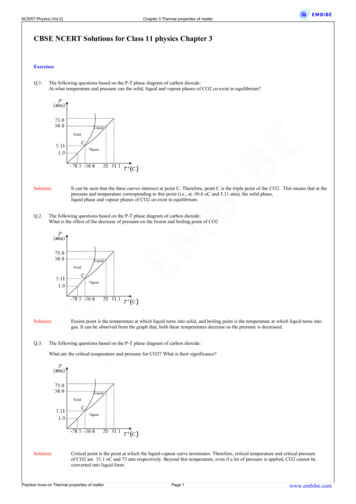
LT6203XHigh Temperature 175 CDual 100MHz, Rail-to-Rail Input and Output,Ultralow 1.9nV/ Hz Noise, Low Power Op AmpFeaturesDescriptionExtreme High Temperature Operation: –40 C to 175 Cnn Low Noise Voltage: 1.9nV/ Hz (100kHz)nn Low Supply Current: 3mA/Amp Maxnn Gain Bandwidth Product: 100MHznn Low Distortion: –80dB at 1MHznn Low Offset Voltage: 500µV Maxnn Wide Supply Range: 2.5V to 12.6Vnn Inputs and Outputs Swing Rail-to-Railnn Common Mode Rejection Ratio 90dB Typnn Low Noise Current: 1.1pA/ Hznn Output Current: 30mA Minnn 8-Pin SO Packagenn Available as DicennApplicationsDown Hole Drilling and InstrumentationHeavy Industrialnn Avionicsnn High Temperature Environmentsnn Low Noise, Low Power Signal Processingnn Active Filtersnn Rail-to-Rail Buffer Amplifiersnn Driving A/D Convertersnn DSL Receiversnn Battery Powered/Battery Backed EquipmentnnThe LT 6203X is a dual low noise, rail-to-rail input andoutput unity gain stable op amp that features 1.9nV/ Hznoise voltage and draws only 2.5mA of supply current peramplifier. These amplifiers combine very low noise andsupply current with a 100MHz gain bandwidth product, a25V/µs slew rate, and are optimized for low supply signalconditioning systems.These amplifiers maintain their performance for suppliesfrom 2.5V to 12.6V and are specified at 3V, 5V and 5Vsupplies. Harmonic distortion is less than – 80dBc at1MHz making these amplifiers suitable in low power dataacquisition systems.These devices can be used as plug-in replacements formany op amps to improve input/output range and noiseperformance.The LT6203X is a member or a growing series of high temperature qualified products offered by Linear Technology .For a complete selection of high temperature products,please consult our website, www.linear.com.nnThe LT6203X comes in an 8-pin SO package with standarddual op amp pinout. The LT6203X is also available as dice.L, LT, LTC, LTM, Linear Technology and the Linear logo are registered trademarks of AnalogDevices, Inc. All other trademarks are the property of their respective owners.Typical ApplicationLow Noise Differential Amplifier with Gain Adjust and Common Mode ControlVIN–6dB12dB0dBVIN 6dB12dBR2200ΩR3100ΩR4402ΩR10, 402ΩV –R9402Ω1/2 LT6203X V R5200ΩR6100ΩC222pFR7, 402ΩRELATIVE DIFFERENTIAL GAIN (1dB/DIV)0dBC35pFC1270pFR1402ΩLow Noise Differential AmplifierFrequency ResponseVOUT 1/2 LT6203XRA RBR8402Ω–VOUT–0.1µFOUTPUT VCM ()RBV RA RBLT6203X TA01aG 0dBG 6dBG 12dB50k1MFREQUENCY (Hz)5MLT6203X TA01b6203xfFor more information www.linear.com/LT6203X1
LT6203XAbsolute Maximum RatingsPin Configuration(Note 1)Total Supply Voltage (V to V–). 12.6VInput Current (Note 2). 40mAOutput Short-Circuit Duration(Note 3).Thermally LimitedOperating Temperature Range (Note 4)LT6203X. –40 C to 175 CJunction Temperature. 200 CStorage Temperature Range.–65 C to 200 CLead Temperature (Soldering, 10 sec). 300 CTOP VIEW 8 VOUT A 1V–– IN A 37 OUT B– –IN A 246 –IN B5 IN BS8 PACKAGE8-LEAD PLASTIC SOTJMAX 200 C, θJA 190 C/WOrder orderinfo)LEAD FREE FINISHTAPE AND REELPART MARKINGPACKAGE DESCRIPTIONSPECIFIEDTEMPERATURE RANGELT6203XS8#PBFLT6203XS8#TRPBF6203X8-Lead Plastic SO–40 C to 175 C*The temperature grade is identified by a label on the shipping containerFor more information on lead free part marking, go to: http://www.linear.com/leadfree/For more information on tape and reel specifications, go to: http://www.linear.com/tapeandreel/. Some packages are available in 500 unit reels throughdesignated sales channels with #TRMPBF suffix.Electrical Characteristicsunless otherwise noted.TA 25 C, VS 5V, 0V; VS 3V, 0V; VCM VOUT half supply,SYMBOLPARAMETERCONDITIONSVOSInput Offset VoltageVS 5V, 0V, VCM Half SupplyTYPMAX0.10.5mVVS 3V, 0V, VCM Half Supply0.61.5mVVS 5V, 0V, VCM V to V –0.252.0mV V to V �AµA4.711.3µA0.10.6µAVS 3V, 0V, VCMMINInput Offset Voltage Match(Channel-to-Channel) (Note 5)VCM Half SupplyVCM V– to V IBInput Bias CurrentVCM Half SupplyVCM V VCM V– IBIB ShiftVCM V– to V IB Match (Channel-to-Channel) (Note 5)2–7.0–8.8UNITS6203xfFor more information www.linear.com/LT6203X
LT6203XElectrical CharacteristicsTA 25 C, VS 5V, 0V; VS 3V, 0V; VCM VOUT half supply,SYMBOLPARAMETERCONDITIONSIOSInput Offset Currentunless otherwise noted.TYPMAXVCM Half SupplyVCM V VCM V–0.120.070.12111.1Input Noise Voltage0.1Hz to 10Hz800enInput Noise Voltage Densityf 100kHz, VS 5Vf 10kHz, VS 5V22.9inInput Noise Current Density, BalancedInput Noise Current Density, Unbalancedf 10kHz, VS 5V0.751.1Input ResistanceCommon ModeDifferential Mode412MΩkΩCINInput CapacitanceCommon ModeDifferential Mode1.81.5pFpFAVOLLarge Signal GainVS 5V, VO 0.5V to 4.5V, RL 1k to VS/2VS 5V, VO 1V to 4V, RL 100 to VS/2VS 3V, VO 0.5V to 2.5V, RL 1k to VS/2408.017701440V/mVV/mVV/mVCMRRCommon Mode Rejection RatioVS 5V, VCM V – to V VS 5V, VCM 1.5V to 3.5VVS 3V, VCM V– to V 6080568310080dBdBdBCMRR Match (Channel-to-Channel) (Note 5)VS 5V, VCM 1.5V to 3.5V85120dBPower Supply Rejection RatioVS 2.5V to 10V, VCM 0V6074dBPSRR Match (Channel-to-Channel) (Note 5)VS 2.5V to 10V, VCM 0V70100dBPSRRMinimum Supply Voltage (Note 6)MINUNITSµAµAµAnVP-P4.5nV/ HznV/ HzpA/ HzpA/ Hz2.5VVOLOutput Voltage Swing LOW Saturation(Note 7)No LoadISINK 5mAVS 5V, ISINK 20mAVS 3V, ISINK 15mA58524018550190460350mVmVmVmVVOHOutput Voltage Swing HIGH Saturation(Note 7)No LoadISOURCE 5mAVS 5V, ISOURCE 20mAVS 3V, ISOURCE 15mA259032522575210600410mVmVmVmVISCShort-Circuit CurrentVS 5VVS 3VISSupply Current per AmpVS 5VVS 3V2.52.3GBWGain Bandwidth ProductFrequency 1MHz, VS 5V90MHzSRSlew RateVS 5V, AV –1, RL 1k, VO 4V1724V/µs1.82.5MHz85nsFPBWFull Power Bandwidth (Note 9)VS 5V, VOUT 3VP-PtSSettling Time0.1%, VS 5V, VSTEP 2V, AV –1, RL 1k 30 25 45 40mAmA3.02.85mAmA6203xfFor more information www.linear.com/LT6203X3
LT6203XElectrical CharacteristicsThe l denotes the specifications which apply over –40 C TA 175 Ctemperature range. VS 5V, 0V; VS 3V, 0V; VCM VOUT half supply, unless otherwise noted. (Note 4)SYMBOL PARAMETERVOSVOS TCIBCONDITIONSInput Offset VoltageMINTYPMAX0.21.6UNITSVS 5V, 0V, VCM Half SupplylVS 3V, 0V, VCM Half Supplyl0.62.0mVVS 5V, 0V, VCM V to V –l1.05.0mVVS 3V, 0V, VCM V to V –l1.44.5mVInput Offset Voltage Drift (Note 8)VCM Half Supplyl3.09.0µV/ CInput Offset Voltage Match(Channel-to-Channel) (Note 5)VCM Half SupplyVCM V – to V ll0.30.71.54.0mVmVInput Bias CurrentVCM Half SupplyVCM V VCM V– 100mVlll–1.31.3–3.37.0µAµAµAl4.716.0µA V– 100mV to V –7.4–14.0mV IBIB Shiftl0.11.5µAIOSInput Offset CurrentVCM Half SupplyVCM V VCM V– 100mVlll0.20.20.21.11.61.7µAµAµAAVOLLarge Signal GainVS 5V, VO 0.5V to 4.5V, RL 1k to VS /2VS 5V, VO 1.5V to 3.5V, RL 100 toVS/2VS 3V, VO 0.5V to 2.5V, RL 1k to VS/2lll293.712601032V/mVV/mVV/mVCMRRCommon Mode Rejection RatioVS 5V, VCM V – to V VS 5V, VCM 1.5V to 3.5VVS 3V, VCM V – to V lll607550809575dBdBdBCMRR Match (Channel-to-Channel) (Note 5)VS 5V, VCM 1.5V to 3.5Vl80100dBPower Supply Rejection RatioVS 3V to 10V, VCM 0Vl6070dBPSRR Match (Channel-to-Channel) (Note 5)VS 3V to 10V, VCM 0Vl70100dBl3.0VCMIB Match (Channel-to-Channel) (Note 5)PSRRMinimum Supply Voltage (Note 6)VVOLOutput Voltage Swing LOW Saturation(Note 7)No LoadISINK 5mAISINK 15mAlll69521070220420mVmVmVVOHOutput Voltage Swing HIGH Saturation(Note 7)No LoadISOURCE 5mAVS 5V, ISOURCE 15mAVS 3V, ISOURCE rcuit CurrentVS 5VVS 3VllISSupply Current per AmpVS 5VVS 3Vll3.33.0GBWGain Bandwidth ProductFrequency 1MHzl83SRSlew RateVS 5V, AV –1, RL 1k, VO 4Vl1217V/µsFPBWFull Power Bandwidth (Note 9)VS 5V, VOUT 3VP-Pl1.31.8MHz4 15 15 25 23mAmA6.05.3mAmAMHz6203xfFor more information www.linear.com/LT6203X
LT6203XElectrical CharacteristicsSYMBOL PARAMETERVOSIBTA 25 C, VS 5V; VCM VOUT 0V, unless otherwise noted.CONDITIONSMINTYPMAXUNITSInput Offset VoltageVCM 0VVCM V VCM V –1.02.62.32.55.55.0mVmVmVInput Offset Voltage Match(Channel-to-Channel) (Note 5)VCM 0VVCM V – to V 0.20.41.02.0mVmVInput Bias CurrentVCM Half SupplyVCM V VCM V––1.31.3–3.83.0µAµAµA V– to V 5.312.5µA–7.0–9.5 IBIB Shift0.10.6µAIOSInput Offset CurrentVCM Half SupplyVCM V VCM V–0.150.20.3511.21.3µAµAµAInput Noise Voltage0.1Hz to 10Hz800enInput Noise Voltage Densityf 100kHzf 10kHz1.92.8inInput Noise Current Density, BalancedInput Noise Current Density, Unbalancedf 10kHz0.751.1Input ResistanceCommon ModeDifferential Mode412MΩkΩCINInput CapacitanceCommon ModeDifferential Mode1.81.5pFpFAVOLLarge Signal GainVO 4.5V, RL 1kVO 2.5V, RL 100751113019V/mVV/mVCMRRCommon Mode Rejection RatioVCM V – to V VCM –2V to 2V65858598dBdBCMRR Match (Channel-to-Channel) (Note 5)VCM –2V to 2V85120dBPower Supply Rejection RatioVS 1.25V to 5V6074dBPSRR Match (Channel-to-Channel) (Note 5)VS 1.25V to 5V70100dBVOLOutput Voltage Swing LOW Saturation(Note 7)No LoadISINK 5mAISINK 20mA58724550190460mVmVmVVOHOutput Voltage Swing HIGH Saturation(Note 7)No LoadISOURCE 5mAISOURCE 20mA409532095210600mVmVmVVCMIB Match (Channel-to-Channel) (Note 5)PSRRISCShort-Circuit CurrentISSupply Current per AmpGBWGain Bandwidth Product 30704.5100nV/ HznV/ HzpA/ HzpA/ Hz 402.8Frequency 1MHznVP-PmA3.5mAMHzSRSlew RateAV –1, RL 1k, VO 4V1825V/µsFPBWFull Power Bandwidth (Note 9)VOUT 3VP-P1.92.6MHztSSettling Time0.1%, VSTEP 2V, AV –1, RL 1k78nsdGDifferential Gain (Note 10)AV 2, RF RG 499Ω, RL 2k0.05%dPDifferential Phase (Note 10)AV 2, RF RG 499Ω, RL 2k0.03DEG6203xfFor more information www.linear.com/LT6203X5
LT6203XElectrical CharacteristicsThe l denotes the specifications which apply over –40 C TA 175 Ctemperature range. VS 5V; VCM VOUT 0V, unless otherwise noted. (Note 4)SYMBOL PARAMETERCONDITIONSMINTYPMAXUNITSVOSInput Offset VoltageVCM 0VVCM V VCM V –lll1.73.83.53.79.17.6mVmVmVVOS TCInput Offset Voltage Drift (Note 8)VCM Half Supplyl7.524µV/ CInput Offset Voltage Match(Channel-to-Channel) (Note 5)VCM 0VVCM V – to V ll0.30.61.23.0 0Gain Bandwidth vs Temperature100800–1000140120VS 5V, 0VVCM VS/21000PNP ACTIVEVCM 0.5V86203X G19GAIN BANDWIDTH (MHz)010PHASE MARGIN (DEG)31200UNBALANCED SOURCERESISTANCEVS 5V, 0VTA 25 CGAIN (dB)40.1Hz to 10HzOutput Voltage NoiseOUTPUT VOLTAGE (nV)612UNBALANCED NOISE CURRENT (pA/ Hz)BALANCED SOURCERESISTANCEVS 5V, 0VTA 25 CGAIN (dB)BALANCED NOISE CURRENT (pA/ Hz)7Unbalanced Noise Currentvs Frequency–20–40–6010M100MFREQUENCY (Hz)–801G6203X G256203xfFor more information www.linear.com/LT6203X9
LT6203XTypical Performance CharacteristicsGain Bandwidth and PhaseMargin vs Supply Voltage7070606012050GAIN BANDWIDTH10080RISING5040FALLING30206040AV –1RF RG 1kRL 1kVS 5VVS 2.5VVS 5VVS 2.5V1020101286TOTAL SUPPLY VOLTAGE (V)0–50 –25144Output Impedance vs Frequency10000VS 5V, 0V100OUTPUT IMPEDANCE (Ω)80SLEW RATE (V/µs)PHASE MARGIN80PHASE MARGIN (DEG)GAIN BANDWITH (MHz)TA 25 CRL 1kCL 5pFSlew Rate vs Temperature90AV 1010AV 21AV 10.10.01100k25 50 75 100 125 150 175TEMPERATURE ( C)1M10MFREQUENCY (Hz)6203X G27100M6203X G286203X G26Common Mode Rejection Ratiovs Frequency–5080TA 25 CAV 1VS 5VCOMMON MODE REJECTION RATIO (dB)100–40VS 5V, 0VVCM VS/2–60VOLTAGE GAIN (dB)COMMON MODE REJECTION RATIO (dB)120Power Supply Rejection Ratiovs FrequencyChannel Separation vs 0k1M10MFREQUENCY (Hz)100M–1200.11G110FREQUENCY (MHz)6203X G2940VS 5V, 0VAV 135OVERSHOOT (%)3025RS 20Ω15RS 50ΩRL 50Ω105NEGATIVESUPPLY201010k1k100k1MFREQUENCY (Hz)10M100MRS 10ΩRS 20Ω2520RS 50ΩRL 50Ω151050010100CAPACITIVE LOAD (pF)1000106203X G3210306203X G31VS 5V, 0VAV 230RS 10Ω20POSITIVESUPPLY40Series Output Resistorvs Capacitive LoadOVERSHOOT (%)35506203X G30Series Output Resistorvs Capacitive Load40600100VS 5V, 0VTA 25 CVCM VS/270100CAPACITIVE LOAD (pF)10006203X G336203xfFor more information www.linear.com/LT6203X
LT6203XTypical Performance CharacteristicsSettling Time vs Output Step(Noninverting)–VOUT VIN50150500Ω1mV1mV10mV10VIN500Ω–VOUT 1001mV501mV10mV–212–10OUTPUT STEP (V)34–4–3–212–10OUTPUT STEP (V)36203X G34–50–40AV 1VS 2.5VVOUT 2V(P-P)–50RL 100Ω, 3RDRL 100Ω, 2ND–60–70–80RL 1k, 3RD–90–10010kAV –1876543VS 5VTA 25 CHD2, HD3 –40dBc210k4100k1MFREQUENCY (Hz)6203X G36RL 1k, 2ND100k1MFREQUENCY (Hz)10MAV 1VS 5VVOUT 2V(P-P)RL 100Ω, 3RD–60RL 100Ω, 2ND–70–80RL 1k, 2ND–90RL 1k, 3RD–10010k100k1MFREQUENCY (Hz)6203X G37–40AV 2VS 2.5VVOUT 2V(P-P)–50Distortion vs Frequency–40–50RL 100Ω, 3RDRL 100Ω, 2ND–60–70–80RL 1k, 3RD–90–10010kAV 2RL 100Ω, 3RDVS 5VVOUT 2V(P-P)–60RL 100Ω, 2ND–70–80–90RL 1k, 3RDRL 1k, 2ND100k1MFREQUENCY (Hz)10M6203X G38Distortion vs Frequency–3010MDistortion vs FrequencyDistortion vs Frequency–4096203X G35DISTORTION (dBc)–310mV0DISTORTION (dBc)–4DISTORTION (dBc)0AV 2500Ω10mVDISTORTION (dBc)SETTLING TIME (ns)150100VS 5VAV –1TA 25 CMaximum Undistorted OutputSignal vs FrequencyOUTPUT VOLTAGE SWING (VP-P)200VS 5VAV 1TA 25 CSETTLING TIME (ns)200Settling Time vs Output Step(Inverting)10M–10010k6203X G39RL 1k, 2ND100k1MFREQUENCY (Hz)10M6203X G406203xfFor more information www.linear.com/LT6203X11
LT6203XTypical Performance Characteristics5V Large-Signal Response5V Small-Signal Response1V/DIV50mV/DIV5V0V0V200ns/DIV200ns/DIVVS 5V, 0VAV 1RL 1kVS 5V, 0VAV 1RL 1k6203X G41 5V Large-Signal Response6203X G42Output-Overdrive RecoveryVOUTVIN(2V/DIV) (1V/DIV)2V/DIV5V0V–5V0V0V200ns/DIVVS 5VAV 1RL 1k200ns/DIV6203X G43VS 5V, 0VAV 26203X G44Pin FunctionsOUT A (Pin 1): Amplifier A Output. The output swingsrail-to-rail and can source/sink a minimum of 15mA overtemperature.–IN A (Pin 2): Inverting Input of Amplifier A. Valid inputrange is from V– to V . IN B (Pin 5): Non-Inverting Input of Amplifier B. Validinput range from V– to V .–IN B (Pin 6): Inverting Input of Amplifier B. Valid inputrange from V– to V . IN A (Pin 3): Non-Inverting Input of Amplifier A. Validinput range is from V– to V .OUT B (Pin 7): Amplifier B Output. The output swingsrail-to-rail and can source/sink a minimum of 15mA overtemperature.V– (Pin 4): Negative Supply Voltage. V and V– must bechosen so that 3V (V – V–) 12.6V.V (Pin 8): Positive Supply Voltage. V and V– must bechosen so that 3V (V – V–) 12.6V.126203xfFor more information www.linear.com/LT6203X
LT6203XApplications InformationAmplifier CharacteristicsFigure 1 shows a simplified schematic of the LT6203X,which has two input differential amplifiers in parallel thatare biased on simultaneously when the common modevoltage is at least 1.5V from either rail. This topologyallows the input stage to swing from the positive supplyvoltage to the negative supply voltage. As the commonmode voltage swings beyond VCC – 1.5V, current sourceI1 saturates and current in Q1/Q4 is zero. Feedback ismaintained through the Q2/Q3 differential amplifier, butwith an input gm reduction of 1/2. A similar effect occurswith I2 when the common mode voltage swings within1.5V of the negative rail. The effect of the gm reduction isa shift in the VOS as I1 or I2 saturate.R1–VThe second stage is a folded cascode and current mirror that converts the input stage differential signals to asingle ended output. Capacitor C1 reduces the unity crossfrequency and improves the frequency stability without degrading the gain bandwidth of the amplifier. Thedifferential drive generator supplies current to the outputtransistors that swing from rail-to-rail. R2I1– VDESD1Input bias current normally flows out of the and – inputs.The magnitude of this current increases when the inputcommon mode voltage is within 1.5V of the negative rail,and only Q1/Q4 are active. The polarity of this currentreverses when the input common mode voltage is within1.5V of the positive rail and only Q2/Q3 are active.Q5Q2D1D2Q3Q1C1Q4Q9DESD4–VQ11Q7Q8 VCM V–DESD3VBIASQ6DESD2 V VDESD5DIFFERENTIALDRIVEGENERATORDESD6Q10 –VR3R4I2R5D3V–6203X F01Figure 1. Simplified Schematic6203xfFor more information www.linear.com/LT6203X13
LT6203XApplications InformationInput ProtectionThere are back-to-back diodes, D1 and D2, across the and – inputs of these amplifiers to limit the differentialinput voltage to 0.7V. The inputs of the LT6203X do nothave internal resistors in series with the input transistors.This technique is often used to protect the input devicesfrom over voltage that causes excessive currents to flow.The addition of these resistors would significantly degradethe low noise voltage of these amplifiers. For instance, a100Ω resistor in series with each input would generate1.8nV/ Hz of noise, and the total amplifier noise voltagewould rise from 1.9nV/ Hz to 2.6nV/ Hz. Once the inputdifferential voltage exceeds 0.7V, steady state currentconducted though the protection diodes should be limitedto 40mA. This implies 25Ω of protection resistance pervolt of continuous overdrive beyond 0.7V. The input diodes are rugged enough to handle transient currents dueto amplifier slew rate overdrive or momentary clippingwithout these resistors.Figure 2 shows the input and output waveforms of theamplifier driven into clipping while connected in a gainof AV 1. When the input signal goes sufficiently beyondthe power supply rails, the input transistors will saturate.When saturation occurs, the amplifier loses a stage ofphase inversion and the output tries to change states.Diodes D1 and D2 forward bias and hold the output withina diode drop of the input signal. In this photo, the inputsignal generator is clipping at 35mA, and the outputtransistors supply this generator current through theprotection diodes.With the amplifier connected in a gain of AV 2, the outputcan invert with very heavy input overdrive. To avoid thisinversion, limit the input overdrive to 0.5V beyond thepower supply rails.ESDThe LT6203X has reverse-biased ESD protection diodeson all inputs and outputs as shown in Figure 1. If thesepins are forced beyond either supply, unlimited currentwill flow through these diodes. If the current is transientand limited to one hundred milliamps or less, no damageto the device will occur.NoiseThe noise voltage of the LT6203X is equiva lent to thatof a 225Ω resistor, and for the lowest possible noiseit is desirable to keep the source and feedback resistance at or below this value, i.e. RS RG RFB 225Ω.With RS RG RFB 225Ω the total noise of the amplifieris: en (1.9nV)2 (1.9nV)2 2.7nV. Below this resis tance value, the amplifier dominates the noise, but in theresistance region between 225Ω and approximately 10kΩ,the noise is dominated by the resistor thermal noise. Asthe total resistance is further increased, beyond 10k, thenoise current multiplied by the total resistance eventuallydominates the noise.The product of en ISUPPLY is an interesting way to gaugelow noise amplifiers. Many low noise amplifiers with lowen have high ISUPPLY current. In applications that requirelow noise with the lowest possible supply current, thisproduct can prove to be enlightening. The LT6203X has anen, ISUPPLY product of 3.2 per amplifier, yet it is commonto see amplifiers with similar noise specifications have anen ISUPPLY product of 4.7 to 13.5.OVFigure 2. VS 2.5V, AV 1 with Large Overdrive14For a complete discussion of amplifier noise, see theLT1028 data sheet.6203xfFor more information www.linear.com/LT6203X
LT6203XPackage DescriptionPlease refer to http://www.linear.com/product/LT6203X#packaging for the most recent package drawings.S8 Package8-Lead Plastic Small Outline (Narrow .150 Inch)(Reference LTC DWG # 05-08-1610 Rev G).050 BSC.189 – .197(4.801 – 5.004)NOTE 3.045 .0058.245MIN.160 .0055.150 – .157(3.810 – 3.988)NOTE 31RECOMMENDED SOLDER PAD LAYOUT.010 – .020 45 (0.254 – 0.508)234.053 – .069(1.346 – 1.752).004 – .010(0.101 – 0.254)0 – 8 TYP.016 – .050(0.406 – 1.270)NOTE:1. DIMENSIONS IN6.228 – .244(5.791 – 6.197).030 .005TYP.008 – .010(0.203 – 0.254)7.014 – .019(0.355 – 0.483)TYPINCHES(MILLIMETERS)2. DRAWING NOT TO SCALE3. THESE DIMENSIONS DO NOT INCLUDE MOLD FLASH OR PROTRUSIONS.MOLD FLASH OR PROTRUSIONS SHALL NOT EXCEED .006" (0.15mm)4. PIN 1 CAN BE BEVEL EDGE OR A DIMPLE.050(1.270)BSCSO8 REV G 02126203xfInformation furnished by Linear Technology Corporation is believed to be accurate and reliable.However, no responsibility is assumed for its use. Linear Technology Corporation makes no representation that the interconnectionof its circuitsas describedherein will not infringe on existing patent rights.For moreinformationwww.linear.com/LT6203X15
LT6203XTypical ApplicationLow Noise Differential Amplifier with Gain Adjust and Common Mode Control0dBVIN–6dB12dB0dBVIN 2pFR7, 402ΩVOUT R10, 402ΩV –R9402Ω1/2 LT6203X 1/2 LT6203XRAV R5200Ω RBR6100Ω–VOUT–0.1µFR8402ΩOUTPUT VCM ()RBV RA RBLT6203X TA02aRELATIVE DIFFERENTIAL GAIN (1dB/DIV)Low Noise Differential AmplifierFrequency ResponseG 0dBG 6dBG 12dB50k1MFREQUENCY (Hz)5MLT6203X TA02bRelated PartsPART NUMBERDESCRIPTIONCOMMENTSLT1028Single, Ultralow Noise 50MHz Op Amp0.85nV/ HzLT1677Single, Low Noise Rail-to-Rail Amplifier3V Operation, 2.5mA, 4.5nV/ Hz, 60µV Max V0SLT1722/LT1723/LT1724Single/D
n Extreme High Temperature Operation : -40 C to 175 C n Low Noise Voltage: 1.9nV/ Hz (100kHz) n Low Supply Current: 3mA/Amp Max n Gain Bandwidth Product: 100MHz n Low Distortion: -80dB at 1MHz n Low Offset Voltage: 500µV Max n Wide Supply Range: 2.5V to 12.6V n Inputs and Outputs Swing Rail-to-Rail n Common Mode Rejection Ratio 90dB Typ