Transcription
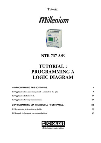
TutorialNTR 737 A/ETUTORIAL :PROGRAMMING ALOGIC DIAGRAM1/ PROGRAMMING THE SOFTWARE.31.1/ Application 1 : Access management – Automation of a gate.31.2/ Application 2 : School bell.191.3/ Application 3 : Temperature control.292/ PROGRAMMING VIA THE MODULE FRONT PANEL.332.1/ Presentation of the options available.332.2/ Example 1 : Temporary/permanent lighting.47Solutions in automation
PROGRAMMING A LOGIC DIAGRAMProgramming the softwareSCHEDULE OF REVISIONSREV. NODATEAMAY 1999ITEMFirst edition2
PROGRAMMING A LOGIC DIAGRAMProgramming the software1/ Programming the software.The software can be installed in one of the five available languages (English, German,French, Italian, Spanish).1.1/ Application 1 : Access management – Automation of a gate.This section will deal with an example of automation of a gate as shown in figure 1.1.Closing (O2)Opening (O1)Movementdetector (I4)Limit switchesClosed (I2)Open (I3)Motor with twodirections ofrotation : O1and O2Remote control signal : I1Fig. 1.1 Automation of a gate (schematic diagram)Operation :!If the gate is closed or partially open, the remote control signal causes thegate to open fully unless another remote control signal is activated.!If the gate is open, it starts to close after 4 seconds unless the movementdetector is activated.!During closing, the gate opens fully if the movement detector is activated.3
PROGRAMMING A LOGIC DIAGRAMProgramming the softwareThe logic diagram which corresponds to this type of operation (figure 1.2) can be deducedeasily and intuitively.Remote control (pulse) I1Limit switch closedI2Limit switch open I3Movement detectorI4PASNOTOPEN 1&MemorySet/ResetORTIMERDelayPriority resetANDCLOSE 1MemorySet /ResetTIMERDelayPriority resetORFig. 1.2 Logic diagram of automation of a gate.1.1.1/ Fast and easy programming.Before starting programming, the following two steps should be performed :!Make a list of the number of inputs and outputs to be used.I1I2I3I4INPUTSRemote control signalLimit switch closedLimit switch openMovement detectorO1O2OUTPUTSGate openingGate closing!Launch the application and select a module (4-2 ; 6-4 or 12-8), see figure 1.3.4
PROGRAMMING A LOGIC DIAGRAMProgramming the softwareThe example shown requires a module with 4 inputs and 2 outputs.Fig. 1.3 Selecting the number of inputs and outputs.!Select the IN key to define the type of inputs to beinserted in the diagram (figure 1.4).Fig. 1.4!Choice of inputs (figure 1.5) :Note: If necessary, use the slider indicator (scroll bar) to access thecomplete list of inputs.1-Place the mouse cursor on the required icon(pushbutton).2-Click once with the left mouse button. The mouse pointerwill display a cross on the workscreen (or FBD: FunctionBlock Diagram) if the selection is correct.Slider indicator (scroll bar) offeringaccess to all the available elements.Fig. 1.55
PROGRAMMING A LOGIC DIAGRAMProgramming the software3-Position the cross in one of the empty boxes numbered I01 to I04.Fig. 1.6 Step 44-Click once in this zone to complete the entry.Fig. 1.7 Step 55-Repeat operations 1, 2, 3 and 4 to place the three other inputs shown below :Position contactor :Position contactor :Proximity switch :The screen obtained is as follows (figure 1.8) :Fig. 1.8 Inputs in place.6
PROGRAMMING A LOGIC DIAGRAMProgramming the software!Select the OUT key to define the type of outputs to beused (figure 1.9).Fg. 1.9! Choice of outputs (figure 1.10) :The procedure is exactly the same as that for inputs. The motorwith two directions of rotation will be assimilated by two separateoutputs.The diagram is as follows (figure 1.11) :"Fig. 1.10Fig. 1.11 The inputs and outputs are positioned.!Choice of functions :via the LOGI menu (figure 1.12).* Logic functions are accessedFig. 1.12* More advanced functions(function blocks) are accessed via the FUNC menu (figure 1.13).Fig. 1.13!Positioning the blocks.Note : Selecting the blocks is similar to selecting the inputs/outputs.If a block is positioned too close to the limits of the working window (F.B.D.), an errormessage will appear.It is possible to extend the window. To do this, place the pointer on one of the edgesof the F.B.D. and, holding down the left-hand button, move the window.1-Select an AND logic block from the LOGI menu (logic functions, figure 1.14).2-Place this in the F.B.D.AND blockFig. 1.147
PROGRAMMING A LOGIC DIAGRAMProgramming the software3-Place one OR logic block, then another.4-Place a NOT logic block.5-Place one SET/RESET function block (FUNC menu fig. 1.15), then another.Fig. 1.156-Place one DELAY function block, then another.8
PROGRAMMING A LOGIC DIAGRAM!Make the connections.Programming the softwareTitFig. 1.16 Arrangement of blocks before connection.Connection rules :# Connections are made from the output of one block to the input ofanother block.# An output can be connected to several inputs.# An input can only be connected to a single output.# For successful connection, the mouse pointer must be correctlypositioned on the special marks.Discrete inputsAnalogue outputDiscrete output# An analogueue output (or input) cannot be linked to a discrete input (oroutput).# Connection is only possible if the corresponding mode is activated.Wiring connections# Removing a connection : Click on it with the left-hand button then pressDelete on the keyboard or select Clear from the drop-down Edit menu.1-Activate wiring mode (see above): the icon is highlighted.2-Place the mouse cursor on the I1 output, keeping the left-hand button pressed.3-Drag the pointer to one of the inputs on the OR block (B02) (figure 1.17).4-Release the mouse button (see figure 1.18 or 1.19).Fig. 1.17 Connection in progress.Fig. 1.18 Connection complete.9
PROGRAMMING A LOGIC DIAGRAMProgramming the softwareFig. 1.19 Error message: the connection hasnot been made. Repeat steps 2, 3, 4.5-Repeat the operation to link I2 to the input on the NOT block (B04), and to one of theinputs on the OR block (B03).6-Connect I3 to the SET input on the SET/RESET block (B06), then to the RESET inputon the SET/RESET block (B05).7-Connect I4 to one of the inputs on the AND block (B01).8-Connect the output on the NOT block (B04) to one of the inputs on the AND block (B01).10
PROGRAMMING A LOGIC DIAGRAMProgramming the software9-Connect the output on the AND block (B01) to one of the inputs on the OR block (B02).10-Connect the output on the OR block (B02) to the SET input on the SET/RESET block(B05), then to one of the inputs on the OR block (B03).11-Connect the output on the SET/RESET block (B05) to the discrete input on the DELAY block (B07).12-Connect the discrete output on the DELAY block (B07) to the output O01.13-Connect the output on the OR block (B03) to the RESET input on the SET/RESET block (B06).11
PROGRAMMING A LOGIC DIAGRAMProgramming the software14-Connect the output on the SET/RESET block (B06) to the discrete input on the DELAY block (B08).15-Connect the discrete output on the DELAY block (B08) to the output O02.16-Reposition the blocks to make the diagram clearer, figures 1.20 and 1.21 (see Generalremarks on the following page).Block in theprocess ofbeing moved.Fig. 1.20Fig. 1.21 Reorganized F.B.D.12
PROGRAMMING A LOGIC DIAGRAMGeneral remarks :Programming the software- In order to make the diagram clearer, it is possible to reorganize theelements of the F.B.D. (blocks, connection cables, inputs, outputs). To dothis, click on the element to be moved and, holding down the left mousebutton, place it in the desired position.- To move an input or an output, the mouse pointer should be positioned onthe black mark above the icon. A vertical arrow will then appear.- Comments can also be added to each block or in the F.B.D. title byMovementindicator.double-clicking on the element in question. For example, show the actionassociated with output O1 (figure 1.22) :Activating/Deactivatingthe comment.Fig. 1.22 Adding a comment.- Each of the blocks is numbered by default. This option can be inhibited bydeactivating the corresponding item.Activating/Deactivatingthe block number.Activating/Deactivatingdata on the logic state ofthe function beingsimulated.Fig. 1.23 Options for a SET/RESET function block.13
PROGRAMMING A LOGIC DIAGRAMProgramming the software!Setting the parameters for the DELAY and SET/RESET functions.1-Double-click on the DELAY function block (B07) to call up the dialogue box associatedwith the block.2-In the On Operation Delay field, enter 5 (5 x 100ms 5 tenths of a second, to stop thegate between the opening phase and the closing phase).3-In the Off operation Delay field, enter 0.4-Confirm by pressing OK.5-Double-click on the DELAY function block (B08).6-In the On operation Delay field, enter 40 (40 x 100ms 4 seconds to stop the gateopening completely).7-In the Off operation Delay field, enter 0.8-Confirm by pressing OK.14
PROGRAMMING A LOGIC DIAGRAMProgramming the software9-Double-click on the SET/RESET function block (B05).10-In the Priority field, check that the option Initialize the priority (Reset priority) ischecked.11-Confirm by pressing OK.Start/Stop Simulation icon for starting the simulation.12-Repeat steps 9, 10, 11 with the SET/RESET function block (B06).!Start simulation using the icon in the toolbar.Simulation consists of clicking on the inputs to recreate the operating conditions.15
PROGRAMMING A LOGIC DIAGRAMProgramming the software1.1.2/ DISPLAY mode.The DISPLAY block in the FUNCTION menu (figure 1.24) creates a true ManMachine Interface (M.M.I.).In certain conditions (signals given by inputs), it is possible to display processmonitoring messages on a screen.DISPLAYfunction.Fig. 1.25 Scale modificationdrop-down menuFig. 1.24!Enlarge the working window if it is too small (it is also possible to reduce the scale of theproject by changing the ZOOM – (figure 1.25).!Arrange the DISPLAY functions as shown in figure 1.26.Fig. 1.26 Adding DISPLAY functions. This block enhances the M.M.I.Theblock is an internal bit which executes forcing to 1. It enables a message to be continuouslydisplayed on the LCD screen of the module. It is accessed via the IN menu using the scroll bar (upand down arrows).16
PROGRAMMING A LOGIC DIAGRAMProgramming the software!Setting the function parameters.Double-click on block B10 then block B11. The menu shown in figure 1.27 will appear.Fig. 1.27 Window for setting the parameters of DISPLAY functions. Screens displayed simultaneously appear in thesame window. Each screen can be accessed by the corresponding tab. The text of the active block is shown in red. So,block B10 will display the current date (User option) on line Y 3 of the display. Similarly, block B11 will display thecurrent time in X 6 and Y 4. In this way the messages are not superimposed.The other two blocks, B12 (figure 1.28) and B13 (figure 1.29), show the action performed(opening or closing).Fig. 1.28 Text is displayed (String option checked in the User option menu) by entering characters (restricted to 10 perline) in the entry field in this option. The alphanumerical string can then be positioned using its X and Y coordinates.This block is connected to the output which activates opening of the gate.Fig. 1.29 This block is connected to the output which activates closing of the gate.The Opening and Closing texts can have the same coordinates since activation of the correspondingscreens is subject to two mutually exclusive conditions (i.e. the gate cannot open and close at thesame time).17
PROGRAMMING A LOGIC DIAGRAMProgramming the software!In the menu bar, select the Window drop-down menu, then the Tile option (figure 1.30).Fig. 1.30!Start the simulation using the Start/ Stop Simulation button.!A dialogue box (figure 1.31) offers to display the screen during simulation. Press Yes todisplay the interface.Fig. 1.31 Start of simulation with LCD screen display.18
PROGRAMMING A LOGIC DIAGRAMProgramming the software1.2/ Application 2 : School bell.A school wishes to install a clock which is capable of managing when bells ring during the schoolday, including holidays and bank holidays.The specifications are shown below.The bell should ring for 3 seconds, Monday to Friday at the following times :BreaksMorning0755080008500855094510 minutes 140014501455154510 minutes recreation15551600165016551745However, it should not ring during school holidays or on bank holidays :The example is based on the French holidays for 1999.School holidays (1999)Christmas: afternoon 18 December 98 to morning 4 January 99.Winter: afternoon 12 February 99 to morning 1 March 99.Easter: afternoon 09 April 99 to morning 26 April 99.Summer: afternoon 30 June 99 to morning 6 September 99.Hallowe'en : afternoon 29 October 99 to morning 8 November 99.Bank holidays (including those in the school holidays)1 January (New Year’s Day)1st Monday in April (Easter Monday)1 May (Labour Day)8 May (VE day)2nd Thursday in May (Ascension)4th Monday in May (Pentecost)14 July (Bastille Day)15 August (Assumption)11 November (Armistice Day)25 December (Christmas)Two TIME SWITCH (Clock) functions will be employed. One will manage the dailyringing of the bell, the other will switch the system off during the holidays. A ONE SHOT functionwill set the duration of the bell.19
PROGRAMMING A LOGIC DIAGRAMProgramming the softwareThe logic diagram is shown below (figure 1.32) :Clock(Time Switch)ANDDaily activation.Clock(Time Switch)ONESHOTBellDuration of bell setat 3 seconds.NOTDeactivation during holidaysFig. 1.32 Logic diagram for a school bell.The steps for selecting and positioning the blocks will be less detailed than for the previousexample. Refer back in case of difficulty.A module with 4 inputs and 2 outputs will be sufficient for this example.The output (bell) will be represented by an icon of a lamp in order to clearly identifyactivation during the simulation.1.2.1/ Positioning the blocks.!After opening a new file, taking care to select a 4/2 module, enter the title of the programto be executed by double-clicking on the Fbd title window (figure 1.33).Text toenter.UpperwindowFbd title.Dialogue boxobtained by doubleclicking on Fbdtitle.Fig. 1.3320
PROGRAMMING A LOGIC DIAGRAMProgramming the software!Select a lamp from the OUT menu to place in one of the slots reserved for outputs (figure1.34).LampFig. 1.34!Using the LOGI menu, place an AND block then a NOT block in the work screen (figure1.35). It is possible to include a comment on the output.Fig. 1.35!Using the FUNC menu, select one ONE SHOT block function and 2 TIMESW functionblocks (figure 1.36). Use the scroll bar to access one or other of these functions.Fig. 1.3621
PROGRAMMING A LOGIC DIAGRAMProgramming the software!Create the wiring (figure 1.37). To do this, activate the wiring mode.Wiring connectionsFig. 1.37Note : Arrange the blocks and connections so that the diagram is as clear as possible.1.2.2/ Positioning the blocks.The parameters for the ONE SHOT blocks (3-second pulse signal) and TIME SWITCH blocks(hourly, daily, monthly clock) must now be set.!Double-click on the ONE SHOT function block. A dialogue box (figure 1.38) promptsyou to enter the length of the signal corresponding to the time of the bell.!Enter the value 30 (30x100ms 3 s).Press the Details button in the One Shot dialogue box, and ensure that the None option has beenchecked (figure 1.39).Indication of thesignal length. Themaximum permittedvalue is 32767(which is approx.32767x100ms 54min 36 sec)Move thecursor to entera duration ofup to 10seconds(100x100ms)Fig. 1.3822
PROGRAMMING A LOGIC DIAGRAMProgramming the softwareFig. 1.39Confirm all entries by pressing OK.!Specify which should be the parameters of the 2 clock functions.The first clock deals with the time the bell is activated.Double-click on the Time Switch connected directly to the AND block (numbered B04 inthe example in this document). The dialogue box associated with it (figure 1.40) accesses severalmenus.Programmingline.Access toprogrammingoptions.Delete aprogrammingline.Transfers the dataconcerning time anddate to the module.Summer timeselectionmode.Fig. 1.4023
PROGRAMMING A LOGIC DIAGRAMProgramming the softwareNote : A single Time Switch function block can contain up to 50 programming lines (or ON/OFFcycles). A program (logic diagram) accepts 356 ON/OFF cycles, i.e. 7 clock blocks with themaximum number of cycles and 1 clock block of 6 cycles.Summer time is automatically activated according to the selection mode (see part 2of this document – “Programming via the module front panel”- to see the relevant specifications.Entering the first programming line.According to the specifications, the bell should ring at 07.55, Monday to Friday.1-From the dialogue box on figure 1.40, click on the Open/New button. The correspondingdialogue box (figure 1.41) offer three types of programming :Weekly (choice of one or more weeks per month),Daily (choice of one or more days of the week),Calendar (“date”) (choice of a specific date according to a calendar which isyear 2000 compliant (1900 to 2100)).Daily selection :If the box is not checked, it is possible to select one or more daysof the selected week(s).Weekly selection :If the box is notchecked, it ispossible to make aselection by week(A particularweek).Calendarselection :Selection of aparticular date ata specific time.Selection of thetime and theaction to beperformed (ONor OFF).Fig. 1.412-Copy the data from figure 1.41 into the dialogue box so that the clock transmits an ONsignal at 07.55 on Monday to Friday every month.3-Confirm by pressing OK.The first programming line should be as shown in figure 1.42.ON7 : 55Mon Tue Wed Thu FriEvery weekFig. 1.42In order to be able to send another ON signal to the bell, the first one must be stopped. This shouldhappen one minute later.24
PROGRAMMING A LOGIC DIAGRAMProgramming the software4-Click on the next blank programming line.5-In the Weekly Time Switch dialogue box change the time to 0756, and check the OFFbox.6-Confirm by pressing OK.The display will be as shown in figure 1.43.ONOFF7 : 557 : 56Mon Tue Wed Thu FriMon Tue Wed Thu FriEvery weekEvery weekFig. 1.43Continue in this way for all the times detailed in the specifications.Do not forget to deactivate the ON signal each time, one minute later.The grid should display the following lines (figure FONOFF7 : 557 : 568 : 008 : 018 : 508 : 518 : 558 : 569 : 459 : 469 : 559 : 5610 : 0010 : 0110 : 5010 : 5110 : 5510 : 5611 : 4511 : 4613 : 5513 : 5614 : 0014 : 0114 : 5014 : 5114 : 5514 : 5615 : 4515 : 4615 : 5515 : 5616 : 0016 : 0116 : 5016 : 5116 : 5516 : 5617 : 4517 : 46Mon Tue Wed Thu FriMon Tue Wed Thu FriMon Tue Wed Thu FriMon Tue Wed Thu FriMon Tue Wed Thu FriMon Tue Wed Thu FriMon Tue Wed Thu FriMon Tue Wed Thu FriMon Tue Wed Thu FriMon Tue Wed Thu FriMon Tue Wed Thu FriMon Tue Wed Thu FriMon Tue Wed Thu FriMon Tue Wed Thu FriMon Tue Wed Thu FriMon Tue Wed Thu FriMon Tue Wed Thu FriMon Tue Wed Thu FriMon Tue Wed Thu FriMon Tue Wed Thu FriMon Tue Wed Thu FriMon Tue Wed Thu FriMon Tue Wed Thu FriMon Tue Wed Thu FriMon Tue Wed Thu FriMon Tue Wed Thu FriMon Tue Wed Thu FriMon Tue Wed Thu FriMon Tue Wed Thu FriMon Tue Wed Thu FriMon Tue Wed Thu FriMon Tue Wed Thu FriMon Tue Wed Thu FriMon Tue Wed Thu FriMon Tue Wed Thu FriMon Tue Wed Thu FriMon Tue Wed Thu FriMon Tue Wed Thu FriMon Tue Wed Thu FriMon Tue Wed Thu FriEvery weekEvery weekEvery weekEvery weekEvery weekEvery weekEvery weekEvery weekEvery weekEvery weekEvery weekEvery weekEvery weekEvery weekEvery weekEvery weekEvery weekEvery weekEvery weekEvery weekEvery weekEvery weekEvery weekEvery weekEvery weekEvery weekEvery weekEvery weekEvery weekEvery weekEvery weekEvery weekEvery weekEvery weekEvery weekEvery weekEvery weekEvery weekEvery weekEvery weekFig. 1.4425
PROGRAMMING A LOGIC DIAGRAMProgramming the softwareProgramming the second clock which prevents the bell ringing during school and bank holidays.7-Double-click on the second clock function block in the programming screen to access thedialogue box in figure 1.45.8-Press the Open/New option.Fig. 1.459-Since holidays and bank holidays to be programmed are calendar dates, according to thespecifications, press the date option in the TimeSwitch box (figure 1.46).Fig. 1.4610-A further box will open (Define the Date Time Switch) from which it will be possible,once the Date option has been checked (step 1 figure 1.47), to enter these dates using the Calendaroption (step 2 figure 1.47).32145Fig. 1.47679826
PROGRAMMING A LOGIC DIAGRAMProgramming the software11-Once the calendar is activated, select the year of the first date (18 December 1998 in theevening, say 20.00, for example). Then, select the month of December, and then the day 18.12-Confirm by pressing OK (step 6 figure 1.47).13-Enter the hour, i.e. 20.00 (step 7 figure 1.47) and the command ON.14-Confirm by pressing OK.The command line should display the following information (figure 1.48).ON20 : 0018.12.1998DateFig : 1.48Now the clock signal needs to be deactivated for the end of the Christmas holidays on 4 January1999 in the morning at say 05.00.15-Proceed in the same way as before. The expected result is shown in figure 1.49. Becareful, this date requires the deactivation command OFF.ON20 : 00OFF5 : 00Fig : 1.4918.12.19984.1.1999DateDateThe remainder of the holidays can be programmed in the same way. However, bank holidays whichoccur each year on the same date can be recalled by the Every year option in the Define the DateTimeSwitch dialogue box (figures 1.50 and 1.51).16-For example, activate the signal on 1 January at 00.00 (figure 1.50) and deactivate it on2 January at 00.00 (figure 1.51).Fig. 1.50 Start of bank holiday.Fig. 1.51 End of bank holiday.The entry should appear as follows (figure 1.52).ON0 : 00OFF0 : 00Fig : 1.52Every Year 1 januaryEvery Year 2 januaryDateDate27
PROGRAMMING A LOGIC DIAGRAMProgramming the software17-Define all the ON/OFF cycles as shown in figure 1.53.HolidaysBank holidaysProgramming is complete.Important note : The clock whose parameters have just been set is connected to a NOT logic blockwhich can be used to reverse the output signal (see logic diagram figure 1.32). In an effort tomaximize memory space, it would have been possible to avoid inserting this block by reversing theclock signal activation and deactivation commands.28
PROGRAMMING A LOGIC DIAGRAMProgramming the software1.3/ Application 3 : Temperature control.The aim is to control the temperature of a part within a range of 20 and 18 C. Refer to previousapplications for more details regarding programming.This requires the use of a temperature/voltage converter (CROUZET Pt100 temperature probe for atemperature range of –50 to 80 C (130 degree range) with 0-10V output). The voltage is thenitself converted into a digital value on 8 bits using an A.D.C.(Analogue to Digital Converter)." 130 / 250 1 digital value every 0.5 CThe diagram shown in figure 1.54 illustrates the operation of the system :temperatureFluctuation due toinertia of thesystem.20 C18 CtimeheatingON 1timeOFF 0Fig. 1.54The part is heated to 20 C, then heating is stopped until the probe detects 18 C, then heatingrestarts.The logic diagram is as follows (figure 1.55) :Temperature converted todigital value : I01HeatingGainSCHMITTFig. 1.55 Logic diagram for temperature control.29
PROGRAMMING A LOGIC DIAGRAMProgramming the software!In the IN menu, select the analogue input (figure 1.56).Fig. 1.56!In the OUT menu, select the Heating output (figure 1.57).Fig. 1.57!From the FUNC menu, place the Gain and Trigger function blocks as shown in figure1.58.Fig. 1.58!Connect the blocks :1-Link the analogue output I01 to the analogue input of the Gain block.2-Connect the output of the Gain block to the first input of the Trigger block (figure1.58).3-Join the output of the Trigger block to the output O01.30
PROGRAMMING A LOGIC DIAGRAMProgramming the software!Set the parameters for the Gain function block.1-Double-click above to obtain the associated dialogue box (figure 1.59).Display of the gain curve :*Curve within the upperlimit 40 C, and the lowerlimit –5 C.*Slope of gain straightline 130/250.Temperaturerange from –50to 80 CNumber ofvalues from the8-bit A.D.C.Offset of theorigin bringingthe “0” of thedigital value to–50 C.Selection of scale fordrawing the curve.Fig. 1.59Values limiting thepossible range oftemperatures.2-Enter the values shown on figure 1.59 :Using the formula y (A/B)x CC : Offset -50 (offset of the origin).where x 0 : C yA : Gain numerator 130 (temperature range detectable by the probe).B : Gain denominator 250.A/B (y-C)/x (80 50)/250 130/250Upper limit 40 (limited to a detection of 40 C).Lower limit -5 (limited to a detection of –5 C).3-Press the Draw key to plot the gain curve.4-Press OK to confirm the entry.!Set the parameters of the Trigger function block. The control zone must be defined.1-Double-click above to obtain the associated dialogue box (figure 1.60).2-Enter an “ON to OFF” value of 20 C.3-Enter an “OFF to ON” value of 18 C.4-Press OK to confirm the entry.31
PROGRAMMING A LOGIC DIAGRAMProgramming the softwareGain function blockconnected to the firstanalogue input ofthe Trigger.Digital valuesdefining the controlzone.Fig. 1.60!Simulate the system by pressing the Start/Stop Simulation (see page 14) or by going tothe Controller drop-down menu and selecting the Simulation and ON option.!A digital value (temperature analogue data) is entered by clicking once on the analogueinput I01 during simulation (figure 1.61). Enter a value between 0 and 255 in the dialogue boxwhich appears.Temperature of 20 C corresponding to thedigital value entered at the input, say 135.Fig. 1.6132
PROGRAMMING A LOGIC DIAGRAMProgramming via the module front panel2/ Programming via the module front panel.The model shown here has 6 inputs and 4outputs (figure 2.1).This section explains the various menusavailable on the module, and the technique ofprogramming directly from the 8 keys on thefront panel. The examples which will illustratethe procedure are very easy.Figure 2.12.1/ Presentation of the options available.During module setup, the display is as follows (figure 2.2):TopMenuRun ProgEditProgClearTime displayInputs: The 6 circles on the linerepresent the 6 inputs. When oneof them is activated, thecorresponding circle is blackedout. In this example, input 4 (I04)is active.Outputs: The 4 outputs areshown schematically, like theinputs. Here, output 1 (O01) isactive. : Ι : οοο οο0 : οοοFig. 2.2 Screen which appearswhen the unit is first switchedon. The display is 4 lines of 10characters.Fig. 2.3 Main menuPressing one of the keys leads to the main menu (see figure 2.3).The prompt ( ) indicates which option can be selected.Note : - A flashing text is ready to be selected.- If a key which cannot be used is pressed, a question mark ( ? ) appears at the top ofthe display screen.33
PROGRAMMING A LOGIC DIAGRAMKey no.(figure 2.4)1ESC2 34OK5!6"7#8 Key no.(module)K02K03K04K01K05K06K07K08Programming via the module front panelFunctionCancels an operation, returns to previous menu.Increments, used for connecting blocks.Decrements, disconnects blocks.Accesses a menu, confirms an entry.Scrolls up.Scrolls down.Moves to the right.Moves to the left.Fig. 2.4 Key identification.Each block used occupies a memory space which mainly depends on the complexity of the function.In a program, the memory is limited to 1500 bits, and the number of blocks which can be inserted is64. The internal bits and the module keys do not occupy any bit. Connections to an output eachaccount for 10 bits.The following table summarizes all the function blocks.Memoryspace(bits)DescriptionAND (up to 4discrete inputs)19AND/ Output ON when all the inputs present are ON/ Inputs not connected areconsidered to be ON.OR (up to 4discrete inputs)19OR/ Output ON when at least one input present is ON/ Inputs not connected areconsidered to be OFF.XOR (2 discreteinputs)13EXCLUSIVE OR/ Output ON when a single input is ON.NOT (1 discreteinput)10NOT/ Reverses the signal/ Output ON if input OFF, and output OFF if inputON.NAND (up to 4discrete inputs)19NOT AND/ Output ON when at least one input present is OFF/ Inputs notconnected are considered to be OFF.19NOT OR/ Output ON when all the inputs present are OFF/ Inputs not connectedare considered to be ON.*Can be used to create logic equations between the connected inputs/ It ispossible to test the equation.Function BlockNOR (up to 4discrete inputs)BOOLEAN (up to4 discrete inputs)34
PROGRAMMING A LOGIC DIAGRAMSET/RESET14DELAY19ONE COMPARE17TIME SWITCH**GAIN22SCHMITT19ZONECOMPARE20DISPLAY***HOUR METER19Programming via the module front panelBistable memory/ Output activated by SET (discrete input), deactivated byRESET (discrete input)/ Priority assigned either to SET or RESET.Delays a signal (discrete) from a rising edge, from a falling edge, or both at thesame time/ Possible to RESET (discrete input)/ 1 digital output (value).Sends an impulse signal which can be reset/ Conditions for removing thediscrete output : deactivation of the discrete input or end of delay/ Possible toRESET (discrete input)/ 1 digital output (value).Sends a pulse from a rising edge, from a falling edge, or both at the same time/ 1discrete input/ 1 discrete output.Impulse relay function/ Alternates the output signal (discrete) on each risingedge of the input (discrete)/ Possible to RESET (discrete input)Counting incremented on each rising edge of the input (discrete)/ Possible toRESET (discrete input)/ Preset value can be assigned by a digital value/ 1discrete output/ 1 analogue output.Counting incremented (discrete input), decremented (discrete input) on eachrising edge/ Preset value can be assi
Tutorial NTR 737 A/E TUTORIAL : PROGRAMMING A LOGIC DIAGRAM 1/ PROGRAMMING THE SOFTWARE. 3 1.1/ Application 1 : Access management - Automation of a gate. 3 1.2/ Application 2 : School bell. 19 1.3/ Application 3 : Temperature control. 29 2/ PROGRAMMING VIA THE MODULE FRONT PANEL. 33 2.1/ Presentation of the options available. 33