Transcription
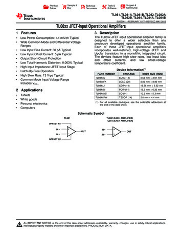
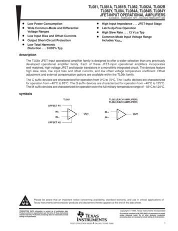
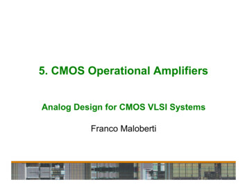
ProductFolderSample &BuySupport &CommunityTools &SoftwareTechnicalDocumentsTL081, TL081A, TL081B, TL082, TL082ATL082B, TL084, TL084A, TL084BSLOS081I – FEBRUARY 1977 – REVISED MAY 2015TL08xx JFET-Input Operational Amplifiers1 Features3 Description The TL08xx JFET-input operational amplifier family isdesigned to offer a wider selection than anypreviously developed operational amplifier family.Each of these JFET-input operational amplifiersincorporates well-matched, high-voltage JFET andbipolar transistors in a monolithic integrated circuit.The devices feature high slew rates, low input biasand offset currents, and low offset-voltagetemperature coefficient.1 Low Power Consumption: 1.4 mA/ch TypicalWide Common-Mode and Differential VoltageRangesLow Input Bias Current: 30 pA TypicalLow Input Offset Current: 5 pA TypicalOutput Short-Circuit ProtectionLow Total Harmonic Distortion: 0.003% TypicalHigh Input Impedance: JFET Input StageLatch-Up-Free OperationHigh Slew Rate: 13 V/μs TypicalCommon-Mode Input Voltage RangeIncludes VCC 2 Applications TabletsWhite goodsPersonal electronicsComputersDevice Information(1)PART NUMBERPACKAGEBODY SIZE (NOM)TL084xDSOIC (14)8.65 mm 3.91 mmTL08xxFKLCCC (20)8.89 mm 8.89 mmTL084xJCDIP (14)19.56 mm 6.92 mmTL084xNPDIP (14)19.3 mm 6.35 mmTL084xNSSO (14)10.3 mm 5.3 mmTL084xPWTSSOP (14)5.0 mm 4.4 mm(1) For all available packages, see the orderable addendum atthe end of the data sheet.Schematic SymbolTL081TL082 (EACH AMPLIFIER)TL084 (EACH AMPLIFIER)OFFSET N1IN IN OUTIN IN OUTOFFSET N21An IMPORTANT NOTICE at the end of this data sheet addresses availability, warranty, changes, use in safety-critical applications,intellectual property matters and other important disclaimers. PRODUCTION DATA.
TL081, TL081A, TL081B, TL082, TL082ATL082B, TL084, TL084A, TL084BSLOS081I – FEBRUARY 1977 – REVISED MAY 2015www.ti.comTable of Contents123456Features .Applications .Description .Revision History.Pin Configuration and Functions 5Absolute Maximum Ratings . 5ESD Ratings. 5Recommended Operating Conditions. 5Thermal Information . 6Electrical Characteristics for TL08xC, TL08xxC, andTL08xI . 6Electrical Characteristics for TL08xM and TL084x . 7Operating Characteristics. 7Dissipation Rating Table . 8Typical Characteristics . 9Parameter Measurement Information . 13Detailed Description . 148.1 Overview . 148.2 Functional Block Diagram . 148.3 Feature Description. 148.4 Device Functional Modes. 149Applications and Implementation . 159.1 Application Information. 159.2 Typical Applications . 159.3 System Examples . 1610 Power Supply Recommendations . 1811 Layout. 1811.1 Layout Guidelines . 1811.2 Layout Examples. 1912 Device and Documentation Support . 2012.112.212.312.412.512.6Documentation Support .Related Links .Community Resources.Trademarks .Electrostatic Discharge Caution .Glossary .20202020202013 Mechanical, Packaging, and OrderableInformation . 204 Revision HistoryNOTE: Page numbers for previous revisions may differ from page numbers in the current version.Changes from Revision H (January 2014) to Revision IPage Added Pin Configuration and Functions section, Storage Conditions table, ESD Ratings table, Feature Descriptionsection, Device Functional Modes, Application and Implementation section, Power Supply Recommendationssection, Layout section, Device and Documentation Support section, and Mechanical, Packaging, and OrderableInformation section . 1 Added Applications . 1 Moved Typical Characteristics into Specifications section. . 9Changes from Revision G (September 2004) to Revision HPage Updated document to new TI data sheet format - no specification changes. . 1 Deleted Ordering Information table. . 12Submit Documentation FeedbackCopyright 1977–2015, Texas Instruments IncorporatedProduct Folder Links: TL081 TL081A TL081B TL082 TL082A TL082B TL084 TL084A TL084B
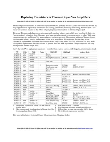
TL081, TL081A, TL081B, TL082, TL082ATL082B, TL084, TL084A, TL084Bwww.ti.comSLOS081I – FEBRUARY 1977 – REVISED MAY 20155 Pin Configuration and FunctionsTL082 FK Package20-Pin LCCCTop ViewNC1OUTNCVCC NCTL081 and TL081x D, P, and PS Package8-Pin SOIC, PDIP, and SOTop ViewNC1IN NC1IN NC43 2 1 20 1918176167158149 10 11 12 13NC2OUTNC2IN NC1OUT1IN 1IN VCC 1IN 1OUTNC4OUT4IN TL084 FK Package20-Pin LCCCTop View43 2 1 20 19185176167158149 10 11 12 138273645NCVCC OUTOFFSET N218273645VCC 2OUT2IN 2IN TL084 and TL084x D, J, N, NS and PW Package14-Pin SOIC, CDIP, PDIP, SO, and TSSOPTop View4IN NCVCC NC3IN 1OUT1IN 1IN VCC 2IN 2IN 2OUT2IN 2OUTNC3OUT3IN 1IN NCVCC NC2IN 1TL082 and TL082x D, JG, P, PS and PW Package8-Pin SOIC, CDIP, PDIP, SO, and TSSOPTop ViewNCVCC NC2IN NC5OFFSET N1IN IN VCC 11421331241151069784OUT4IN 4IN VCC 3IN 3IN 3OUTPin FunctionsPINTL081TL082TL084SOIC, PDIP,SOSOIC,CDIP, PDIP,SO, TSSOPLCCCSOIC,CDIP,PDIP, SO,TSSOP1IN–—2523INegative input1IN —3734IPositive input1OUT—1212OOutput2IN–—61569INegative input2IN —51258IPositive ve input3IN ———1014IPositive gative input4IN ———1218IPositive input4OUT———1420OOutputNAMECopyright 1977–2015, Texas Instruments IncorporatedI/OLCCCDESCRIPTIONSubmit Documentation FeedbackProduct Folder Links: TL081 TL081A TL081B TL082 TL082A TL082B TL084 TL084A TL084B3
TL081, TL081A, TL081B, TL082, TL082ATL082B, TL084, TL084A, TL084BSLOS081I – FEBRUARY 1977 – REVISED MAY 2015www.ti.comPin Functions (continued)PINTL081TL082TL084SOIC, PDIP,SOSOIC,CDIP, PDIP,SO, TSSOPLCCCSOIC,CDIP,PDIP, SO,TSSOPLCCCIN–2————INegative inputIN 3————IPositive inputNAME145688—9DESCRIPTION13NCI/O—117—Do not connect11131415161817OFFSETN11—————Input offset adjustmentOFFSETN25—————Input offset Power supplyVCC 782046—Power supply4Submit Documentation FeedbackCopyright 1977–2015, Texas Instruments IncorporatedProduct Folder Links: TL081 TL081A TL081B TL082 TL082A TL082B TL084 TL084A TL084B
TL081, TL081A, TL081B, TL082, TL082ATL082B, TL084, TL084A, TL084Bwww.ti.comSLOS081I – FEBRUARY 1977 – REVISED MAY 20156 Specifications6.1 Absolute Maximum Ratingsover operating free-air temperature range (unless otherwise noted) (1)MINVCC MAXSupply voltage (2)VCC–VIDDifferential input voltageVIInput voltage (2) (4)Operating free-air temperature0(2)(3)(4)(5)V70 CTL08 I–4085TL084Q–40125TL08 M–55125Operating virtual junction temperature(1)V 15See Dissipation Rating TableTL08 CTL08 ACTL08 BCTstg 30UnlimitedContinuous total power dissipationTCV–18(3)Duration of output short circuit (5)TAUNIT18150 CCase temperature for 60 secondsFK packageTL08 M260 CLead temperature 1,6 mm (1/16inch) from case for 10 secondsJ or JG packageTL08 M300 C150 CStorage temperature–65Stresses beyond those listed under Absolute Maximum Ratings may cause permanent damage to the device. These are stress ratingsonly, and functional operation of the device at these or any other conditions beyond those indicated under Recommended OperatingConditions is not implied. Exposure to absolute-maximum-rated conditions for extended periods may affect device reliability.All voltage values, except differential voltages, are with respect to the midpoint between VCC and VCC .Differential voltages are at IN , with respect to IN .The magnitude of the input voltage must never exceed the magnitude of the supply voltage or 15 V, whichever is less.The output may be shorted to ground or to either supply. Temperature and/or supply voltages must be limited to ensure that thedissipation rating is not exceeded.6.2 ESD RatingsVALUEV(ESD)(1)(2)Electrostatic dischargeHuman body model (HBM), per ANSI/ESDA/JEDEC JS-001 (1)1000Charged-device model (CDM), per JEDEC specification JESD22C101 (2)1500UNITVJEDEC document JEP155 states that 500-V HBM allows safe manufacturing with a standard ESD control process.JEDEC document JEP157 states that 250-V CDM allows safe manufacturing with a standard ESD control process.6.3 Recommended Operating Conditionsover operating free-air temperature range (unless otherwise noted)MINMAXUNITVCC Supply voltage515VVCC–Supply voltage–5–15VVCMCommon-mode voltageVCC– 4VCC – bient temperatureTL08xCCopyright 1977–2015, Texas Instruments IncorporatedSubmit Documentation FeedbackProduct Folder Links: TL081 TL081A TL081B TL082 TL082A TL082B TL084 TL084A TL084B C5
TL081, TL081A, TL081B, TL082, TL082ATL082B, TL084, TL084A, TL084BSLOS081I – FEBRUARY 1977 – REVISED MAY 2015www.ti.com6.4 Thermal InformationTL08xxTHERMAL METRIC (1)RθJA(1)(2)(3)Junction-to-ambientthermal resistance (2) (3)D (SOIC)N (PDIP)NS (SO)P (PDIP)PS (SO)8 PINS14PINS14 PINS14 PINS{PINCOUNT}PINS{PINCOUNT}PINS8 PINSPW (TSSOP)14PINS978676808595149113UNIT C/WFor more information about traditional and new thermal metrics, see the Semiconductor and IC Package Thermal Metrics applicationreport, SPRA953.Maximum power dissipation is a function of TJ(max), RθJA, and TA. The maximum allowable power dissipation at any allowable ambienttemperature is PD (TJ(max) – TA) / RθJA. Operating at the absolute maximum TJ of 150 C can affect reliability.The package thermal impedance is calculated in accordance with JESD 51-7.6.5 Electrical Characteristics for TL08xC, TL08xxC, and TL08xIVCC 15 V (unless otherwise noted)PARAMETERTESTCONDITIONSVIOInput offsetvoltageVO 0,RS 50 ΩαVIOTemperaturecoefficient ofVO 0,inputRS 50 ΩoffsetvoltageIIOInput offsetcurrent (2)VO 0IIBInput biascurrent (2)VO 0VICRCommonmodeinput voltagerangeVOMMaximumpeakoutputvoltageswingTA (1)TL081C, TL082C,TL084CMIN25 CRL 10 kΩRL 2 kΩTYPMAX315FullrangeMINTYPMAX3620Fullrange1825 C5Fullrange30FullrangeTL081BC, 00530720030725 C 11–12to15 11–12to15 11–12to15 11–12to1525 C 12 13.5 12 13.5 12 13.5 12 13.5Fullrange 12 12 12 12mVμV/ C182200UNITTYP9182400TL081I, TL082I,TL084I518225 CRL 10 kΩTL081AC, TL082AC,TL084AC100pA10nA200pA20nAVV 10 12 10 12 10 12 10 1225 25 C3333riInputresistance25 C VICRmin,VO 0,RS 50 Ω25 (ΔVCC /ΔVIO)VCC 15 V to 9 V,VO 0,RS 50 Ω25 C7086808680868086dB(1)(2)6VO 10 V,RL 2 kΩ1525V/mV25MHzAll characteristics are measured under open-loop conditions with zero common-mode voltage, unless otherwise specified. Full range forTA is 0 C to 70 C for TL08 C, TL08 AC, TL08 BC and –40 C to 85 C for TL08 I.Input bias currents of an FET-input operational amplifier are normal junction reverse currents, which are temperature sensitive, asshown in Figure 13. Pulse techniques must be used that maintain the junction temperature as close to the ambient temperature aspossible.Submit Documentation FeedbackCopyright 1977–2015, Texas Instruments IncorporatedProduct Folder Links: TL081 TL081A TL081B TL082 TL082A TL082B TL084 TL084A TL084B
TL081, TL081A, TL081B, TL082, TL082ATL082B, TL084, TL084A, TL084Bwww.ti.comSLOS081I – FEBRUARY 1977 – REVISED MAY 2015Electrical Characteristics for TL08xC, TL08xxC, and TL08xI (continued)VCC 15 V (unless otherwise noted)TESTCONDITIONSPARAMETERTA (1)TL081C, TL082C,TL084CMINTL081AC, fier)VO 0,No load25 C1.4VO1/VO2CrosstalkattenuationAVD 10025 C120MINTL081BC, TL082BC,TL084BCTYPMAX1.42.8MIN120TL081I, 20dB6.6 Electrical Characteristics for TL08xM and TL084xVCC 15 V (unless otherwise noted)TEST CONDITIONS (1)PARAMETERVIOInput offset voltageVO 0, RS 50 ΩαVIOTemperaturecoefficient of inputoffset voltageVO 0, RS 50 ΩIIOInput offset current (2)VO 0Input bias current (2)IIBVICRCommon-modeinput voltage rangeVOMMaximum peakoutput voltage swingTATL081M, TL082MMINTYP25 C3Full rangeFull range1825 C530125 CRL 10 kΩRL 2 kΩ25 C 1125 C 12 13.5UNITMAX639mV15μV/ C181005100pA2020030nA200pA50nA50–12to15Full rangeTYP2025 CRL 10 kΩMIN9125 CVO 0TL084Q, TL084MMAX 12 11–12to15 12 13.5V 12V 10 12 10 1225 C2520025200Full range15AVDLarge-signal differentialvoltage amplificationB1Unity-gain bandwidth25 C33MHzriInput resistance25 C1212ΩCMRRCommon-moderejection ratioVIC VICRmin,VO 0, RS 50 Ω25 C80868086dBkSVRSupply-voltagerejection ratio(ΔVCC /ΔVIO)VCC 15 V to 9 V,VO 0, RS 50 Ω25 C80868086dBICCSupply current(each amplifier)VO 0, No load25 C1.4VO1/VO2Crosstalk attenuationAVD 10025 C120(1)(2)VO 10 V, RL 2 kΩV/mV1510102.81.42.8mA120dBAll characteristics are measured under open-loop conditions, with zero common-mode input voltage, unless otherwise specified.Input bias currents of a FET-input operational amplifier are normal junction reverse currents, which are temperature sensitive, as shownin Figure 13. Pulse techniques must be used that maintain the junction temperatures as close to the ambient temperature as possible.6.7 Operating CharacteristicsVCC 15 V, TA 25 C (unless otherwise noted)PARAMETERSR(1)Slew rate at unity gainMINTYPVI 10 V, RL 2 kΩ, CL 100 pF,See Figure 19TEST CONDITIONS8 (1)13VI 10 V, RL 2 kΩ, CL 100 pF,TA 55 C to 125 C,See Figure 195 (1)MAXUNITV/μsOn products compliant to MIL-PRF-38535, this parameter is not production tested.Copyright 1977–2015, Texas Instruments IncorporatedSubmit Documentation FeedbackProduct Folder Links: TL081 TL081A TL081B TL082 TL082A TL082B TL084 TL084A TL084B7
TL081, TL081A, TL081B, TL082, TL082ATL082B, TL084, TL084A, TL084BSLOS081I – FEBRUARY 1977 – REVISED MAY 2015www.ti.comOperating Characteristics (continued)VCC 15 V, TA 25 C (unless otherwise noted)PARAMETERtrRise-timeTEST CONDITIONSMINTYP0.05overshoot factorVI 20 V, RL 2 kΩ, CL 100 pF,See Figure 19VnEquivalent input noisevoltageRS 20 ΩInEquivalent input noisecurrentRS 20 Ω,THDTotal harmonic distortionVIrms 6 V, AVD 1, RS 1 kΩ, RL 2 kΩ,f 1 kHz,MAXUNITμs20%f 1 kHzf 10 Hz to 10 kHzf 1 kHz18nV/ Hz4μV0.01pA/ Hz0.003%6.8 Dissipation Rating Table8PACKAGETA 25 CPOWER RATINGD (14 pin)FKDERATINGFACTORDERATEABOVE TATA 70 CPOWER RATINGTA 85 CPOWER RATINGTA 125 CPOWER RATING680 mW7.6 mW/ C60 C604 m/W490 mW186 mW680 mW11.0 mW/ C88 C680 m/W680 mW273 mWJ680 mW11.0 mW/ C88 C680 m/W680 mW273 mWJG680 mW8.4 mW/ C69 C672 m/W546 mW210 mWSubmit Documentation FeedbackCopyright 1977–2015, Texas Instruments IncorporatedProduct Folder Links: TL081 TL081A TL081B TL082 TL082A TL082B TL084 TL084A TL084B
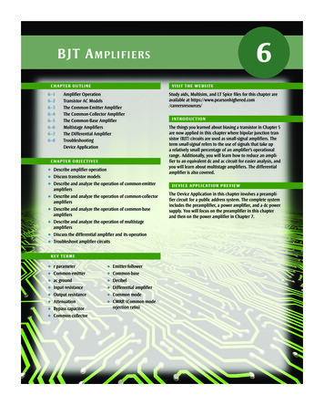
TL081, TL081A, TL081B, TL082, TL082ATL082B, TL084, TL084A, TL084Bwww.ti.comSLOS081I – FEBRUARY 1977 – REVISED MAY 20156.9 Typical CharacteristicsData at high and low temperatures are applicable only within the rated operating free-air temperature ranges of the variousdevices. The Figure numbers referenced in the following graphs are located in Parameter Measurement Information.Table 1. Table of GraphsFigureMaximum peak output voltageversusversusversusversusLarge-signal differential voltageamplificationversus Free-air temperatureversus Load resistanceFigure 7Figure 8Differential voltage amplificationversus Frequency with feed-forwardcompensationFigure 9PDTotal power dissipationversus Free-air temperatureFigure 10ICCSupply currentversus Free-air temperatureversus Supply voltageFigure 11Figure 12IIBInput bias currentversus Free-air temperatureFigure 13Large-signal pulse responseversus TimeFigure 14VOOutput voltageversus Elapsed timeFigure 15CMRRCommon-mode rejection ratioversus Free-air temperatureFigure 16VnEquivalent input noise voltageversus FrequencyFigure 17THDTotal harmonic distortionversus FrequencyFigure 18VOMAVDFrequencyFree-air temperatureLoad resistanceSupply voltage 15VCC 15 V 12.5 10RL 10 kΩTA 25 CSee Figure 2VCC 10 V 7.5VCC 5 V 5 2.501001k10 k100 kf Frequency Hz1M10 MFigure 1. Maximum Peak Output VoltagevsFrequencyCopyright 1977–2015, Texas Instruments IncorporatedVOMVOM Maximum Peak Output Voltage V 15VOMVOM Maximum Peak Output Voltage VFigure 1, Figure 2, Figure 3Figure 4Figure 5Figure 6VCC 15 V 12.5RL 2 kΩTA 25 CSee Figure 2 10VCC 10 V 7.5 5VCC 5 V 2.501001k10 k100 kf Frequency Hz1M10 MFigure 2. Maximum Peak Output VoltagevsFrequencySubmit Documentation FeedbackProduct Folder Links: TL081 TL081A TL081B TL082 TL082A TL082B TL084 TL084A TL084B9
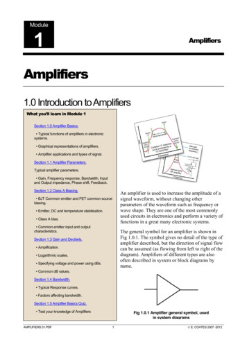
TL081, TL081A, TL081B, TL082, TL082ATL082B, TL084, TL084A, TL084BSLOS081I – FEBRUARY 1977 – REVISED MAY 2015www.ti.com 15VCC 15 VRL 2 kΩSee Figure 2TA 25 C 12.5VVOMOM Maximum Peak Output Voltage V 10TA 55 C 7.5TA 125 C 5 2.5 12.5RL 2 kΩ 10 7.5 5 2.5VCC 15 VSee Figure 2010 k40 k 100 k400 k 1 Mf Frequency Hz4M0 7510 MVOMVOM Maximum Peak Output Voltage V 7.5 5 2.580.40.7 124125 7.5 5 2.580246810121416 VCC Supply Voltage VFigure 6. Maximum Peak Output VoltagevsSupply Voltage106AAVD – Large-Signal DifferentialVoltage AmplificationAAVD Large-Signal DifferentialVoltage Amplification V/mV100 107 10400200100402010VCC 15 VVO 10 VRL 2 kΩVCC 5 V to 15 VRL 2 kΩTA 25 C105104DifferentialVoltageAmplification103102 250255075100125TA Free-Air Temperature CSubmit Documentation Feedback0 45 90 Phase Shift101135 1 50Figure 7. Large-Signal Differential Voltage AmplificationvsFree-Air Temperature107500.210001 7550 12.5Figure 5. Maximum Peak Output VoltagevsLoad Resistance225RL 10 kΩTA 25 CRL Load Resistance kΩ40 15VCC 15 VTA 25 CSee Figure 2 1000.1 25Figure 4. Maximum Peak Output VoltagevsFree-Air Temperature 15 12.5 50TA Free-Air Temperature CFigure 3. Maximum Peak Output VoltagevsFrequencyVOM Maximum Peak Output Voltage VVOMRL 10 kΩPhase ShiftVOMVOM Maximum Peak Output Voltage V 151101001k10 k 100 kf Frequency Hz1M180 10 MFigure 8. Large-Signal Differential Voltage Amplification andPhase ShiftvsFrequencyCopyright 1977–2015, Texas Instruments IncorporatedProduct Folder Links: TL081 TL081A TL081B TL082 TL082A TL082B TL084 TL084A TL084B
TL081, TL081A, TL081B, TL082, TL082ATL082B, TL084, TL084A, TL084Bwww.ti.comSLOS081I – FEBRUARY 1977 – REVISED MAY 2015250VCC 15 VC2 3 pFTA 25 CSee Figure 3105VCC 15 VNo SignalNo Load225PD Total Power Dissipation mWAVD Differential Voltage Amplification V/mV10610410310210200175TL084, TL085150125100TL082, TL08375TL081502511001k10 k100 k1M0 7510 M 5025507510012522VCC 15 VNo SignalNo Load1.81.6ICC Supply Current Per Amplifier mAI CC ICC Supply Current Per Amplifier mAI CC 0Figure 10. Total Power DissipationvsFree-Air TemperatureFigure 9. Differential Voltage AmplificationvsFrequency with Feed-Forward Compensation1.41.210.80.60.40.20 75TA 25 CNo SignalNo Load1.81.61.41.210.80.60.40.20 50 2502550751000125246810121416TA Free-Air Temperature C VCC Supply Voltage VFigure 11. Supply Current per AmplifiervsFree-Air TemperatureFigure 12. Supply Current per AmplifiervsSupply Voltage1006VI and VO Input and Output Voltages VV CC 15 VI IB Input Bias Current nA 25TA Free-Air Temperature Cf Frequency With Feed-Forward Compensation Hz1010.10.01 504Output20 2Input 4 6 250255075100TA Free-Air Temperature CFigure 13. Input Bias CurrentvsFree-Air TemperatureCopyright 1977–2015, Texas Instruments Incorporated125VCC 15 VRL 2 kΩCL 100 pFTA 25 C00.511.5t Time µs22.533.5Figure 14. Voltage-Follower Large-Signal Pulse ResponseSubmit Documentation FeedbackProduct Folder Links: TL081 TL081A TL081B TL082 TL082A TL082B TL084 TL084A TL084B11
TL081, TL081A, TL081B, TL082, TL082ATL082B, TL084, TL084A, TL084BSLOS081I – FEBRUARY 1977 – REVISED MAY 2015www.ti.com28CMRR Common-Mode Rejection Ratio dB89VO Output Voltage mV242016VCC 15 VRL 2 kΩCL 100 pFTA 25 CSee Figure 112840 40.20.40.60.81.08584 50 250255075100125Figure 15. Output VoltagevsElapsed TimeFigure 16. Common-Mode Rejection RatiovsFree-Air Temperature4030201040 100400 1 k4 k 10 kf Frequency Hz40 k 100 kFigure 17. Equivalent Input Noise VoltagevsFrequency128683 751.2VCC 15 VAVD 10RS 20 ΩTA 25 C1087TA Free-Air Temperature C 50088t Elapsed Time – µsSubmit Documentation Feedback1THD Total Harmonic Distortion %V n Equivalent Input Noise Voltage nV/HznV/ Hz0VCC 15 VRL 10 kΩVCC 15 VAVD 1VI(RMS) 6 V0.4TA 25 C0.10.040.010.0040.0011004001k4 k 10 kf Frequency Hz40 k 100 kFigure 18. Total Harmonic DistortionvsFrequencyCopyright 1977–2015, Texas Instruments IncorporatedProduct Folder Links: TL081 TL081A TL081B TL082 TL082A TL082B TL084 TL084A TL084B
TL081, TL081A, TL081B, TL082, TL082ATL082B, TL084, TL084A, TL084Bwww.ti.comSLOS081I – FEBRUARY 1977 – REVISED MAY 20157 Parameter Measurement Information10 kΩ1 kΩ VIOUTOUT VIRLCL 100 pFFigure 19. Test Figure 1Figure 20. Test Figure 2100 kΩTL081 IN C2OUTC1 500 pFN2 IN IN CL 100 pFRL 2 kΩN1100 kΩN1OUT1.5 kΩ VCC Figure 21. Test Figure 3Copyright 1977–2015, Texas Instruments IncorporatedFigure 22. Test Figure 4Submit Documentation FeedbackProduct Folder Links: TL081 TL081A TL081B TL082 TL082A TL082B TL084 TL084A TL084B13
TL081, TL081A, TL081B, TL082, TL082ATL082B, TL084, TL084A, TL084BSLOS081I – FEBRUARY 1977 – REVISED MAY 2015www.ti.com8 Detailed Description8.1 OverviewThe TL08xx JFET-input operational amplifier family is designed to offer a wider selection than any previouslydeveloped operational amplifier family. Each of these JFET-input operational amplifiers incorporates wellmatched, high-voltage JFET and bipolar transistors in a monolithic integrated circuit. The devices feature highslew rates, low input bias and offset currents, and low offset-voltage temperature coefficient. Offset adjustmentand external compensation options are available within the TL08xx family.The C-suffix devices are characterized for operation from 0 C to 70 C. The I-suffix devices are characterized foroperation from 40 C to 85 C. The Q-suffix devices are characterized for operation from –40 C to 125 C. TheM-suffix devices are characterized for operation over the full military temperature range of 55 C to 125 C.8.2 Functional Block DiagramVCC IN 64ΩIN OUT128Ω64ΩC11080Ω1080ΩVCC OFFSET N1OFFSET N2TL081 Only8.3 Feature Description8.3.1 Total Harmonic DistortionHarmonic distortions to an audio signal are created by electronic components in a circuit. Total harmonicdistortion (THD) is a measure of harmonic distortions accumulated by a signal in an audio system. These deviceshave a very low THD of 0.003% meaning that the TL08x devices will add little harmonic distortion when used inaudio signal applications.8.3.2 Slew RateThe slew rate is the rate at which an operational amplifier can change its output when there is a change on theinput. These devices have a 13-V/μs slew rate.8.4 Device Functional ModesThese devices are powered on when the supply is connected. This device can be operated as a single-supplyoperational amplifier or dual-supply amplifier depending on the application.14Submit Documentation FeedbackCopyright 1977–2015, Texas Instruments IncorporatedProduct Folder Links: TL081 TL081A TL081B TL082 TL082A TL082B TL084 TL084A TL084B
TL081, TL081A, TL081B, TL082, TL082ATL082B, TL084, TL084A, TL084Bwww.ti.comSLOS081I – FEBRUARY 1977 – REVISED MAY 20159 Applications and ImplementationNOTEInformation in the following applications sections is not part of the TI componentspecification, and TI does not warrant its accuracy or completeness. TI’s customers areresponsible for determining suitability of components for their purposes. Customers shouldvalidate and test their design implementation to confirm system functionality.9.1 Application InformationThe TL08x series of operational amplifiers can be used in countless applications. The few applications in thissection show principles used in all applications of these parts.9.2 Typical Applications9.2.1 Inverting Amplifier ApplicationA typical application for an operational amplifier in an inverting amplifier. This amplifier takes a positive voltageon the input, and makes it a negative voltage of the same magnitude. In the same manner, it also makesnegative voltages positive.RFRIVsup VOUTVIN Vsup-Figure 23. Schematic for Inverting Amplifier Application9.2.1.1 Design RequirementsThe supply voltage must be chosen such that it is larger than the input voltage range and output range. Forinstance, this application will scale a signal of 0.5 V to 1.8 V. Setting the supply at 12 V is sufficient toaccommodate this application.9.2.1.2 Detailed Design ProcedureDetermine the gain required by the inverting amplifier:(1)(2)Once the desired gain is determined, choose a value for RI or RF. Choosing a value in the kΩ range is desirablebecause the amplifier circuit will use currents in the milliamp range. This ensures the part will not draw too muchcurrent. This example will choose 10 kΩ for RI which means 36 kΩ will be used for RF. This was determined byEquation 3.(3)Copyright 1977–2015, Texas Instruments IncorporatedSubmit Documentation FeedbackProduct Folder Links: TL081 TL081A TL081B TL082 TL082A TL082B TL084 TL084A TL084B15
TL081, TL081A, TL081B, TL082, TL082ATL082B, TL084, TL084A, TL084BSLOS081I – FEBRUARY 1977 – REVISED MAY 2015www.ti.comTypical Applications (continued)9.2.1.3 Application Curve2VIN1.5VOUT1Volts0.50-0.5-1-1.5-200.51Time (ms)1.52Figure 24. Input and output voltages of the inverting amplifier9.3 System Examples9.3.1 General ApplicationsRF 100 kΩVCC OutputR1Input C3TL081 CF 3.3 µFTL081R2 15 V3.3 kΩOutputVCC 1 kΩ 15 VR1 R2 2(R3) 1.5 MΩR3C1C2C1 C2 C3 110 pF21fo 1 kHz2π R1 C13.3 kΩ9.1 kΩFigure 25. 0.5-Hz Square-Wave OscillatorFigure 26. High-Q Notch Filter 15 V18 pF TL084VCC 18 pFOutput A TL084 VCC 88.4 kΩ 100 kΩVCC 6 cos ωt1 kΩ15 V1N414888.4 kΩVCC 18 kΩ(see Note A)A. These resistor values may be adjusted for a symmetrical output.VCC 100 kΩVCC 100 µFVCC Output B 100 kΩ18 kΩ(see Note A)1/2TL08218 pFTL084100 kΩ88.4 kΩ1/2TL082 Input1 kΩVCC 1 µF1N41486 sin ωtVCC 1 MΩ 12π RF CF f TL084Output C Figure 27. Audio-Distribution Amplifier16Submit Documentation FeedbackFigure 28. 100-kHz Quadrature OscillatorCopyright 1977–2015, Texas Instruments IncorporatedProduct Folder Links: TL081 TL081A TL081B TL082 TL082A TL082B TL084 TL084A TL084B
TL081, TL081A, TL081B, TL082, TL082ATL082B, TL084, TL084A, TL084Bwww.ti.comSLOS081I – FEBRUARY 1977 – REVISED MAY 2015System Examples (continued)16 kΩ16 kΩ220 pF220 pFVCC 43 kΩ43 kΩ1/4TL084VCC VCC 43 kΩ1/4TL0841/4TL084 1.5 kΩ 1/4TL084220 pFVCC Input220 pF30 kΩ 43 kΩ43 kΩ30 kΩ1.5 kΩVCC 43 kΩVCC VCC OutputBVCC Output AOutput AOutput B2 kHz/divSecond-Order Bandpass Filterfo 100 kHz, Q 30, GAIN 42 kHz/divCascaded Bandpass Filterfo 100 kHz, Q 69, GAIN 16Figure 29. Positive-Feedback Bandpass FilterCopyright 1977–2015, Texas Instruments IncorporatedSubmit Documentation FeedbackProduct Folder Links: TL081 TL081A TL081B TL082 TL082A TL082B TL084 TL084A TL084B17
TL081, TL081A, TL081B, TL082, TL082ATL082B, TL084, TL084A, TL084BSLOS081I – FEBRUARY 1977 – REVISED MAY 2015www.ti.com10 Power Supply RecommendationsCAUTIONSupply voltages larger than 36 V for a single-supply or outside the range of 18 V for adual-supply can permanently damage the device (see the Absolute MaximumRatings ).Place 0.1-μF bypass capacitors close to the power-supply pins to reduce errors coupling in from noisy or highimpedance power supplies. For more detailed information on bypass capacitor placement, refer to the Layout.11 Layout11.1 Layout GuidelinesFor best operational performance of the device, use good PCB layout practices, including: Noise can propagate into analog circuitry through the power pin
TL081, TL081A, TL081B, TL082, TL082A TL082B, TL084, TL084A, TL084B SLOS081I -FEBRUARY 1977-REVISED MAY 2015 TL08xx JFET-Input Operational Amplifiers 1 Features 3 Description The TL08xx JFET-input operational amplifier family is 1 Low Power Consumption: 1.4 mA/ch Typical designed to offer a wider selection than any