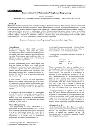
Transcription
Designing and BuildingTransistor Linear Power AmplifiersPart 2 — Apply techniques from Part 1 to single band HFand 6 meter linear amplifiers.Rick Campbell, KK7BInPart 1 of this series, Idescribed an experimental method fordesigning a linear amplifierstarting with a blank sheet ofpaper, some basic test equipment and an assortment of candidate transistors. In December2006 QST I described a singleband SSB exciter with 0 dBmoutput.1 An output level of0 dBm (1 mW) is very common for signal interconnections between 50 Ω blocks inradio systems. At this powerlevel, the SSB exciter outputmay be connected directly toan antenna for very low powerexperiments, it may be amplified to any desired output levelor it may be converted to adifferent frequency using amixer and VFO. It could alsobe connected to a simple RFclipper followed by a filter toobtain higher average-to-peakratio SSB, or it might even beconverted back down to theaudio range with a second oscillator for anumber of interesting analog signal processing applications. Several of these applications are illustrated in Figure 1.How Much Power do We Need?Once the signal has been moved aroundand processed at the 0 dBm power leveland is at the desired output frequency, mostapplications will require more power. If0.25 W is enough, then the amplifierdescribed in Experimental Methods in RFDesign, Figure 2.93 and included in theDecember 2006 QST article is highly recommended.2 Many on-air contacts have beenmade at that power level over remarkabledistances when band conditions enhance the1Notesappear at the end of the article.20 times (13 dB) more power,even in a low power (QRP)contest. One more stage ofamplification added to the0.25 W amplifier can overcomethat 13 dB difference. The5 to 10 W output level is acommon standard for portableradios with many commerciallyavailable examples.Putting Power in theAntennaFigure 2 is the block diagramof an experimental single-band36 dB gain 5 W linear amplifierthat may be easily constructedusing whatever output device isavailable. Two noteworthy differences between Figure 2 andother commonly published circuits are the use of a resistiveattenuatorand low-pass filterFigure 1 —between the driver and finalSome MicroT2applications.stage, and the floating groundat the final amplifier device.These two features make it easyto experiment with differenttransmitted signal and noise and interfer- final amplifier transistors without mechanience are low at the receiver. I’ve played that cal headaches or oscillations.game, and every contact entered into the logFigure 3 is the schematic of a 7 MHzis cause for a little celebration. But the bands version of the amplifier.1 It was optimized toare not always kind and high levels of noise use common, inexpensive ( 0.79) switchingand interference are common. You may power supply transistors. Since the 2N5739clearly hear the station on the other end of is not designed as an RF device, there arethe contact but he is probably running at least no suggested RF operating conditions inFigure 2 — A 37 dB gain linear amplifier.
the data sheet. The operating conditions rying much about burning out the device. Give Me Powerwere obtained experimentally by vary- I also varied the base bias, and changedThe collector power supply for the outputing the supply voltages while watching the drive level with a step attenuator. As stage is a common circuit, with a big capacithe output waveforms. The values of the expected, increased collector voltage made tor instead of the expected three terminalπ attenuators between stages were selected a big improvement in the linearity of strong regulator. That gives me about 18 V openexperimentally for best gain and distor- signals. Increased base bias improved the circuit, and about 16 V at maximum output.tion distribution among the three amplifier linearity of small signals.The big capacitor is split in two. The littlestages. The single-section low-pass filter onSince 100% modulated AM, SSB and box on the floor holds 2200 µF while anotherthe output of the driver transistor made a sig- two-tone outputs vary from some peak volt- 3500 µF is in the box with the speaker, varinificant reduction in high-order intermodu- age all the way to zero, both collector supply able bias supply, TR relay and 12 V threelation products, and seemed to improve the voltage and base bias determine the linearity terminal regulator. The regulator suppliessymmetry of the intermodulation distortion of the output. Each can also be used to destroy regulated voltage to the receiver, transmitterproducts as well.the device. Too much collector voltage will and other amplifier stages.burn out the transistor directly (rememberThe big capacitor provides the lowTweaking it into Submissionthat the voltage at the collector will generally impedance at audio needed in a SSB linearFigure 4 is the single-tone output spec- swing to significantly higher than twice the amplifier. By splitting it in two all of thetrum of the exciter driving the amplifier in supply voltage, even in a linear amplifier). components in the power supply and regulaFigure 3 with the two-tone output spectrum Too much base bias will either destroy the tor circuitry are physically and electricallyshown in Figure 5. Excellent linearity was transistor quickly as it conducts too much close to a big reservoir capacitor. Keepingobtained at a PEP output level of several collector current and overheats, or slowly as power supply lines clean is particularlywatts.the base-emitter junction warms up and the important around receivers. It is a simpleSince the amplifier is experimental and device goes into thermal runaway. I enjoyed power supply for an inexpensive transistor,the parts are inexpensive, I adjusted the col- exploring these options in the design phase and any efficiency I would have gained bylector supply voltage on the output stage of this amplifier, but have not burned out a using an expensive 13.8 V linear RF powerup and down and observed the impact on device since selecting the component values transistor in one of Granberg’s wonderfullyAM and two-tone waveforms without wor- and supply voltages shown in Figure 3.engineered circuits is more than offset byFigure 3 — 7 MHz linear amplifier based on inexpensive active devices.
QS0903-Campbell040-10-10-20-20-30-30-40-40dB -50dB 00Hz from Carrier Frequency10,00012,000Figure 4 — 7.165 MHz LSB single-tone output spectrum at 1 W(black) and 3 W (red) output. The desired LSB output tone is at3.7 kHz and the carrier is at 5.0 kHz on this display at about42 dB below the 1 W tone. Note suppressed upper sidebandtones at 6.3 kHz and unsuppressed modulator harmonicdistortion on upper sideband between about 9 kHz.QS0903-Campbell05002000400060008000Hz from Carrier Frequency10,00012,000Figure 5 — 7.165 MHz LSB two-tone output spectrum at 1 W(black) and 4 W (red) output. The carrier is at 5.0 kHz on thisdisplay at about 42 dB below the 1 W tone. Note that thirdorder products near the desired two-tone output increase by3 dB for each 1 dB increase in output power level. Also notethe unsuppressed modulator harmonic distortion on the uppersideband between 8 and 9 kHz.eliminating the series regulator. For morepower, I’ll experiment with operating thetransistor closer to its breakdown limits. Idon’t mind burning out a few output transistors during these experiments, because thetransistor is easy to change and costs lessthan a cup of coffee.Construction TechniquesFigure 6 is a photograph of the bias control supply and TR switching. The meterreads current in the final transistor whilethe knob below the meter is used to set thequiescent (no signal) bias level. The powertransformer was mounted where the speakeris now, but after a few experiments withmagnetic shielding to eliminate residualhum in the companion MicroR2 receiver, Istopped fighting basic physics and cured theproblem by putting the power transformer,rectifier and half of the capacitance in a boxon the floor.3 This ancient cure, adoptedlong ago, was once common with sensitivereceivers, and is still standard practice forsensitive audio and scientific instruments.After I removed the power transformer,I encountered another fringe benefit: anysource of 18 V dc will now power the wholetransceiver. Twelve AA cells in series willrun the receiver for days as well as powerintermittent SSB transmitting for 4 hoursor so.Putting the MicroT2 on 6 MetersThe fundamental crystal oscillator in theMicroT2 won’t go above about 25 MHz withcommon crystals, so another approach mustbe used for the bands above 12 meters. Theancient lore suggests frequency multipliers,and that approach was chosen for simplicity.Two 6 meter exciters were built, one with aFigure 6 — Classic 40 meter solid state QRP SSB station.16.7 MHz crystal oscillator and tripler, and theother with an 8.35 MHz oscillator, tripler anddoubler. An assortment of different crystalswas ordered from several different vendors,including Peterson Radio and International.The variable crystal oscillator (VXO) and 6 multiplier schematic are shown inFigure 7. The VXO circuit is the originalcircuitry in the MicroT2 circuit. The onlychange from the values in the original 40meter VXO described in QST is the valueof the low pass output transformer. This wascalculated using the formulas in QST andThe 2009 ARRL Handbook.4,5The 3 and 2 frequency multipliers werebuilt on a scrap of unetched copperclad board,using ugly construction. If using ugly construction at VHF, it is important to sketch thelayout first and think about which leads needto be short and which ones can be longer.The output of the doubler is about 1 mWat 50 MHz, with all spurs suppressed atleast 45 dB below the desired output. Thesespurs are further suppressed by the tunedFigure 7 — Prototype6 meter VXO triplerand doubler. Notethe short leads,gimmick capacitorsand symmetry in thelayout. Such circuitryis common on the lowVHF bands, and worksexceptionally well.The schematic is onthe gollowing page.
scraps left on bench Prototype version with VXO on same PC board. Thereare some minor circuitdifferences. Rick CampbellKK7B November 2007 Prototype veThere are so
Figure 8 — Schematic of 6 meter amplifier.Figure 9 —Photograph ofthe 6 meter 5 WSSB transmitter.The MicroT2 with 6 exciter is inthe black diecastbox in the lowerright. The VXOknob is in themiddle, and theMIC connectoron the right. Thecrystal socket onthe front panelis a mistake— the crystalbelongs insidethe box whereit is thermallyand electricallyshielded.RF amplifier in the MicroT2, and by thenarrow-band interstage tuning networksin the linear amplifier. The tuned doubleroutput drives the original MicroT2 bufferamplifier circuit. The only other changeto the MicroT2 is retuning the RF amplifier output to 50 MHz. That may be easilydone by changing MicroT2 L3 to 16 turnson a T25-6 ferrite toroid, changing C21 toa 20 pF trimmer, and leaving C20 out of thecircuit. If the MicroT2 RF amplifier stage isbuilt using ugly construction, short leads arenecessary, particularly for connections to thegate of Q6.Experiments with running the TUF-3mixers as third harmonic mixers with directIQ LO drive at 16.7 MHz were initiallyencouraging, with very good carrier suppression at 50 MHz, but distortion was high.A very simple rig could be built with thatapproach.The 8 MHz crystal from Internationalin the large can provides a very stable frequency tuning range of about 50 kHz on6 meters, over the useful range from50.115 to 50.165 MHz. The 16.7 MHz crystal and tripler provides a narrower range,
QS0903-Campbell110-10-10-20-20-30-30-40-40dB -50dB 00Hz from Carrier FrequencyMicroT2 1 tone10,00012,000Icom 502 1 toneFigure 10 — MicroT2 and PA 50.125 MHz single-tone USBoutput spectrum compared with ICOM IC-502 single-tone outputspectrum. In each case the suppressed carrier is at 5500 Hz onthis plot. The '502 output is about 0.5 W and the MicroT2 and PA isat about 5 W output. Carrier suppression and opposite sidebandsuppression are not as good with the MicroT2, but in-channeldistortion is lower, even if the ’502 is backed off 8 dB from itsrated output.QS0903-Campbell12002000400060008000Hz from Carrier FrequencyMicroT2 2 tone10,00012,000Icom 502 2 toneFigure 11 — MicroT2 and PA 50.125 MHz two-tone USB outputspectrum (black) compared with IC-502 two-tone outputspectrum (red). In each case the suppressed carrier is at 5500 Hzon this plot. The '502 output is about 1 W PEP and the MicroT2and PA is at about 5 W PEP output. Carrier suppression andopposite sideband suppression are not as good with the MicroT2,but in-channel distortion is lower, even when the '502 is backedoff 5 dB from its rated output.Figure 10 is the single-tone output specure 8, which is used on both the driver andfinal. The MRF 134 and 136 have enough trum at the 5 W level, compared with thegain at 50 MHz that two stages are sufficient output of a commercial radio in the sameto amplify the output of the MicroT2 exciter power class. Note that the carrier level isto the 5 W level. Figure 9 is a photograph higher than we would like, at only aboutof the 6 meter amplifier connected to the 33 dB below the peak output power. The6 meter exciter with MicroT2 exciter and 6 two-tone spectrum shown in Figure 11 ismultiplier. This amplifier is simply the pack- certainly good enough to use on the air. Aaged up version of the amplifier I tested on comparison between the spectra of thesethe bench. It is still a work in progress. Note two rigs on 6 meters illustrates a commonhow easily the final output transistor may be difference between phasing and filter SSBchanged to a different FET, or even a bipolar transmitters. Phasing rigs have lower distortion in-channel, so they sound very good, buttransistor.The 6 Meter AmplifierEach modular section of the 6 meter filter rigs have fewer off-channel spuriousThe 2SC5739 transistor has low gain at transmitter is separate, including the bias Ts outputs.This 6 meter SSB signal sounds excep50 MHz, so different driver and final devices described in Part 1 and the output networks.were chosen for the 6 meter linear amplifier. The bias networks and low-pass filter are on tional on the air, and the carrier could beIn keeping with the experimental nature of separate boards. This makes it very easy to acquired and locked by a phase locked loopthe project, both of these devices came from measure, adjust and modify any part of the (PLL) for a signal with the fidelity of the bestthe junk box, in fact they were unsoldered circuit, or insert additional gain or attenu- AM signal, at a fraction of the bandwidthfrom a printed circuit (PC) board obtained ation anywhere. All of the pieces except and total radiated power. There is room forat a flea market. The driver transistor is an the black diecast box are from the author’s experiments with such modes on the VHFMRF134, and the final is a MRF136 power junk box, including the thick aluminum and UHF bands.My personal choice is to use phasing forFET unsoldered from an old PC board. The plates used for heat sinks. Even the MicroT2MRF136 is capable of much more power exciter was pieced together from prototype QRP SSB rigs and VHF-UHF SSB, wherethe off-channel products don’t generallyoutput than the 2SC5739, so a larger heat modules from the MicroT2 project.The plethora of 2200 µF, 50 V electro- bother anyone. For high power operationsink was used. The bias connection is different as well, since the FETs require forward lytics will continue until that bag is empty. on crowded HF bands, I follow the phasingbias of about 4 V on the gate. These small Because this transmitter was assembled at exciter with a crystal filter and heterodynevariations are easily seen in the schematic low cost from the available ingredients, I system.refer to it as the “Blue Plate Special.” Theof Figure 8.The performance of the broadband 4PDT relay in the lower right corner is the Checking it TwiceThe procedure I use for a quick check4:1 bias T described in Part 1 degrades TR relay, and includes an RF output andabove 35 MHz, and with a 28 V supply, a muting to the receiver and 6 meter converter. of amplifier performance before putting a12.5 Ω load impedance is too low for a 5 W The set of contacts next to the ground plane signal on the air is very different from theclass amplifier. A quick search of the junk are used for the 6 meter RF, an additional measurements and experiments I use tobox and a few minutes with a Smith Chart shield was added, and RF connections to the design an amplifier. With these amplifiers,I connect a dummy load and wattmeter toresulted in the output network seen in Fig- relay are made with small diameter coax.about 35 kHz. These are observations witha sample size of one, so I hesitate to drawany firm conclusions. One observation isthat the carrier suppression improves whenthe cans of the TUF-3 mixers are soldered tothe circuit board all the way around. This isprevented by solder mask on the current production circuit boards, but it is a worthwhilemodification. For much better carrier suppression, wider tuning range and transceiveoperation, a heterodyne approach from alower frequency is recommended.
the output of the low-pass filter, and drive ment, it’s a choice, and in many cases it willthe amplifier chain to saturation with a get through when nothing else will. SSB isCW signal. I observe the current drain at this nice for casual conversations, digital modessaturated output level, and then set the rest- are wonderful if you don’t mind sharing theing bias to about one tenth that level. These fun with a computer, but CW is simple and5 W amplifiers idle at around 100 mA, so the power advantage on transmit is only partthat is 1.8 W for the 7 MHz amplifier and of the equation.2.7 W for the 6 meter version. Then I speakThe linear amplifiers described in thisinto the microphone and observe that the article are remarkable in two ways:output peaks are about 3 dB below the satu The experimental design procedurerated CW output level. That results in a very provides a real education in linear amplinice sounding signal on the air.fier design, measurement, adjustment andIf you have been doing the math, you construction.can quickly estimate that my average output They were designed around the devicespower on SSB ends up being about one tenth on hand, and built at nearly zero cost.the saturated CW output power. PEP outputIn that sense, they follow the best tradicapability is considerably higher than the tions of the Amateur Radio service and innoaverage, but I prefer natural sounding SSB vative design engineering.to the highly processed sound that results inan average power output very close to the 1NotesR. Campbell, KK7B, “The MicroT2 — APEP output capability of the amplifier. ThisCompact Single-Band SSB Transmitter,”is personal preference, and directly relatedQST, Dec 2006, pp 28-33.2W. Hayward, W7ZOI, R. Campbell, KK7B, andto my willingness to switch to CW when sigB. Larkin, W7PUA, Experimental Methods innals are marginal. CW is no longer a requireRF Design. Available from your ARRL dealeror the ARRL Bookstore, ARRL order no.8799. Telephone 860-594-0355, or toll-free inthe US 888-277-5289; www.arrl.org/shop;pubsales@arrl.org.3R. Campbell, KK7B, “The MicroR2 — An Easyto Build ‘Single Signal’ SSB or CW Receiver,”QST, Oct 2006, pp 28-33.4The ARRL Handbook for Radio Communications, 2009 Edition. Available from your ARRLdealer or the ARRL Bookstore, ARRL orderno. 0261 (Hardcover 0292). Telephone860-594-0355, or toll-free in the US888-277-5289; www.arrl.org/shop;pubsales@arrl.org.5This circuitry is nearly identical to the circuitused for the 40 meter version, and can usethe same circuit traces. The output may betaken from MicroT2 C41 by leaving R59, 60and 61 off the circuit board. The VHF uglyconstructed tripler and doubler circuitry isinserted in the MicroT2 circuit in place ofR60. Short small diameter coax or twistedpair should be used for the interconnections.This circuitry should be shielded from theRF output amplifier to improve carrier suppression.See Part 1 for Rick’s biography. You can contact Rick at 4105 NW Carlton Ct, Portland,OR 97229, or at kk7b@hotmail.com.
Designing and Building Transistor Linear Power Amplifiers Part 2 — Apply techniques from Part 1 to single band HF and 6 meter linear amplifiers. Rick Campbell, KK7B 1Notes appear at the end of the article. Figure 2 — A 37 dB gain linear amplifier. Figure 1 — Some MicroT2