Transcription
Freescale SemiconductorData Sheet: Technical DataDocument Number: MC13783Rev. 3.5, 7/2009MC13783Package InformationPlastic Package10 10 mm packageMC13783Power Management andAudio Circuit1IntroductionThe MC13783 is a highly integrated power managementand audio component dedicated to handset and portableapplications covering GSM, GPRS, EDGE, and UMTSstandards. The MC13783 implements high-performanceaudio functions suited to high-end applications such assmartphones and UMTS handsets.Ordering InformationDeviceDevice Marking orOperatingTemperature RangePackageMC13783–30 to 85 CMAPBGA-247Contents123456Introduction . . . . . . . . . . . . . . . . . . . . . . . . . . 1Signal Descriptions . . . . . . . . . . . . . . . . . . . . 6Electrical Characteristics . . . . . . . . . . . . . . 16Functional Description . . . . . . . . . . . . . . . . 17Package Information . . . . . . . . . . . . . . . . . . 47Product Documentation . . . . . . . . . . . . . . . . 48The MC13783 provides the following key benefits: Full power management and audio functionalityin one module optimizes system size. High level of integration reduces the powermanagement and audio system bill of materials. Versatile solution offers large possibilities offlexibility through simple programming (64registers of 24-bit data). Implemented DVS saves significant batteryresources in every mode (compatibility with alarge number of processors). Dual channel voice ADC improves intelligibility.Freescale reserves the right to change the detail specifications as may be required to permit improvements in the design of itsproducts. Freescale Semiconductor, Inc., 2005–2009. All rights reserved.
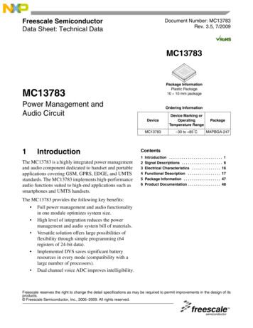
IntroductionThe detailed block diagram of the MC13783 in Figure 1 shows the wide functionality of the MC13783,including the following features: Battery charger interface for wall charging and USB charging 10 bit ADC for battery monitoring and other readout functions Buck switchers for direct supply of the processor cores Boost switcher for backlight and USB on the go supply Regulators with internal and external pass devices Transmit amplifiers for two handset microphones and a headset microphone Receive amplifiers for earpiece, loudspeaker, headset and line out 13 bit Voice CODEC with dual ADC channel and both narrow and wide band sampling 13 bit Stereo recording from an analog input source such as FM radio 16 bit Stereo DAC supporting multiple sample rates Dual SSI audio bus with network mode for connection to multiple devices Power control logic with processor interface and event detection Real time clock and crystal oscillator circuitry Dual SPI control bus with arbitration mechanism Multiple backlight drivers and LED control including funlight support USB FS/LS transceiver with OTG and CEA-936-A Carkit support Touchscreen interfaceThe main functions of the MC13783 are described in the following sections. A detailed block diagram isshown in Figure 1, on page 3.MC13783 Technical Data, Rev. 3.52Freescale Semiconductor
NDSUB8REFDREFCREFBREFAGNDATLASVATLASTri-ColorLED DriveBacklightLED 0CHRGMOD1CHRGRAWCharger Interface and Control:4 bit DAC, Clamp, Protection,Trickle GenerationBattery Interface BPBATTFETBATTBATTISNSIntroductionPWRGateDrive& ChgPumpAudioReferencesVATLASGenFrom Li CellVoltage /CurrentSensing IN9ADIN10ADIN11Thermal WarningDetectionTo InterruptSectionA/D ResultA/DControl10 BitMUXTriggerHandlingA/DTouchBUCK 1A500 mAO/PDriveSW1AINSW1AOUTGNDSW1ASW1AFBBUCK 1B500 mAO/PDriveSW1BINSW1BOUTGNDSW1BSW1BFBBUCK 2A500 mAO/PDriveBUCK2B500 mAO/PDriveBOOST350 mAO/PDriveLOBATBP IGPRIVCCA/D ResultToInterruptSectionLDO Monitoringand EOLDetectionLDOsScreenInterfaceShift RegisterPRICSPRICLKPrimaryPRIMOSIInterfacePrimary SPIConfigRegSPICombinational LogicSECCSSECCLKSECMOSISECMISOGNDSPIMC2B4Shift RegisterRegistersPRIMISOSECVCCResult RegistersTo Core LogicSPISecondary SPIInterfaceRbiasRbiasMC1LBRbiasShift INRegistersDetectPGAA to OLShift RegisterPGAD to assFETVINGENVGENVCAMPassFETVINCAMVCAM5Voice VRF2DRVVRF2LSPPPGAmSelectorAlspLSPMGNDLSPStereoD to nableControlPGAstAhslTo INLPLLLPFGNDPLLBPVBKUP1VBKUP2CSOUTPCUTPLL32x ECSTANDBYPRIVBUS5VPassFETVUSB3.3VPassFETUSB/RS-232 BusGNDCTRLTo Interrupt Section USB On-The-GoSPARE4VBUS32 kHzBufferVINBUSEnables &ControlVUSBInterruptInputsCore Control Logic, Timers, & AL1GNDRTCGNDAUD4GNDAUD5GNDAUD3GNDAUD2Li CellChargerUSB Car Kit DetectSPI ResultRegisters32 kHzCrystalOscCLIBTo Charger 32 CL1GPO2PWRFAILPowerFailDetectTo VESIMFrom TXOUTTX1SW2BINSW2BOUTGNDSW2BSW2BFBVAUDIOA to WGT2ENPWGT2DRVFigure 1. MC13783 Detailed Block DiagramMC13783 Technical Data, Rev. 3.5Freescale Semiconductor3
Introduction1.1AudioThe audio section is composed of microphone amplifiers and speaker amplifiers, a voice CODEC, and astereo DAC.Three microphone amplifiers are available for amplification of two handset microphones and of theheadset microphone. The feedback networks are fully integrated for a current input arrangement. A lineinput buffer amplifier is provided for connecting external sources. All microphones have their ownstabilized supply with an integrated microphone sensitivity setting. The microphone supplies can bedisabled. The headset microphone supply has a fully integrated microphone detection.Several speaker amplifiers are provided. A bridged earpiece amplifier is available to drive an earpiece.Also, a battery supplied bridged amplifier with thermal protection is included to drive a low ohmic speakerfor speakerphone and alert functionality. The performance of this amplifier allows it to be used as well forearpiece drive to support applications with a single transducer combining earpiece, speakerphone and alertfunctionality, thus avoiding the use of multiple transducers.A left audio out is provided which in combination with a discrete power amplifier and the integratedspeaker amplifier allows for a stereo speaker application. Two, single-ended amplifiers are included for thestereo headset drive including headset detection. The stereo headset return path is connected to a phantomground which avoids the use of large DC decoupling capacitors. The additional stereo receive signaloutputs can be used for connection to external accessories like a car kit. Via a stereo line in, externalsources such as an FM radio or standalone midi ringer can be applied to the receive path.A voice CODEC with a dual path ADC is implemented following GSM audio requirements. Both narrowband and wide band voice is supported. The dual path ADC allows for conversion of two microphonesignal sources at the same time for noise cancellation or stereo applications as well as for stereo recordingfrom sources like FM radio. A 16-bit stereo DAC is available which supports multi-clock modes. Anon-board PLL ensures proper clock generation. The voice CODEC and the stereo DAC can be operated atthe same time via two interchangeable buses supporting master and slave mode, network mode, as well asthe different protocols like I2S.Volume control is included in both transmit and receive paths. The latter also includes a balance controlfor stereo. The mono adder in the receive path allows for listening to a stereo source on a mono transducer.The receive paths for stereo and mono are separated to allow the two sources to be played backsimultaneously on different outputs. The different sources can be analog mixed and two sources on the SSIconfigured in network mode can be mixed as well.1.2Switchers and RegulatorsThe MC13783 provides most of the telephone reference and supply voltages.Four down converters and an up converter are included. The down, or buck, converters provide the supplyto the processors and to other low voltage circuits such as IO and memory. The four down converters canbe combined into two higher power converters. Dynamic voltage scaling is provided on each of the downconverters. This allows under close processor control to adapt the output voltage of the converters tominimize processor current drain. The up, or boost, converter supplies the white backlight LEDs and theMC13783 Technical Data, Rev. 3.54Freescale Semiconductor
Introductionregulators for the USB transceiver. The boost converter output has a backlight headroom tracking optionto reduce overall power consumption.The regulators are directly supplied from the battery or from the switchers and include supplies for IO andperipherals, audio, camera, multi media cards, SIM cards, memory and the transceivers. Enables forexternal discrete regulators are included as well as a vibrator motor regulator. A dedicated preamplifieraudio output is available for multifunction vibrating transducers.Drivers for power gating with external NMOS transistors are provided including a fully integrated chargepump. This will allow to power down parts of the processor to reduce leakage current.1.3Battery ManagementThe MC13783 supports different charging and supply schemes including single path and serial pathcharging. In single path charging, the phone is always supplied from the battery and therefore always hasto be present and valid. In a serial path charging scheme, the phone can operate directly from the chargerwhile the battery is removed or deeply discharged.The charger interface provides linear operation via an integrated DAC and unregulated operation like usedfor pulsed charging. It incorporates a standalone trickle charge mode in case of a dead battery with LEDindicator driver. Over voltage, short circuit and under voltage detectors are included as well as chargerdetection and removal. The charger includes the necessary circuitry to allow for USB charging and forreverse supply to an external accessory. The battery management is completed by a battery presencedetector and an A to D converter that serves for measuring the charge current, battery and other supplyvoltages as well as for measuring the battery thermistor and die temperature.1.4LogicThe MC13783 is fully programmable via SPI bus. Additional communication is provided by direct logicinterfacing. Default startup of the device is selectable by hard-wiring the power up mode select pins.Both the call processor and the applications processor have full access to the MC13783 resources via twoindependent SPI busses. The primary SPI bus is able to allow the secondary SPI bus to control all or someof the registers. On top of this an arbitration mechanism is built in for the audio, the power and ADCfunctions. This together will avoid programming conflicts in case of a dual processor type of application.The power cycling of the phone is driven by the MC13783. It has the interfaces for the power buttons anddedicated signaling interfacing with the processor. It also ensures the supply of the memory and othercircuits from the coin cell in case of brief power failures. A charger for the coin cell is included as well.Several pre-selectable power modes are provided such as SDRAM self refresh mode and user off mode.The MC13783 provides the timekeeping based on an integrated low power oscillator running with astandard watch crystal. This oscillator is used for internal clocking, the control logic, and as a referencefor the switcher PLL. The timekeeping includes time of day, calendar and alarm. The clock is put out tothe processors for reference and deep sleep mode clocking.MC13783 Technical Data, Rev. 3.5Freescale Semiconductor5
Signal Descriptions1.5Miscellaneous FunctionsThe drivers and comparators for a USB On-the-Go and a CEA-936-A compatible USB carkit includingaudio routing, as well as RS232 interfaces are provided. Special precautions are taken to allow for specificbooting and accessory detection modes.Current sources are provided to drive tricolored funlights and signaling LEDs. The funlights havepreprogrammed lighting patterns. The wide programmability of the tricolored LED drivers allows forapplications such as audio modulation. Three backlight drivers with auto dimming are included as well forkeypad and dual display backlighting.A dedicated interface in combination with the A to D converter allow for precise resistive touchscreenreading. Pen touch wake up is included.2Signal DescriptionsThe below pinout description gives the pin name per functional block with its row-column coordinates, itsmaximum voltage rating, and a functional description.Table 1. Pinout HV1. Charger input2. Output to battery supplied accessoriesCHRGCTRLC18EHVDriver output for charger path FETs M1 and M2BPFETB15EHV1. Driver output for dual path regulated BP FET M42. Driver output for separate USB charger path FETs M5 and M6CHRGISNSPB17MVCharge current sensing point 1CHRGISNSNC14MVCharge current sensing point 2BPB13MV1. Application supply point2. Input supply to the MC13783 core circuitry3. Application supply voltage senseBATTFETA12MVDriver output for battery path FET M3BATTISNSA14MVBattery current sensing point 1BATTD15MV1. Battery positive terminal2. Battery current sensing point 23. Battery supply voltage senseCHRGMOD0D17LVSelection of the mode of chargingCHRGMOD1A16LVSelection of the mode of chargingCharger* The maximum voltage rating is given per category of pins: EHV for Extended High Voltage (20 V) HV for High Voltage (7.5 V) EMV for Extended Medium Voltage (5.5 V) MV for Medium Voltage (4.65 V) LV for Low Voltage (3.1 V)MC13783 Technical Data, Rev. 3.56Freescale Semiconductor
Signal DescriptionsTable 1. Pinout Listing CHRGLEDD13EHVGNDCHRGJ11—LEDMD1B8EMVMain display backlight LED driver output 1LEDMD2F9EMVMain display backlight LED driver output 2LEDMD3E9EMVMain display backlight LED driver output 3LEDMD4C9EMVMain display backlight LED driver output 4LEDAD1C8EMVAuxiliary display backlight LED driver output 1LEDAD2E8EMVAuxiliary display backlight LED driver output 2LEDKPC7EMVKeypad lighting LED driver outputLEDR1B10EMVTricolor red LED driver output 1LEDG1E11EMVTricolor green LED driver output 1LEDB1F11EMVTricolor blue LED driver output 1LEDR2E10EMVTricolor red LED driver output 2LEDG2F10EMVTricolor green LED driver output 2LEDB2G10EMVTricolor blue LED driver output 2LEDR3F8EMVTricolor red LED driver output 3LEDG3C10EMVTricolor green LED driver output 3LEDB3B9EMVTricolor blue LED driver output 3GNDLEDBLH10—Ground for backlight LED driversGNDLEDTCJ10—Ground for tricolor LED driversVATLASC12LVRegulated supply output for the MC13783 core circuitryREFATLASB11LVMain bandgap referenceGNDATLASH11—Ground for the MC13783 core circuitrySW1AINK18MVSwitcher 1A inputSW1AOUTK17MVSwitcher 1A outputSW1AFBL18LVSwitcher 1A feedbackCharger forced SE1 detection inputTrickle LED driver outputGround for charger interfaceLED DriversMC13783 CoreSwitchers* The maximum voltage rating is given per category of pins: EHV for Extended High Voltage (20 V) HV for High Voltage (7.5 V) EMV for Extended Medium Voltage (5.5 V) MV for Medium Voltage (4.65 V) LV for Low Voltage (3.1 V)MC13783 Technical Data, Rev. 3.5Freescale Semiconductor7
Signal DescriptionsTable 1. Pinout Listing ynamic voltage scaling logic input for switcher 1AGNDSW1AL17—Ground for switcher 1ASW1BINN18MVSwitcher 1B inputSW1BOUTN17MVSwitcher 1B outputSW1BFBM18LVSwitcher 1B feedbackDVSSW1BK15LVDynamic voltage scaling logic input for switcher 1BGNDSW1BM17—Ground for switcher 1BSW2AINP18MVSwitcher 2A inputSW1ABSPBP11LVSW1 mode configurationSW2AOUTR18MVSwitcher 2A outputSW2AFBP15LVSwitcher 2A feedbackDVSSW2AH15LVDynamic voltage scaling logic input for switcher 2AGNDSW2AP17—Ground for switcher 2ASW2BINU18MVSwitcher 2B inputSW2BOUTT18MVSwitcher 2B outputSW2BFBR17LVSwitcher 2B feedbackDVSSW2BJ14LVDynamic voltage scaling logic input for switcher 2BGNDSW2BT17—Ground for switcher 2BSW2ABSPBR12LVSW2 mode configurationSW3INJ17HVSwitcher 3 inputSW3OUTH18HVSwitcher 3 outputSW3FBH17HVSwitcher 3 feedbackGNDSW3J18—Ground for switcher 3PWGT1ENL14LVPower gate driver 1 enablePWGT1DRVM15EMVPower gate driver 1 outputPWGT2ENL15LVPower gate driver 2 enablePWGT2DRVK14EMVPower gate driver 2 outputU12MVPower GatingRegulatorsVINAUDIOInput regulator audio* The maximum voltage rating is given per category of pins: EHV for Extended High Voltage (20 V) HV for High Voltage (7.5 V) EMV for Extended Medium Voltage (5.5 V) MV for Medium Voltage (4.65 V) LV for Low Voltage (3.1 V)MC13783 Technical Data, Rev. 3.58Freescale Semiconductor
Signal DescriptionsTable 1. Pinout Listing tput regulator audioVINIOLOU13MVInput regulator low voltage IOVIOLOV13LVOutput regulator low voltage IOVINIOHIB7MVInput regulator high voltage IOVIOHIB6LVOutput regulator high voltage IOVINDIGR11MVInput regulator general digitalVDIGU11LVOutput regulator general digitalVINRFDIGK5MVInput regulator transceiver digitalVRFDIGK2LVOutput regulator transceiver digitalVINRFREFK7MVInput regulator transceiver referenceVRFREFG3LVOutput regulator transceiver referenceVRFCPG2LVOutput regulator transceiver charge pumpVRFBGC11LVBandgap reference output for transceiverVINSIMF2MVInput regulator SIM card and eSIM cardVSIME3LVOutput regulator SIM cardVESIMF3LVOutput regulator eSIM cardVINVIBG5MVInput regulator vibrator motorVVIBE2LVOutput regulator vibrator motorVINGENG17MVInput regulator graphics acceleratorVGENG18LVOutput regulator graphics acceleratorVINCAMV12MVInput regulator cameraVCAMV11LVOutput regulator cameraVRF2DRVJ6MVDrive output regulator transceiverVRF2J5LVOutput regulator transceiverVRF1DRVK8MVDrive output regulator transceiverVRF1J3LVOutput regulator transceiverVMMC1DRVL7MVDrive output regulator MMC1 moduleVMMC1K6LVOutput regulator MMC1 moduleVMMC2DRVJ2MVDrive output regulator MMC2 moduleVMMC2K3LVOutput regulator MMC2 module* The maximum voltage rating is given per category of pins: EHV for Extended High Voltage (20 V) HV for High Voltage (7.5 V) EMV for Extended Medium Voltage (5.5 V) MV for Medium Voltage (4.65 V) LV for Low Voltage (3.1 V)MC13783 Technical Data, Rev. 3.5Freescale Semiconductor9
Signal DescriptionsTable 1. Pinout Listing M enable inputESIMENF16LVVESIM enable inputVIBENE19LVVVIB enable inputREGENE18LVRegulator enable inputGPO1G8LVGeneral purpose output 1 to be used for enabling a discrete regulatorGPO2F6LVGeneral purpose output 2 to be used for enabling a discrete regulatorGPO3E5LVGeneral purpose output 3 to be used for enabling a discrete regulatorGPO4G9LVGeneral purpose output 4 to be used for enabling a discrete regulatorGNDREG1N12—Ground for regulators 1GNDREG2K10—Ground for regulators 2UDPC2EMV1. USB transceiver cable interface, D 2. RS232 transceiver cable interface, transmit output or receive input signalUDMD2EMV1. USB transceiver cable interface, D2. RS232 transceiver cable interface, receive input or transmit output signalUIDF7EMVUSB on the go transceiver cable ID resistor connectionUDATVPC5LV1. USB processor interface transmit data input (logic level version of D /D-) ortransmit positive data input (logic level version of D )2. Optional USB processor interface receive data output (logic level version of D /D-)3. RS232 processor interfaceUSE0VMC6LV1. USB processor interface transmit single ended zero signal input or transmit minusdata input (logic level version of D-)2. Optional USB processor interface received single ended zero output3. Optional RS232 processor interfaceUTXENBC4LV1. USB processor interface transmit enable barURCVDB5LVOptional USB receiver processor interface differential data output (logic level versionof D /D-)URXVPB3LVOptional USB receiver processor interface data output (logic level version of D )URXVMB2LV1. Optional USB receiver processor interface data output (logic level version of D-)2. Optional RS232 processor interfaceUMOD0H7LVUSB transceiver operation mode selection at power up 0UMOD1G6LVUSB transceiver operation mode selection at power up 1USBENC3LVBootmode enable for USB/RS232 interfaceVINBUSB4EMVUSB/RS232Input for VBUS and VUSB regulators for USB on the go mode* The maximum voltage rating is given per category of pins: EHV for Extended High Voltage (20 V) HV for High Voltage (7.5 V) EMV for Extended Medium Voltage (5.5 V) MV for Medium Voltage (4.65 V) LV for Low Voltage (3.1 V)MC13783 Technical Data, Rev. 3.510Freescale Semiconductor
Signal DescriptionsTable 1. Pinout Listing hen in common input configuration, shorted to CHRGRAW1. USB transceiver cable interface VBUS2. Output VBUS regulator in USB on the go modeWhen in separate input configuration, not shorted to CHRGRAW1. USB transceiver cable interface VBUS2. Output VBUS regulator in USB on the go modeVUSBF5MVOutput VUSB regulator as used by the USB transceiverUSBVCCE7LVSupply for processor interfaceGNDUSBAA1A2B1—Ground for USB transceiver and USB cableGNDUSBDK9—Ground for USB processor interfaceON1BE16LVPower on/off button connection 1ON2BE15LVPower on/off button connection 2ON3BG14LVPower on/off button connection 3WDIF17LVWatchdog inputRESETBG15LVReset outputRESETBMCUF18LVReset for the processorSTANDBYPRIH14LVStandby input signal from primary processorSTANDBYSECJ13LVStandby input signal from secondary processorLOBATBN14LVLow battery indicator signal or end of life indicator signalPWRRDYU17LVPower ready signal after DVS and power gate transitionPWRFAILF13LVPowerfail indicator output to processor or systemUSEROFFE14LVUser off signaling from processorMEMHLDDRVG12LVMemory hold FET drive for power cut supportCSOUTG11LVChip select output for memoryLICELLC16MV1. Coincell supply input2. Coincell charger outputVBKUP1E12LVBackup output voltage for memoryVBKUP2F12LVBackup output voltage for processor coreGNDCTRLJ12—Ground for control logicControl Logic* The maximum voltage rating is given per category of pins: EHV for Extended High Voltage (20 V) HV for High Voltage (7.5 V) EMV for Extended Medium Voltage (5.5 V) MV for Medium Voltage (4.65 V) LV for Low Voltage (3.1 V)MC13783 Technical Data, Rev. 3.5Freescale Semiconductor11
Signal DescriptionsTable 1. Pinout Listing (continued)PinLocationRating*FunctionOscillator and Real Time ClockXTAL1V16LV32.768 kHz Oscillator crystal connection 1XTAL2V14LV32.768 kHz Oscillator crystal connection 2CLK32KR14LV32 kHz Clock outputCLK32KMCUE13LV32 kHz Clock output to the processorCLKSELU16LVEnables the RC clock routing to the outputsGNDRTCV15—Ground for the RTC blockPUMS1H6LVPower up mode supply setting 1PUMS2J7LVPower up mode supply setting 2PUMS3H5LVPower up mode supply setting 3ICTESTF14LVTest mode selectionICSCANU14LVScan mode selectionPRIVCCN2LVSupply for primary SPI bus and audio bus 1PRICLKN5LVPrimary SPI clock inputPRIMOSIN8LVPrimary SPI write inputPRIMISOP7LVPrimary SPI read outputPRICSN6LVPrimary SPI select inputPRIINTP5LVInterrupt to processor controlling the primary SPI busSECVCCN3LVSupply for secondary SPI bus and audio bus 2SECCLKP6LVSecondary SPI clock inputSECMOSIR6LVSecondary SPI write inputSECMISOR5LVSecondary SPI read outputSECCSP8LVSecondary SPI select inputSECINTR7LVInterrupt to processor controlling the secondary SPI busGNDSPIL9LVGround for SPI interfaceBATTDETBK13LVBattery thermistor presence detect outputADIN5M14LVADC generic input channel 5, group 1Power Up SelectSPI InterfaceA to D Converter* The maximum voltage rating is given per category of pins: EHV for Extended High Voltage (20 V) HV for High Voltage (7.5 V) EMV for Extended Medium Voltage (5.5 V) MV for Medium Voltage (4.65 V) LV for Low Voltage (3.1 V)MC13783 Technical Data, Rev. 3.512Freescale Semiconductor
Signal DescriptionsTable 1. Pinout Listing (continued)PinLocationRating*FunctionADIN6U15LVADC generic input channel 6, group 1ADIN7R15LVADC generic input channel 7, group 1ADIN8P14LVADC generic input channel 8, group 2ADIN9V17LVADC generic input channel 9, group 2ADIN10V18LVADC generic input channel 10, group 2ADIN11V19W18W19LVADC generic input channel 11, group 2TSX1P13LVADC generic input channel 12 or touchscreen input X1, group 2TSX2L13LVADC generic input channel 13 or touchscreen input X2, group 2TSY1P12LVADC generic input channel 14 or touchscreen input Y1, group 2TSY2M13LVADC generic input channel 15 or touchscreen input Y2, group 2ADREFR13LVReference for ADC and touchscreen interfaceADTRIGN15LVADC trigger inputADOUTE6LVADC trigger outputGNDADCL12—Ground for A to D circuitryBCL1M7LVBit clock for audio bus 1. Input in slave mode, output in master modeFS1M9LVFrame synchronization clock for audio bus 1. Input in slave mode, output in mastermodeRX1L5LVReceive data input for audio bus 1TX1M6LVTransmit data output for audio bus 1BCL2M8LVBit clock for audio bus 2. Input in slave mode, output in master modeFS2M2LVFrame synchronization clock for audio bus 2. Input in slave mode, output in mastermodeRX2M3LVReceive data input for audio bus 2TX2M5LVTransmit data output for audio bus 2CLIAL6LVClock input for audio bus 1 or 2CLIBL3LVClock input for audio bus 1 or 2MC1RBR2LVHandset primary or right microphone supply output with integrated bias resistorMC1LBP3LVHandset secondary or left microphone supply output with integrated bias resistorAudio BusAudio Transmit* The maximum voltage rating is given per category of pins: EHV for Extended High Voltage (20 V) HV for High Voltage (7.5 V) EMV for Extended Medium Voltage (5.5 V) MV for Medium Voltage (4.65 V) LV for Low Voltage (3.1 V)MC13783 Technical Data, Rev. 3.5Freescale Semiconductor13
Signal DescriptionsTable 1. Pinout Listing et microphone supply output with integrated bias resistor and detectMC1RINV2LVHandset primary or right microphone amplifier inputMC1LINU2LVHandset secondary or left microphone amplifier inputMC2INU3LVHeadset microphone amplifier inputTXINU4LVGeneral purpose line level transmit inputTXOUTV3LVBuffered output of CEA-936-A microphone signalSPPV9LVHandset earpiece speaker amplifier output positive terminalSPMV10LVHandset earpiece speaker amplifier output minus terminalVINLSPV6MVHandset loudspeaker and alert amplifier supply inputLSPPV5MVHandset loudspeaker and alert amplifier positive terminalLSPMV4MVHandset loudspeaker and alert amplifier minus terminalGNDLSPV1W1W2—Ground for loudspeaker amplifierLSPLU5LVLow power output for discrete loudspeaker amplifier, associated to left channel audioCDCOUTU6LVLow power output for discrete amplifier, associated to voice CODEC channelHSLV8LVHeadset left channel amplifier outputHSRU9LVHeadset right channel amplifier outputHSPGFV7LVHeadset phantom ground power line (force)HSPGSP10LVHeadset phantom ground feedback line (sense)HSDETR10LVHeadset sleeve detection inputHSLDETR8LVHeadset left detection inputRXOUTRU7LVLow power receive output for accessories right channelRXOUTLP9LVLow power receive output for accessories left channelRXINRR9LVGeneral purpose receive input right channelRXINLU8LVGeneral purpose receive input left channelREFAR3LVReference for audio amplifiersREFBT3LVReference for low noise audio bandgapREFCT2LVReference for voice CODECAudio ReceiveAudio Other* The maximum voltage rating is given per category of pins: EHV for Extended High Voltage (20 V) HV for High Voltage (7.5 V) EMV for Extended Medium Voltage (5.5 V) MV for Medium Voltage (4.65 V) LV for Low Voltage (3.1 V)MC13783 Technical Data, Rev. 3.514Freescale Semiconductor
Signal DescriptionsTable 1. Pinout Listing ence for stereo DACPLLLPFH2LVConnection for the stereo DAC PLL low pass filter.GNDPLLH3—Dedicated ground for the stereo DAC PLL block.GNDAUD1L10—Ground for audio circuitry 1 (analog)GNDAUD2M10—Ground for audio circuitry 2 (analog)GNDAUD3M11—Ground for audio circuitry 3 (analog)GNDAUD4M12—Ground for audio circuitry 4 (digital)GNDAUD5H9—Ground for audio circuitry 5 (digital)GNDSUB1N11—Non critical signal ground and thermal heatsinkGNDSUB2K12—Non critical signal ground and thermal heatsinkGNDSUB3K11—Non critical signal ground and thermal heatsinkGNDSUB4H12—Non critical signal ground and thermal heatsinkGNDSUB5J9—Non critical signal ground and thermal heatsinkGNDSUB6J8—Non critical signal ground and thermal heatsinkGNDSUB7L8—Non critical signal ground and thermal heatsinkGNDSUB8L11—Non critical signal ground and thermal heatsinkSPARE2H8TBDSpare ball for future useSPARE4H13TBDSpare ball for future useThermal GroundsFuture Use* The maximum voltage rating is given per category of pins: EHV for Extended
band and wide band voice is supported. The dual path ADC allows for conversion of two microphone signal sources at the same time for noise cancellation or stereo applications as well as for stereo recording from sources like FM radio. A 16-bit stereo DAC is available which supports multi-clock modes. An on-board PLL ensures proper clock ge .