Transcription
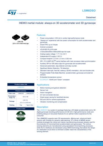
LSM6DSODatasheetiNEMO inertial module: always-on 3D accelerometer and 3D gyroscopeFeaturesLGA-14L(2.5 x 3.0 x 0.83 mm) typ. SPI / I²C & MIPI I3CSM serial interface with main processor data synchronizationAuxiliary SPI for OIS data output for gyroscope and accelerometerAdvanced pedometer, step detector and step counterSignificant Motion Detection, Tilt detectionStandard interrupts: free-fall, wakeup, 6D/4D orientation, click and double-clickProgrammable Finite State Machine: accelerometer, gyroscope and externalsensorsEmbedded temperature sensor ECOPACK , RoHS and “Green” compliant Product status linkLSM6DSOProduct summaryOrder codeLSM6DSOTemperaturerange [ C]PackagePackingLSM6DSOTR-40 to 85LGA-14L(2.5 x 3 x 0.83 mm)TrayProduct labelPower consumption: 0.55 mA in combo high-performance mode“Always-on" experience with low power consumption for both accelerometer andgyroscopeSmart FIFO up to 9 kbyteAndroid compliant 2/ 4/ 8/ 16 g full scale 125/ 250/ 500/ 1000/ 2000 dps full scaleAnalog supply voltage: 1.71 V to 3.6 VIndependent IO supply (1.62 V)Compact footprint: 2.5 mm x 3 mm x 0.83 mmApplications Motion tracking and gesture detectionSensor hubIndoor navigationIoT and connected devicesSmart power saving for handheld devicesEIS and OIS for camera applicationsVibration monitoring and compensationTape & ReelDescriptionThe LSM6DSO is a system-in-package featuring a 3D digital accelerometer and a 3Ddigital gyroscope boosting performance at 0.55 mA in high-performance mode andenabling always-on low-power features for an optimal motion experience for theconsumer.The LSM6DSO supports main OS requirements, offering real, virtual and batchsensors with 9 kbytes for dynamic data batching. ST’s family of MEMS sensormodules leverages the robust and mature manufacturing processes already used forthe production of micromachined accelerometers and gyroscopes. The varioussensing elements are manufactured using specialized micromachining processes,while the IC interfaces are developed using CMOS technology that allows the designof a dedicated circuit which is trimmed to better match the characteristics of thesensing element.DS12140 - Rev 2 - January 2019For further information contact your local STMicroelectronics sales office.www.st.com
LSM6DSOThe LSM6DSO has a full-scale acceleration range of 2/ 4/ 8/ 16 g and an angularrate range of 125/ 250/ 500/ 1000/ 2000 dps.The LSM6DSO fully supports EIS and OIS applications as the module includes adedicated configurable signal processing path for OIS and auxiliary SPI, configurablefor both the gyroscope and accelerometer.High robustness to mechanical shock makes the LSM6DSO the preferred choice ofsystem designers for the creation and manufacturing of reliable products.TheLSM6DSO is available in a plastic land grid array (LGA) package.DS12140 - Rev 2page 2/172
LSM6DSOOverview1OverviewThe LSM6DSO is a system-in-package featuring a high-performance 3-axis digital accelerometer and 3-axisdigital gyroscope.The LSM6DSO delivers best-in-class motion sensing that can detect orientation and gestures in order toempower application developers and consumers with features and capabilities that are more sophisticated thansimply orienting their devices to portrait and landscape mode.The event-detection interrupts enable efficient and reliable motion tracking and contextual awareness,implementing hardware recognition of free-fall events, 6D orientation, click and double-click sensing, activity orinactivity, stationary/motion detection and wakeup events.The LSM6DSO supports main OS requirements, offering real, virtual and batch mode sensors. In addition, theLSM6DSO can efficiently run the sensor-related features specified in Android, saving power and enabling fasterreaction time. In particular, the LSM6DSO has been designed to implement hardware features such as significantmotion detection, stationary/motion detection, tilt, pedometer functions, timestamping and to support the dataacquisition of an external magnetometer.The LSM6DSO offers hardware flexibility to connect the pins with different mode connections to external sensorsto expand functionalities such as adding a sensor hub, auxiliary SPI, etc.Up to 9 kbytes of FIFO with compression and dynamic allocation of significant data (i.e. external sensors,timestamp, etc.) allows overall power saving of the system.Like the entire portfolio of MEMS sensor modules, the LSM6DSO leverages the robust and mature in-housemanufacturing processes already used for the production of micromachined accelerometers and gyroscopes. Thevarious sensing elements are manufactured using specialized micromachining processes, while the IC interfacesare developed using CMOS technology that allows the design of a dedicated circuit which is trimmed to bettermatch the characteristics of the sensing element.The LSM6DSO is available in a small plastic land grid array (LGA) package of 2.5 x 3.0 x 0.83 mm to addressultra-compact solutions.DS12140 - Rev 2page 3/172
LSM6DSOEmbedded low-power features2Embedded low-power featuresThe LSM6DSO has been designed to be fully compliant with Android, featuring the following on-chip functions: 9 kybtes data buffering, data can be compressed two or three times–100% efficiency with flexible configurations and partitioning–Possibility to store timestamp 2.1Event-detection interrupts (fully configurable)–Free-fall–Wakeup–6D orientation–Click and double-click sensing–Activity/Inactivity recognition–Stationary/Motion detectionSpecific IP blocks with negligible power consumption and high-performance–Pedometer functions: step detector and step counters–Tilt–Significant Motion Detection–Finite State Machine (FSM) for accelerometer, gyroscope, and external sensorsSensor hub–Up to 6 total sensors: 2 internal (accelerometer and gyroscope) and 4 external sensorsTilt detectionThe tilt function helps to detect activity change and has been implemented in hardware using only theaccelerometer to achieve targets of both ultra-low power consumption and robustness during the short duration ofdynamic accelerations.The tilt function is based on a trigger of an event each time the device's tilt changes and can be used withdifferent scenarios, for example:1.Triggers when phone is in a front pants pocket and the user goes from sitting to standing or standing tositting;2.Doesn’t trigger when phone is in a front pants pocket and the user is walking, running or going upstairs.2.2Significant Motion DetectionThe Significant Motion Detection (SMD) function generates an interrupt when a ‘significant motion’, that could bedue to a change in user location, is detected. In the LSM6DSO device this function has been implemented inhardware using only the accelerometer.SMD functionality can be used in location-based applications in order to receive a notification indicating when theuser is changing location.2.3Finite State MachineThe LSM6DSO can be configured to generate interrupt signals activated by user-defined motion patterns. To dothis, up to 16 embedded finite state machines can be programmed independently for motion detection such asglance gestures, absolute wrist tilt, shake and double-shake detection.Definition of Finite State MachineA state machine is a mathematical abstraction used to design logic connections. It is a behavioral modelcomposed of a finite number of states and transitions between states, similar to a flow chart in which one caninspect the way logic runs when certain conditions are met. The state machine begins with a start state, goes todifferent states through transitions dependent on the inputs, and can finally end in a specific state (called stopstate). The current state is determined by the past states of the system. Figure 1. Generic state machine shows ageneric state machine.DS12140 - Rev 2page 4/172
LSM6DSOFinite State MachineFigure 1. Generic state machineFinite State Machine in the LSM6DSOThe LSM6DSO works as a combo accelerometer-gyroscope sensor, generating acceleration and angular rateoutput data. It is also possible to connect an external sensor (magnetometer) by using the Sensor Hub feature(Mode 2). These data can be used as input of up to 16 programs in the embedded Finite State Machine(Figure 2. State machine in the LSM6DSO).All 16 finite state machines are independent: each one has its dedicated memory area and it is independentlyexecuted. An interrupt is generated when the end state is reached or when some specific command is performed.Figure 2. State machine in the LSM6DSODS12140 - Rev 2page 5/172
LSM6DSOPin description3Pin descriptionFigure 3. Pin connections3.1Pin connectionsThe LSM6DSO offers flexibility to connect the pins in order to have four different mode connections andfunctionalities. In detail:DS12140 - Rev 2 Mode 1: I²C / MIPI I3CSM slave interface or SPI (3- and 4-wire) serial interface is available; Mode 2: I²C / MIPI I3CSM slave interface or SPI (3- and 4-wire) serial interface and I²C interface master forexternal sensor connections are available; Mode 3: I²C / MIPI I3CSM slave interface or SPI (3- and 4-wire) serial interface is available for the applicationprocessor interface while an auxiliary SPI (3- and 4-wire) serial interface for external sensor connections isavailable for the gyroscope ONLY; Mode 4: I²C / MIPI I3CSM slave interface or SPI (3- and 4-wire) serial interface is available for the applicationprocessor interface while an auxiliary SPI (3- and 4-wire) serial interface for external sensor connections isavailable for the accelerometer and gyroscope.page 6/172
LSM6DSOPin connectionsFigure 4. LSM6DSO connection modesMode 1Mode 2Mode 3Mode 4HOSTHOSTHOSTHOSTI 2C /SMMIPI I3C /SPI (3/4-w)LSM6DSOI 2C /I 2C /MIPI I3CSM /SPI (3/4-w)I 2C /MIPI I3CSM /SPI (3/4-w)MIPI I3CSM /SPI (3/4-w)LSM6DSOMaster I2CLSM6DSOLSM6DSOAux SPI (3/4-w) For gyrodata onlyAux SPI (3/4-w) For XL andgyro amoduleIn the following table each mode is described for the pin connections and function.Table 1. Pin descriptionPin#DS12140 - Rev 2NameMode 1 functionMode 2 functionMode 3 / Mode 4 functionSPI 4-wire interface serial dataoutput (SDO)SPI 4-wire interface serial dataoutput (SDO)SPI 4-wire interface serial dataoutput (SDO)I²C least significant bit of thedevice address (SA0)I²C least significant bit of thedevice address (SA0)I²C least significant bit of the deviceaddress (SA0)1SDO/SA02SDxConnect to VDDIO or GNDI²C serial data master (MSDA)Auxiliary SPI 3/4-wire interface serialdata input (SDI) and SPI 3-wire serialdata output (SDO)3SCxConnect to VDDIO or GNDI²C serial clock master (MSCL)Auxiliary SPI 3/4-wire interface serialport clock (SPC Aux)4INT1Programmable interrupt in I²C and SPI5VDDIO(1)Power supply for I/O pins6GND0 V supply7GND0 V supply8VDD(1)Power supply9INT2Programmable interrupt 2(INT2) / Data enable (DEN)Programmable interrupt 2 (INT2)/Data enable (DEN)/I²C masterexternal synchronization signal(MDRDY)Programmable interrupt 2 (INT2)/Data enable (DEN)Auxiliary SPI 3/4-wire interfaceenable10OCS Aux Leave unconnected(2)Leave unconnected(2)11Connect to VDD IO or leaveSDO Auxunconnected(2)Connect to VDD IO or leaveunconnected(2)Auxiliary SPI 3-wire interface: leaveunconnected(2)Auxiliary SPI 4-wire interface: serialdata output (SDO Aux)page 7/172
LSM6DSOPin connectionsPin#1213NameCSSCLMode 1 functionMode 2 functionMode 3 / Mode 4 functionI²C/MIPI I3CSM/SPI modeselectionI²C/MIPI I3CSM/SPI modeselectionI²C/MIPI I3CSM/SPI mode selection(1: SPI idle mode / I²C/MIPII3CSM communication enabled;(1: SPI idle mode / I²C/MIPII3CSM communication enabled;0: SPI communication mode /I²C/MIPI I3CSM disabled)0: SPI communication mode / I²C/0: SPI communication mode / I²C/MIPI I3CSM disabled)SMMIPI I3C disabled)I²C/MIPI I3CSM serial clock(SCL)I²C/MIPI I3CSM serial clock (SCL)I²C/MIPI I3CSM serial clock (SCL)SPI serial port clock (SPC)SPI serial port clock (SPC)I²C/MIPI I3CSM serial data (SDA)I²C/MIPI I3CSM serial data (SDA)SPI serial data input (SDI)SPI serial data input (SDI)3-wire interface serial data output(SDO)3-wire interface serial dataSPI serial port clock (SPC)I²C/MIPI I3CSM serial data(SDA)14SDASPI serial data input (SDI)3-wire interface serial dataoutput (SDO)(1: SPI idle mode / I²C/MIPI I3CSMcommunication enabled;output (SDO)1. Recommended 100 nF filter capacitor.2. Leave pin electrically unconnected and soldered to PCB.DS12140 - Rev 2page 8/172
LSM6DSOModule specifications4Module specifications4.1Mechanical characteristics@ Vdd 1.8 V, T 25 C, unless otherwise noted.Table 2. Mechanical characteristicsSymbolParameterTest conditionsMin.Typ.(1)Max.Unit 2LA FS 4Linear acceleration measurement range 8g 16 125 250G FSAngular rate measurement range 500dps 1000 2000LA SoG SoG So%LA SoDrG SoDrLA TyOffG TyOffFS 2 g0.061FS 4 g0.122FS 8 g0.244FS 16 g0.488FS 125 dps4.375FS 250 dps8.75FS 500 dps17.50FS 1000 dps35FS 2000 dps70at component level 1%from -40 to 85 0.01%/ Cfrom -40 to 85 0.007%/ C 20mg 1dps 0.1mg/ C 0.010dps/ CRate noise density in high-performance mode(6)3.8mdps/ HzGyroscope RMS noise in normal/low-power mode(7)75mdpsLinear acceleration sensitivity(2)Angular ratesensitivity(2)Sensitivity tolerance(3)Linear acceleration sensitivity change vs.Angular rate sensitivity change vs.temperature(4)Linear acceleration zero-g level offsetAngular rate ure(4)LA OffDrLinear acceleration zero-g level change vs.G OffDrAngular rate typical zero-rate level change vs. temperature(4)RnRnRMSAnAcceleration noise density in high-performance mode(8)DS12140 - Rev 2FS 2 g70FS 4 g75FS 8 g80FS 16 g110mg/LSBmdps/LSBµg/ Hzpage 9/172
LSM6DSOMechanical characteristicsSymbolRMSParameterTest conditionsAcceleration RMS noise in normal/low-power mode(9) (10)Acceleration RMS noise in ultra-low-power mode(9)(10)Min.Typ.(1)FS 2 g1.8FS 4 g2.0FS 8 g2.4FS 16 g3.0FS 2 g5.5Max.Unitmg(RMS)1.6(11)12.52652104LA ODRLinear acceleration output data rate208416833166633326664Hz12.52652104G ODR208Angular rate output data rate416833166633326664Linear acceleration self-test outputVstTopchange(12)(13)(14)Angular rate self-test output change(15) (16)501700mgFS 250 dps2080dpsFS 2000 dps150700dps-40 85 COperating temperature range1. Typical specifications are not guaranteed.2. Sensitivity values after factory calibration test and trimming.3. Subject to change.4. Measurements are performed in a uniform temperature setup and they are based on characterization datain a limited number of samples. Not measured during final test for production.5. Values after factory calibration test and trimming.6. Gyroscope rate noise density in high-performance mode is independent of the ODR and FS setting.7. Gyroscope RMS noise in normal/low-power mode is independent of the ODR and FS setting.8. Accelerometer noise density in high-performance mode is independent of the ODR.9. Accelerometer RMS noise in normal/low-power/ultra-low-power mode is independent of the ODR.10. Noise RMS related to BW ODR/2.11. This ODR is available when the accelerometer is in low-power mode.12. The sign of the linear acceleration self-test output change is defined by the STx XL bits in a dedicatedregister for all axes.DS12140 - Rev 2page 10/172
LSM6DSOMechanical characteristics13. The linear acceleration self-test output change is defined with the device in stationary condition as theabsolute value of: OUTPUT[LSb] (self-test enabled) - OUTPUT[LSb] (self-test disabled). 1LSb 0.061 mgat 2 g full scale.14. Accelerometer self-test limits are full-scale independent.15. The sign of the angular rate self-test output change is defined by the STx G bits in a dedicated register forall axes.16. The angular rate self-test output change is defined with the device in stationary condition as the absolutevalue of: OUTPUT[LSb] (self-test enabled) - OUTPUT[LSb] (self-test disabled). 1LSb 70 mdps at 2000dps full scale.DS12140 - Rev 2page 11/172
LSM6DSOElectrical characteristics4.2Electrical characteristics@ Vdd 1.8 V, T 25 C, unless otherwise noted.Table 3. Electrical characteristicsMin.Typ.(1)Max.UnitSupply voltage1.711.83.6VPower supply for I/O1.623.6VSymbolVddVdd IOParameterTest conditionsGyroscope and accelerometer current consumption in high-performancemode0.55mALA IddHPAccelerometer current consumption in high-performance mode170µALA IddLPAccelerometer current consumption in low-power modeIddHPLA IddULP Accelerometer current consumption in ultra-low-power modeIddPDODR 52 Hz26ODR 1.6 Hz4.5ODR 52 Hz9.5ODR 1.6 Hz4.4µAµAGyroscope and accelerometer current consumption during power-down3µATonTurn-on time35msVIHDigital high-level input voltageVILDigital low-level input voltageVOHHigh-level output voltageIOH 4 mA(2)VOLLow-level output voltageIOL 4 mA(2)TopOperating temperature range0.7 *VDD IOV0.3 *VDD IOVVDD IO 0.2V-400.2V 85 C1. Typical specifications are not guaranteed.2. 4 mA is the maximum driving capability, i.e. the maximum DC current that can be sourced/sunk by the digitalpin in order to guarantee the correct digital output voltage levels VOH and VOL.4.3Temperature sensor characteristics@ Vdd 1.8 V, T 25 C unless otherwise noted.Table 4. Temperature sensor st conditionMin.Temperature refresh rateTemperatureMax.52offset(3)-15Temperature sensitivityTemperature stabilizationTyp.(1)Hz 15256time(4)T ADC resTemperature ADC resolutionTopOperating temperature range CLSB/ C50016-40Unitµsbit 85 C1. Typical specifications are not guaranteed.2. When the accelerometer is in low-power mode or ultra-low-power mode and the gyroscope part is turned off, the TODRvalue is equal to the accelerometer ODR.3. The output of the temperature sensor is 0 LSB (typ.) at 25 C.4. Time from power ON to valid data based on characterization data.DS12140 - Rev 2page 12/172
LSM6DSOCommunication interface characteristics4.4Communication interface characteristics4.4.1SPI - serial peripheral interfaceSubject to general operating conditions for Vdd and Top.Table 5. SPI slave timing values (in mode 3)ParameterSymbolValue(1)Mintc(SPC)SPI clock cyclefc(SPC)SPI clock frequencytsu(CS)CS setup time5th(CS)CS hold time20tsu(SI)SDI input setup time5th(SI)SDI input hold time15tv(SO)SDO valid output timeth(SO)SDO output hold timetdis(SO)SDO output disable timeMax100Unitns10MHzns505501. Values are guaranteed at 10 MHz clock frequency for SPI with both 4 and 3 wires, based on characterization results, nottested in productionFigure 5. SPI slave timing diagram (in mode 3)Note:DS12140 - Rev 2Measurement points are done at 0.2·Vdd IO and 0.8·Vdd IO for both input and output ports.page 13/172
LSM6DSOCommunication interface characteristics4.4.2I²C - inter-IC control interfaceSubject to general operating conditions for Vdd and Top.Table 6. I²C slave timing valuesSymbolI²C standard mode(1)Parameterf(SCL)I²C fast mode (1)MinMaxMinMax01000400SCL clock frequencytw(SCLL)SCL clock low time4.71.3tw(SCLH)SCL clock high time4.00.6tsu(SDA)SDA setup time250100th(SDA)SDA data hold time0th(ST)START condition hold time40.6tsu(SR)Repeated START condition setup time4.70.6tsu(SP)STOP condition setup time40.64.71.3tw(SP:SR)Bus free time between STOP and START condition3.45UnitkHzµsns00.9µsµs1. Data based on standard I²C protocol requirement, not tested in production.Figure 6. I²C slave timing A)STARTth(SDA)tsu(SP)STOPSCLth(ST)Note:DS12140 - Rev 2tw(SCLL)tw(SCLH)Measurement points are done at 0.2·Vdd IO and 0.8·Vdd IO for both ports.page 14/172
LSM6DSOAbsolute maximum ratings4.5Absolute maximum ratingsStresses above those listed as “Absolute maximum ratings” may cause permanent damage to the device. This isa stress rating only and functional operation of the device under these conditions is not implied. Exposure tomaximum rating conditions for extended periods may affect device reliability.Table 7. Absolute maximum ratingsSymbolMaximum valueUnitVddSupply voltage-0.3 to 4.8VTSTGStorage temperature range-40 to 125 C20,000g2kV-0.3 to Vdd IO 0.3VSgESDVinNote:RatingsAcceleration g for 0.2 msElectrostatic discharge protection (HBM)Input voltage on any control pin(including CS, SCL/SPC, SDA/SDI/SDO, SDO/SA0)Supply voltage on any pin should never exceed 4.8 V.This device is sensitive to mechanical shock, improper handling can cause permanent damage to the part.This device is sensitive to electrostatic discharge (ESD), improper handling can cause permanent damage to the part.DS12140 - Rev 2page 15/172
near acceleration sensitivity can be determined, for example, by applying 1 g acceleration to the device.Because the sensor can measure DC accelerations, this can be done easily by pointing the selected axis towardsthe ground, noting the output value, rotating the sensor 180 degrees (pointing towards the sky) and noting theoutput value again. By doing so, 1 g acceleration is applied to the sensor. Subtracting the larger output valuefrom the smaller one, and dividing the result by 2, leads to the actual sensitivity of the sensor. This value changesvery little over temperature and over time. The sensitivity tolerance describes the range of sensitivities of a largenumber of sensors (see Table 2).An angular rate gyroscope is a device that produces a positive-going digital output for counterclockwise rotationaround the axis considered. Sensitivity describes the gain of the sensor and can be determined by applying adefined angular velocity to it. This value changes very little over temperature and time (see Table 2).4.6.2Zero-g and zero-rate levelLinear acceleration zero-g level offset (TyOff) describes the deviation of an actual output signal from the idealoutput signal if no acceleration is present. A sensor in a steady state on a horizontal surface will measure 0 g onboth the X-axis and Y-axis, whereas the Z-axis will measure 1 g. Ideally, the output is in the middle of the dynamicrange of the sensor (content of OUT registers 00h, data expressed as 2’s complement number). A deviation fromthe ideal value in this case is called zero-g offset.Offset is to some extent a result of stress to MEMS sensor and therefore the offset can slightly change aftermounting the sensor onto a printed circuit board or exposing it to extensive mechanical stress. Offset changeslittle over temperature, see “Linear acceleration zero-g level change vs. temperature” in Table 2. Mechanicalcharacteristics. The zero-g level tolerance (TyOff) describes the standard deviation of the range of zero-g levels ofa group of sensors.Zero-rate level describes the actual output signal if there is no angular rate present. The zero-rate level of preciseMEMS sensors is, to some extent, a result of stress to the sensor and therefore the zero-rate level can slightlychange after mounting the sensor onto a printed circuit board or after exposing it to extensive mechanical stress.This value changes very little over temperature and time (see Table 2. Mechanical characteristics).DS12140 - Rev 2page 16/172
LSM6DSODigital interfaces5Digital interfaces5.1I²C/SPI interfaceThe registers embedded inside the LSM6DSO may be accessed through both the I²C and SPI serial interfaces.The latter may be SW configured to operate either in 3-wire or 4-wire interface mode. The device is compatiblewith SPI modes 0 and 3.The serial interfaces are mapped onto the same pins. To select/exploit the I²C interface, the CS line must be tiedhigh (i.e connected to Vdd IO).Table 8. Serial interface pin descriptionPin namePin descriptionSPI enableCSI²C/SPI mode selection (1: SPI idle mode / I²C communication enabled;0: SPI communication mode / I²C disabled)I²C Serial Clock (SCL)SCL/SPCSPI Serial Port Clock (SPC)I²C Serial Data (SDA)SDA/SDI/SDOSPI Serial Data Input (SDI)3-wire Interface Serial Data Output (SDO)SDO/SA05.1.1SPI Serial Data Output (SDO)I²C less significant bit of the device addressI²C serial interfaceThe LSM6DSO I²C is a bus slave. The I²C is employed to write the data to the registers, whose content can alsobe read back.The relevant I²C terminology is provided in the table below.Table 9. I²C terminologyTermTransmitterReceiverDescriptionThe device which sends data to the busThe device which receives data from the busMasterThe device which initiates a transfer, generates clock signals and terminates a transferSlaveThe device addressed by the masterThere are two signals associated with the I²C bus: the serial clock line (SCL) and the Serial DAta line (SDA). Thelatter is a bidirectional line used for sending and receiving the data to/from the interface. Both the lines must beconnected to Vdd IO through external pull-up resistors. When the bus is free, both the lines are high.The I²C interface is implemented with fast mode (400 kHz) I²C standards as well as with the standard mode.In order to disable the I²C block, (I2C disable) 1 must be written in CTRL4 C (13h).DS12140 - Rev 2page 17/172
LSM6DSOI²C/SPI interfaceI²C operationThe transaction on the bus is started through a START (ST) signal. A START condition is defined as a HIGH toLOW transition on the data line while the SCL line is held HIGH. After this has been transmitted by the master, thebus is considered busy. The next byte of data transmitted after the start condition contains the address of theslave in the first 7 bits and the eighth bit tells whether the master is receiving data from the slave or transmittingdata to the slave. When an address is sent, each device in the system compares the first seven bits after a startcondition with its address. If they match, the device considers itself addressed by the master.The Slave ADdress (SAD) associated to the LSM6DSO is 110101xb. The SDO/SA0 pin can be used to modify theless significant bit of the device address. If the SDO/SA0 pin is connected to the supply voltage, LSb is ‘1’(address 1101011b); else if the SDO/SA0 pin is connected to ground, the LSb value is ‘0’ (address 1101010b).This solution permits to connect and address two different inertial modules to the same I²C bus.Data transfer with acknowledge is mandatory. The transmitter must release the SDA line during the acknowledgepulse. The receiver must then pull the data line LOW so that it remains stable low during the HIGH period of theacknowledge clock pulse. A receiver which has been addressed is obliged to generate an acknowledge after eachbyte of data received.The I²C embedded inside the LSM6DSO behaves like a slave device and the following protocol must be adheredto. After the start condition (ST) a slave address is sent, once a slave acknowledge (SAK) has been returned, an8-bit sub-address (SUB) is transmitted. The increment of the address is configured by the CTRL3 C (12h)(IF INC).The slave address is completed with a Read/Write bit. If the bit is ‘1’ (Read), a repeated START (SR) conditionmust be issued after the two sub-address bytes; if the bit is ‘0’ (Write) the master will transmit to the slave withdirection unchanged. Table 10 explains how the SAD Read/Write bit pattern is composed, listing all the possibleconfigurations.Table 10. SAD Read/Write patternsCommandSAD[6:1]SAD[0] SA0R/WSAD R/WRead1101010111010101 (D5h)Write1101010011010100 (D4h)Read1101011111010111 (D7h)Write1101011011010110 (D6h)Table 11. Transfer when master is writing one byte to slaveMasterSTSAD WSUBSlaveSAKDATASPSAKSAKTable 12. Transfer when master is writing multiple bytes to slaveMasterSTSAD WSUBSlaveSAKDATASAKDATASAKSPSAKTable 13. Transfer when master is receiving (reading) one byte of data from slaveMasterSTSAD WSlaveSUBSAKSRSAD RSAKNMAKSAKSPDATATable 14. Transfer when master is receiving (reading) multiple bytes of data from slaveMasterSTDS12140 - Rev 2SAD WSUBSRSAD RMAKMAKNMAKSPpage 18/172
LSM6DSOI²C/SPI interfaceSlaveSAKSAKSAKDATADATADATAData are transmitted in byte format (DATA). Each data transfer contains 8 bits. The number of bytes transferredper transfer is unlimited. Data is transferred with the Most Significant bit (MSb) first. If a receiver can’t receiveanother complete byte of data until it has performed some other function, it can hold the clock line, SCL LOW toforce the transmitter into a wait state. Data transfer only continues when the receiver is ready for another byte andreleases the data line. If a slave receiver doesn’t acknowledge the slave address (i.e. it is not able to receivebecause it is performing some real-time function) the data line must be left HIGH by the slave. The master canthen abort the transfer. A LOW to HIGH transition on the SDA line while the SCL line is HIGH is defined as aSTOP condition. Each data transfer must be terminated by the generation of a STOP (SP) condition.In the presented communication format MAK is Master acknowledge and NMAK is No Master Acknowledge.DS12140 - Rev 2page 19/172
LSM6DSOI²C/SPI interface5.1.2SPI bus interfaceThe LSM6DSO SPI is a bus slave. The SPI allows writing and reading the registers of the device.The serial interface communicates to the application using 4 wires: CS, SPC, SDI and SDO.Figure 7. Read and write protocol (in mode 3)CSSPCSDIRWDI7 DI6 DI5 DI4 DI3 DI2 DI1 DI0AD6 AD5 AD4 AD3 AD2 AD1 AD0SDODO7 DO6 DO5 DO4 DO3 DO2 DO1 DO0CS is the serial port enable and it is controlled by the SPI master. It goes low at the start of the transmission andgoes back high at the end. SPC is the serial port clock and it is controlled by the SPI master. It is stopped highwhen CS is high (no transmission). SDI and SDO are, respectively, the serial port data input and output. Thoselines are driven at the falling edge of SPC and should be captured at the rising edge of SPC.Both the read register and write register commands are completed in 16 clock pulses or in multiples of 8 in caseof multiple read/write bytes. Bit duration is the time between two falling e
The LSM6DSO has been designed to be fully compliant with Android, featuring the following on-chip functions: 9 kybtes data buffering, data can be compressed two or three times - 100% efficiency with flexible configurations and partitioning - Possibility to store timestamp Event-detection interrupts (fully configurable) - Free-fall