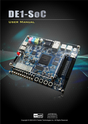
Transcription
Tutorial for Altera DE1 and Quartus IIQin-Zhong YeDecember, 2013This tutorial teaches you the basic steps to use Quartus II version 13.0 to program Altera’sFPGA, Cyclone II EP2C20 on the Development & Education Board DE1. One can also use itas a simplified user manual.Some screen prints are taken from Quartus II version 9 and therefore may be slightly differentfrom that of Quartus II version 13.0.Contents1.Create a new project . 22.Copy VHDL files and the assignment file for DE1 . 93.Create a new schematic file . 94.Open an existing VHDL file and add it to a project . 135.Create a symbol for a VHDL file . 166.Importing symbols to the schematic file . 187.Importing assignments . 218.Importing input and output symbols . 239.Connect symbols in a schematic . 2610. Connect individual signals to a bus . 2711. Specify the unused pins setting . 3012. Compilation. 3313. Programming FPGA Chip . 3414. Viewing implementation logic . 3615. Checking the problem with pin assignment . 3716. How to update a symbol after making changes to signal names . 3917. What to do after add/remove input/output signals in a VHDL file . 4118. How to create a VHDL file for the schematic file . 4219. How to copy a project . 4320. How to change top-level entity . 4421. How to change revision name . 4522. How to use In-System Sources and Probes Editor . 4823. How to install USB driver. 54December 3, 20131
1. Create a new project(Notice that you should create a working directory in the local disk (e.g., D:\) of the PCbefore creating a new project.)Click ”Create a New Project”.Click ”Next”.December 3, 20132
Change the working directory name to your own working directory name. A workingdirectory in the local drive (e.g., D:\) of the PC is preferred.December 3, 20133
Fill in the name of your project. Click “Next”.Click ”Ja”.December 3, 20134
If there is no design file (e.g. schematic or VHDL files) to add, click “Next”.December 3, 20135
If the selected device is EP2C20F484C7, click “Next”.December 3, 20136
Click “Next”.December 3, 20137
Click “Finish”.December 3, 20138
2. Copy VHDL files and the assignment file for DE1Use Windows Explorer to copy all files in the directory“S:\TN\E\094 Digitalteknik och konstruktion\VHDL and assignment files” to your projectdirectory.3. Create a new schematic fileSelect “File New ”December 3, 20139
Select “BlockDiagram/Schematic File” and click “OK”.December 3, 201310
Select “File Save as ” to change the file name to a new name. This file name of theschematic will be used as the “top-level design entity” name of your whole design. Youshould choose the same name as the name of “top-level design entity”. However, pleasenotice that the file name for the schematic cannot be the same as any entity name in theVHDL codes.December 3, 201311
Click “Spara”. Notice that the file name “Counter example” should be the same as the “toplevel design entity” name.December 3, 201312
4. Open an existing VHDL file and add it to a projectSelect “File Open ”. Find the VHDL file and click “Öppna”.Notice that you should have already copied all files in the directory“S:\TN\E\094 Digitalteknik och konstruktion\VHDL and assignment files” to your projectdirectory.December 3, 201313
Select “Project Add/Remove Files in Project ” in the main toolbar.Click “Add All”. (Notice that you should have already copied all files in the directory“S:\TN\E\094 Digitalteknik och konstruktion\VHDL and assignment files” to your projectDecember 3, 201314
directory.) (Alternatively, you can also click “ ” and navigate to your project directory andfind the VHDL files.)The list shows that two VHDL files are added to your project. Click “OK”.December 3, 201315
5. Create a symbol for a VHDL fileClick the file symbol at the bottom of the Project Navigator. Double-click “Counter27bit.vhd”to open it.(Alternatively, if you don’t want to open the VHDL file, you can right-click on the file name“Counter27bit.vhd” in the file list and choose “Create Symbol files for Current file” in thepop-up menu.)December 3, 201316
Select “Processing Analyze Current File”.Click “OK”.Click “File Create/Update Create Symbol Files for Current File”.Click “OK”.Perform the same operations (i.e., open file, analyze file, create symbol files) as above for theVHDL file “Seven seg.vhd”.December 3, 201317
6. Importing symbols to the schematic fileClick “Counter example.bdf” to view the schematic file.Double-click on the blank space of the Graphic Editor window or click on the AND-gate iconin the toolbar.Click the “ ” sign to expand “Project” in the Libraries box.December 3, 201318
Select “Counter27bit”.Click “OK”.December 3, 201319
The symbol for “Counter27bit” will appear in the Graphic Editor window. Move the symbolto a proper location and click the left mouse button. If the symbol continues to follow themouse movement, click on the “Esc” button on your keyboard or click the right button of themouse and select “Cancel”.Perform the same operations as above for the symbol “bcd7seg”. Notice that the symbol name“bcd7seg” is the same as the entity name in the VHDL file “seven seg.vhd”.December 3, 201320
7. Importing assignmentsYou should use the assignment file “DE1 pin assignments.csv” for your project. In thisassignment file, input and output signal names are assigned to the pins of FPGA. These pinsof FPGA are connected to various components on the printed circuit board. Click“Assignments Import Assignments ” in the main toolbar.Click “ ” to find the assignment file.December 3, 201321
Click “Öppna”.Click “OK”.December 3, 201322
Click “Assignments Pin Planner” in the main toolbar.The content of the assignment file is shown in the lower part of the window. If you want toconnect the output signals of the 7-segment decoder to the input signals of a 7-segmentdisplay on DE1, you should use the pre-defined output signal names in the Node Namecolumn of the assignment editor. For example, HEX0[0], HEX0[1], HEX0[6] are the 7output signals of the right-most 7-segment display on DE1. The input pins of the display areconnected to 7 output pins of the FPGA chip. For each pre-defined signal name, you can findthe corresponding pin of the FPGA chip in the column “Location”. The 50 MHz oscillator onDE1 has a pre-defined input signal name CLOCK 50 and it is connected to the pin “PIN L1”of the FPGA chip.8. Importing input and output symbolsDouble-click on the blank space of the Graphic Editor window or click on the AND-gate iconin the toolbar.December 3, 201323
Click the “ ” sign to expand “c:/altera/13.0/quartus/libraries” in the Libraries box. You canexpand the hierarchy as show in the follow window to find input and output symbols.(Notice that you can also find the instructions for importing input and output symbols as inthe tutorial “tut quartus intro schem.pdf”.)Click “OK”.December 3, 201324
The symbol will appear in the schematic. You can move the symbol by using the mouse.When the symbol is at the correct position, left-click to place the symbol. If the “repeat insertmode” is chosen, you can place several symbols. You can stop the repeated symbol placementby clicking “Esc” key on the keyboard.Double-click on the symbol in the schematic, the following window is shown.You should use these pre-defined names (e.g., HEX0[0], CLOCK 50, etc.) as the pin namesfor input and output symbols. Since the output of the 7-segment decoder is a bus. The outputsymbol should also be a bus. Use the notation HEX0[0.6] as the pin name. Click “OK”.December 3, 201325
9. Connect symbols in a schematicClick “Orthogonal Node Tool” (for a single signal) in the toolbar. Use the tool to connect theinput CLOCK 50 to the Clk input of Counter27bit.Click “Orthogonal Bus Tool” (for a bus) in the toolbar. Use the tool to connect the output ofthe decoder to the output symbol.December 3, 201326
10. Connect individual signals to a busConnect the counter and the 7-segment decoder as shown in the following window.Assign a name to a busClick the selection tool (Arrow) in the toolbar. Select the bus connected to the input of the 7segment decoder. Right-click on the bus and select “Properties”. The following window willappear.December 3, 201327
Fill in a bus name (any name you like). Click “OK”.Assign a name to a node (signal) lineClick the selection tool (Arrow) in the toolbar. Select the node (signal) line connected to theoutput of the counter. Right-click on the line and select “Properties”. The following windowwill appear.Fill in a node (signal) line name which is connected to a single bit of the connected bus. Forthe output signal “clkbit26”, the node line name is b[3]. Click “OK”.Assign node line names to the other 3 lines. The result is shown in the following window.Save the file.December 3, 201328
December 3, 201329
11. Specify the unused pins settingClick “Assignments Device ” in the main toolbar, the “Device” window is shown.Click “Device and Pin Option ” icon.December 3, 201330
Select “Unused Pins” in “Category”December 3, 201331
In the pull-down menu, select “As input tri-stated”. Click “OK”.Click “OK” in the “Device” window.December 3, 201332
12. CompilationClick “Processing Start Compilation”.If the compilation is successful, the following window is displayed.The large number of warnings is due to the unused node names in the assignment file.Click “Assignments Pins” in the main menu. Observe that the used pins are moved to thetop of the list as shown in the following window.December 3, 201333
13. Programming FPGA ChipCheck whether the AC/DC adapter and the USB cable are connected. Turn on the power ofDE1 by pushing the red button on DE1.Click “Tools Programmer” in the main toolbar.Make sure the Mode is “JTAG”. Click “Start”. If “Start” is not clickable, as shown in thefollowing window, click “Hardware Setup ”.December 3, 201334
Click “Hardware Setup ” at the upper-left corner of the window.In the pull-down menu for “Currently selected hardware”, select “USB-Blaster[USB-0]”.Click “Close”. Now “Start” should be clickable. (Notice that USB driver for DE1 shouldhave been installed. If it is not installed, follow the instructions in chapter 22, How to installUSB driver.)December 3, 201335
14. Viewing implementation logicClick “Tools Netlist Viewers RTL Viewer”.Double click the symbols to expand “counter27bit” and “bcd7seg” to view details.December 3, 201336
Chapters 15 – 23 are not tutorial steps and may be used as asimple user manual.15. Checking the problem with pin assignmentNote that this chapter is not a tutorial step. When you are looking for the reasons why youcircuit does not work, you may need to read this chapter and check whether you have aproblem with pin assignment.One problem with the pin assignment in Quartus II version 13.0 is the setting for “BlockDesign Naming”. After compilation of your schematic and VHDL codes with the schematicas the top-level design entity, you should find the names of the input and output signals whichyou have used in the schematic at the top of the node name list in Pin Planner. If you find thatthere are other signal names which are added into the node name list, it is an indication thatthe setting for “Block Design Naming” is causing a problem for the compilation. Thesynthesized circuit may not work properly. The in-system sources and probes may also beaffected by this problem.You can correct the setting for “Block Design Naming” as follows.Click on “Assignment Settings ” in the main toolbar, the following window is shown.December 3, 201337
Click on “Analysis & Synthesis Settings” and the click on “More settings ” button. Thefollowing window is shown.Double-click on “Auto” of the setting ”Block Design Naming”. The pull-down menu willshow 3 alternatives. Select “Quartus II” and click “OK” to close the window.Compile your project again and check whether the synthesized circuit works. Note that theadded names in the node name list might still be there in “Pin Planner”. But they are notcausing the problem. (If you notice any problems or errors with this part of text, please let meknow.)December 3, 201338
16. How to update a symbol after making changes tosignal namesIf you change the names of any input/output signals in a VHDL file, you should do thefollowing steps:Click “Processing Analyze Current File” to check the modified VHDL code.View the schematic in Graphic Editor. Right-click on the symbol.Select “Edit Selected Symbol” from the pull-down menu.December 3, 201339
Change the names of the signalsDouble-click on the name of the signal.Change the signal name and click “OK”. Save the file.December 3, 201340
Update symbolsRight-click in the blank space of the Graphic Editor and click “Update Symbol or Block ”.Click “OK”.17. What to do after add/remove input/output signals ina VHDL fileIf you add/remove input/output signals in a VHDL file, you should create the symbol again byclicking “File Create/Update Create Symbol Files for Current File” and adding the newsymbol to the schematic file.December 3, 201341
18. How to create a VHDL file for the schematic fileClick “File Create/Update Create HDL Design File for Current File”.Click “OK”.Notice that the created file is not added in the project since this file is not needed forcompilation of your design. The VHDL file is useful if you want to move your design toanother design tool or software.If you want to view it, you can open this file by clicking “File Open ”.Select the VHDL file “counter example” and click “Öppna”.The code is an example of the structural style VHDL code. There are 2 components,“bcd7seg” and “counter27bit”, in the code.December 3, 201342
19. How to copy a projectIt is possible to copy an existing project and give the copied project a new project name. Thecopied project can be further improved by adding new components and VHDL codes.Click “Project- Project copy ”. When the “Copy Project” window pops up, change the“Destination directory” and the “New project name” and click “OK”.If the “Destination directory” does not exist, the following window pops up. Click “Yes”.December 3, 201343
20. How to change top-level entitySometimes, you need to change top-level entity before compiling the design. For example,after copying a project, if you click “File- Save As ” to change the file name of theschematic to a new name, you need to change the top-level entity.Click “Assignments- Settings ”. Click “General”.Type a newentity nameSelect an entityfrom an entitylistSelect an entity from the pull-down list for “Top-level entity”. Some entity names in the listare the entity names in the VHDL codes. (Notice that entity names may be different from theVHDL file names!) There is also an entity name for the schematic in the list. The entity nameis the same as the file name of the schematic. If the new entity name for the schematic is notin the list, you should change the top-level entity by typing the new entity name.If you only want to compile a VHDL code, you can select the entity name of the entity in theVHDL code.If you want to compile the whole design, you should select the entity name for the schematic.December 3, 201344
21. How to change revision nameA revision name is used to set the output file names after compilation.Revision nameFor example, the revision name is used as the name of the file to be downloaded into FPGA.December 3, 201345
If you want to change the revision name, click “Project- Revisions ”.Click the button “Create ”. In other versions of Quartus II, the window may also look likethe following one. Click new revision to create a new revirsion.December 3, 201346
Fill in a new revision name and click “OK”.Click “OK”.Notice that, in the above window, if you want to delete the old revision, you can click therevision name in the list and click the button “Delete”. All the output files of the revision willbe deleted.December 3, 201347
22. How to use In-System Sources and Probes EditorThe In-System Sources and Probes Editor in the Quartus II software allows you to easilycontrol any internal signal and provides you with a completely dynamic debuggingenvironment. You can get more information on the In-System Sources and Probes Editor fromthe Quartus II Handbook, Chapter 16 (Volume 3: Verification, Section IV: System DebuggingTools).The In-System Sources and Probes Editor consists of the ALTSOURCE PROBEmegafunction and an interface to control the ALTSOURCE PROBE megafunction instancesduring run time. Each ALTSOURCE PROBE megafunction instance provides you withsource output ports and probe input ports, where source ports drive selected signals and probeports sample selected signals. When you compile your design, the ALTSOURCE PROBEmegafunction sets up a register chain to either drive or sample the selected nodes in your logicdesign. During run time, the In-System Sources and Probes Editor uses a JTAG connection toshift data to and from the ALTSOURCE PROBE megafunction instances.Configuring the ALTSOURCE PROBE MegafunctionTo use the In-System Sources and Probes Editor in your design, you must first instantiate theALTSOURCE PROBE megafunction variation file. You can configure theALTSOURCE PROBE megafunction with the MegaWizard Plug-In Manager.Each source or probe port can be up to 256 bits. You can have up to 128 instances of theALTSOURCE PROBE megafunction in your design.To configure the ALTSOURCE PROBE megafunction, performing the following steps:1. On the Tools menu, click MegaWizard Plug-In Manager.2. Select Create a new custom megafunction variation.December 3, 201348
3. Click Next.4. On page 2a of the MegaWizard Plug-In Manager, make the following selections:a. In the Installed Plug-Ins list, expand the JTAG-accessible Extensions folder and select InSystem Sources and Probes. (You can also verify that the currently selected device familymatches the device you are targeting.)b. Select an output file type and enter the name (for example, source probe1) of theALTSOURCE PROBEmegafunction. You can choose AHDL (.tdf), VHDL (.vhd), or Verilog HDL (.v) as theoutput file type.5. Click Next.December 3, 201349
6. On page 3 of the MegaWizard Plug-In Manager, make the following selections:a. Under Do you want to specify an Instance Index?, turn on Yes. This index determines theposition of the instance in the list of instances of the In-System Sources and probes Editor.b. Specify the ‘Instance ID’ of this instance.c. Specify the width of the probe port. The width can be from 0 bit to 256 bits.d. Specify the width of the source port. The width can be from 0 bit to 256 bits.7. On page 3 of the MegaWizard Plug-In Manager, you can click Advanced Options andspecify other options, including the following: What is the initial value of the source port, in hexadecimal? — Allows you to specify theinitial value driven on the source port at run time. Write data to the source port synchronously to the source clock — Allows you tosynchronize your source port write transactions with the clock domain of your choice. Create an enable signal for the registered source port—When turned on, creates a clockenable input for the synchronization registers. You can turn on this option only when theWrite data to the source port synchronously to the source clock option is turned on.8. Click Next.December 3, 201350
9. Click Next.10. Select (tick) soure probe1.bsf to create a Quartus II symbol file. The symbol can beimported to the schematic of your design. (Sinec the file “source probe1.vhd” is alwayscreated, you can also create the symbol for the VHDL file. See Chapter 5, Create a symbol fora VHDL file,”, of this document.)11. Click Finish.December 3, 201351
12. Click Yes.Import the created symbol to the schematic of your projectFollow the instructions in Chapter 6, Importing symbols to the schematic file, of thisdocument.Compile the projectClick “Processing Start Compilation”. See Chapter 12, Compilation, of this document.Program FPGA ChipClick “Tools Programmer”. See Chapter 13, Programming FPGA Chip, of this document.Running the In-System Sources and Probes Editor1. Open the In-System Sources and Probes Editor. Click “Tools In-System Sources andProbes Editor”.If you have not programed FPGA chip, you should do Steps 2 - 5 to program FPGA chip.Otherwise, you can skip Steps 2– 5.2. In the JTAG Chain Configuration pane, point to Hardware, and then select the hardwarecommunications device. You may be prompted to configure your hardware; in this case, clickSetup.3. From the Device list, select the FPGA device to which you want to download the design(the device may be automatically detected). You may need to click ScanChain to detect your target device.4. In the JTAG Chain Configuration pane, click to browse for the SRAM Object File(.sof) that includes the In-System Sources and Probes instance or instances. (The.sof may be automatically detected).5. Click Program Device to program the target device.Instance ManagerThe Instance Manager pane provides a list of all ALTSOURCE PROBE instances in thedesign and allows you to configure how data is acquired from or written to those instances.The following buttons and sub-panes are provided in the Instance Manager pane: Read Probe Data—Samples the probe data in the selected instance and displays the probedata in the In-System Sources and Probes Editor pane. Continuously Read Probe Data—Continuously samples the probe data of the selectedinstance and displays the probe data in the In-System Sources andProbes Editor pane; you can modify the sample rate via the Probe read interval setting.December 3, 201352
Stop Continuously Reading Probe Data—Cancels continuous sampling of the probe of theselected instance. Write Source Data—Writes data to all source nodes of the selected instance. Probe Read Interval—Displays the sample interval of all the In-System Sources and Probeinstances in your design; you can modify the sample interval by clicking Manual. Event Log—Controls the event log in the In-System Sources and Probes Editor pane. Write Source Data—Allows you to manually or continuously write data to the system.The status of each instance is also displayed beside each entry in the Instance Manager pane.The status indicates if the instance is Not running Offloading data, Updating data, or if anUnexpected JTAG communication error occurs. This status indicator provides informationabout the sources and probes instances in your design.In-System Sources and Probes Editor PaneThe In-System Sources and Probes Editor pane allows you to view data from all sources andprobes in your design. The data is organized according to the index number of the instance.The editor provides an easy way to manage your signals, and allows you to rename signals orgroup them into buses. All data collected from in-system source and probe nodes is recordedin the event log and you can view the data as a timing diagram.Reading Probe DataYou can read data by selecting the ALTSOURCE PROBE instance in the Instance Managerpane and clicking Read Probe Data. This action produces a single sample of the probe dataand updates the data column of the selected index in the In-SystemSources and Probes Editor pane. You can save the data to an event log by turning on the Savedata to event log option in the Instance Manager pane.If you want to sample data from your probe instance continuously, in the Instance Managerpane, click the instance you want to read, and then click Continuously read probe data. Whilereading, the status of the active instance shows Unloading. You can read continuously frommultiple instances.You can access read data with the shortcut menus in the Instance Manager pane.To adjust the probe read interval, in the Instance Manager pane, turn on the Manual option inthe Probe read interval sub-pane, and specify the sample rate in the text field next to theManual option. The maximum sample rate depends on your computer setup. The actualsample rate is shown in the Current interval box. You can adjust the event log window buffersize in the Maximum Size box.Writing DataTo modify the source data you want to write into the ALTSOURCE PROBE instance, clickthe name field of the signal you want to change. For buses of signals, you can double-click thedata field and type the value you want to drive out to the ALTSOURCE PROBE instance.The In-System Sources and Probes Editor stores the modified source data values in atemporary buffer. Modified values that are not written out to the ALTSOURCE PROBEinstances appear in red. To update the ALTSOURCE PROBE instance, highlight the instancein the Instance Manager pane and click Write source data. The Write source data function isalso available via the shortcut menus in the Instance Manager pane.The In-System Sources and Probes Editor provides the option to continuously update eachALTSOURCE PROBE instance. Continuous updating allows any modifications you make tothe source data buffer to also write immediately to the ALTSOURCE PROBE instances. Tocontinuously update the ALTSOURCE PROBE instances, change the Write source data fieldfrom Manually to Continuously.December 3, 201353
Organizing DataThe In-System Sources and Probes Editor pane allows you to group signals into buses, andalso allows you to modify the display options of the data buffer.To create a group of signals, select the node names you want to group, right-click and selectGroup. You can modify the display format in the Bus Display Format and theBus Bit order shortcut menus.The In-System Sources and Probes Editor pane allows you to rename any signal. To rename asignal, double-click the name of the signal and type the new name.The event log contains a record of the most recent samples. The buffer size is adjustable up to128k samples. The time stamp for each sample is logged and is displayed above the event logof the active instance as you move your pointer over the data samples.You can save the changes that you make and the recorded data to a Sources and Probes File(.spf). To save changes, on the File menu, click Save. The file contains all the modificationsyou made to the signal groups, as well as the current data event log.23. How to install USB driverUSB blaster is the USB device on Altera’s FPGA board, DE1. When DE1 is connected to aPC through a USB cable, the USB driver for USB Blaster should be installed. The USB drivercan be found in the folder “\altera\91sp2\quartus\drivers\usb-blaster”, if Quartus II version 9.1is installed on the PC.When DE1 is connected to a PC with Windows XP, a pop-up window “Found NewHardware Wizard” will be shown to guide the installation of the driver. See the details in themanual “Getting started with Altera DE1.pdf”.When DE1 is connected to a PC with Windows Vista, a pop-up window will be shown toguide the installation of the driver. Similar steps as for Windows XP should be done.When DE1 is connected to a PC with Windows 7, no pop-up window will be shown. Oneshould follow the following steps in “Manual for installation of Quartus II and USB driver forWindows 7” in “Manual install Quartus USBdriver Windows 7.pdf” to install the USBdriver.December 3, 201354
This tutorial teaches you the basic steps to use Quartus II version 13.0 to program Altera's FPGA, Cyclone II EP2C20 on the Development & Education Board DE1. One can also use it as a simplified user manual. Some screen prints are taken from Quartus II version 9 and therefore may be slightly different from that of Quartus II version 13.0 .