Transcription
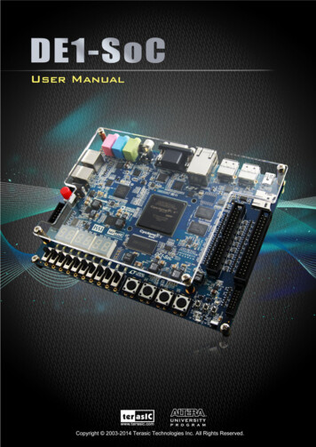
i3DE1-SoC User Manual1www.terasic.comJanuary 28, 2019
CONTENTSChapter 1DE1-SoC Development Kit . 41.1 Package Contents . 41.2 DE1-SoC System CD . 51.3 Getting Help . 5Chapter 2Introduction of the DE1-SoC Board . 62.1 Layout and Components. 62.2 Block Diagram of the DE1-SoC Board . 8Chapter 3Using the DE1-SoC Board . 123.1 Settings of FPGA Configuration Mode . 123.2 Configuration of Cyclone V SoC FPGA on DE1-SoC . 133.3 Board Status Elements. 193.4 Board Reset Elements . 203.5 Clock Circuitry . 213.6 Peripherals Connected to the FPGA. 233.6.1User Push-buttons, Switches and LEDs . 233.6.27-segment Displays . 263.6.32x20 GPIO Expansion Headers . 283.6.424-bit Audio CODEC . 303.6.5I2C Multiplexer . 313.6.6VGA . 323.6.7TV Decoder . 353.6.8IR Receiver . 373.6.9IR Emitter LED . 37DE1-SoC User Manual1www.terasic.comJanuary 28, 2019
3.6.10SDRAM Memory . 383.6.11PS/2 Serial Port. 403.6.12A/D Converter and 2x5 Header . 423.7 Peripherals Connected to Hard Processor System (HPS). 433.7.1User Push-buttons and LEDs . 433.7.2Gigabit Ethernet. 443.7.3UART . 453.7.4DDR3 Memory . 463.7.5Micro SD Card Socket. 483.7.62-port USB Host . 493.7.7G-sensor. 503.7.8LTC Connector . 51Chapter 4DE1-SoC System Builder . 534.1 Introduction . 534.2 Design Flow . 534.3 Using DE1-SoC System Builder . 54Chapter 5Examples For FPGA . 605.1 DE1-SoC Factory Configuration . 605.2 Audio Recording and Playing . 615.3 Karaoke Machine . 645.4 SDRAM Test in Nios II . 665.5 SDRAM Test in Verilog . 695.6 TV Box Demonstration . 715.7 PS/2 Mouse Demonstration . 735.8 IR Emitter LED and Receiver Demonstration . 765.9 ADC Reading . 82Chapter 6Examples for HPS SoC . 87DE1-SoC User Manual2www.terasic.comJanuary 28, 2019
6.1 Hello Program . 876.2 Users LED and KEY . 896.3 I2C Interfaced G-sensor . 956.4 I2C MUX Test . 98Chapter 7Examples for using both HPS SoC and FGPA . 1017.1 HPS Control LED and HEX. 1017.2 DE1-SoC Control Panel . 1057.3 DE1-SoC Linux Frame Buffer Project . 105Chapter 8Programming the EPCS Device . 1078.1 Before Programming Begins . 1078.2 Convert .SOF File to .JIC File. 1078.3 Write JIC File into the EPCS Device . 1128.4 Erase the EPCS Device . 1148.5 Nios II Boot from EPCS Device in Quartus II v16.0 . 115Chapter 9Appendix . 1169.1 Revision History. 1169.2 Copyright Statement . 116DE1-SoC User Manual3www.terasic.comJanuary 28, 2019
Chapter 1DE1-SoCDevelopment KitThe DE1-SoC Development Kit presents a robust hardware design platform built around the AlteraSystem-on-Chip (SoC) FPGA, which combines the latest dual-core Cortex-A9 embedded coreswith industry-leading programmable logic for ultimate design flexibility. Users can now leveragethe power of tremendous re-configurability paired with a high-performance, low-power processorsystem. Altera’s SoC integrates an ARM-based hard processor system (HPS) consisting of processor,peripherals and memory interfaces tied seamlessly with the FPGA fabric using a high-bandwidthinterconnect backbone. The DE1-SoC development board is equipped with high-speed DDR3memory, video and audio capabilities, Ethernet networking, and much more that promise manyexciting applications.The DE1-SoC Development Kit contains all the tools needed to use the board in conjunction with acomputer that runs the Microsoft Windows XP or later.1.1 Package ContentsFigure 1-1 shows a photograph of the DE1-SoC package.Figure 1-1 The DE1-SoC package contentsDE1-SoC User Manual4www.terasic.comJanuary 28, 2019
The DE1-SoC package includes: The DE1-SoC development boardDE1-SoC Quick Start GuideUSB cable (Type A to B) for FPGA programming and controlUSB cable (Type A to Mini-B) for UART control12V DC power adapter1.2 DE1-SoC System CDThe DE1-SoC System CD contains all the documents and supporting materials associated withDE1-SoC, including the user manual, system builder, reference designs, and device datasheets.Users can download this system CD from the link: http://cd-de1-soc.terasic.com.1.3 Getting HelpHere are the addresses where you can get help if you encounter any problems: Altera Corporation 101 Innovation Drive San Jose, California, 95134 USAEmail: university@altera.com Terasic Technologies 9F., No.176, Sec.2, Gongdao 5th Rd, East Dist, Hsinchu City, 30070. TaiwanEmail: support@terasic.comTel.: 886-3-575-0880Website: de1-soc.terasic.comDE1-SoC User Manual5www.terasic.comJanuary 28, 2019
Chapter 2Introduction of theDE1-SoC BoardThis chapter provides an introduction to the features and design characteristics of the board.2.1 Layout and ComponentsFigure 2-1 shows a photograph of the board. It depicts the layout of the board and indicates thelocation of the connectors and key components.DE1-SoC User Manual6www.terasic.comJanuary 28, 2019
Figure 2-1 DE1-SoC development board (top view)Figure 2-2 De1-SoC development board (bottom view)The DE1-SoC board has many features that allow users to implement a wide range of designedcircuits, from simple circuits to various multimedia projects.DE1-SoC User Manual7www.terasic.comJanuary 28, 2019
The following hardware is provided on the board: FPGA Altera Cyclone V SE 5CSEMA5F31C6N deviceAltera serial configuration device – EPCS128USB-Blaster II onboard for programming; JTAG Mode64MB SDRAM (16-bit data bus)4 push-buttons10 slide switches10 red user LEDsSix 7-segment displaysFour 50MHz clock sources from the clock generator24-bit CD-quality audio CODEC with line-in, line-out, and microphone-in jacksVGA DAC (8-bit high-speed triple DACs) with VGA-out connectorTV decoder (NTSC/PAL/SECAM) and TV-in connectorPS/2 mouse/keyboard connectorIR receiver and IR emitterTwo 40-pin expansion header with diode protectionA/D converter, 4-pin SPI interface with FPGA HPS (Hard Processor System) 800MHz Dual-core ARM Cortex-A9 MPCore processor1GB DDR3 SDRAM (32-bit data bus)1 Gigabit Ethernet PHY with RJ45 connector2-port USB Host, normal Type-A USB connectorMicro SD card socketAccelerometer (I2C interface interrupt)UART to USB, USB Mini-B connectorWarm reset button and cold reset buttonOne user button and one user LEDLTC 2x7 expansion header2.2 Block Diagram of the DE1-SoC BoardFigure 2-3 is the block diagram of the board. All the connections are established through theCyclone V SoC FPGA device to provide maximum flexibility for users. Users can configure theFPGA to implement any system design.DE1-SoC User Manual8www.terasic.comJanuary 28, 2019
Figure 2-3 Block diagram of DE1-SoCDetailed information about Figure 2-3 are listed below.FPGA Device Cyclone V SoC 5CSEMA5F31 DeviceDual-core ARM Cortex-A9 (HPS)85K programmable logic elements4,450 Kbits embedded memory6 fractional PLLs2 hard memory controllersDE1-SoC User Manual9www.terasic.comJanuary 28, 2019
Configuration and Debug Quad serial configuration device – EPCS128 on FPGA Onboard USB-Blaster II (normal type B USB connector)Memory Device 64MB (32Mx16) SDRAM on FPGA 1GB (2x256Mx16) DDR3 SDRAM on HPS Micro SD card socket on HPSCommunication Two port USB 2.0 Host (ULPI interface with USB type A connector)UART to USB (USB Mini-B connector)10/100/1000 EthernetPS/2 mouse/keyboardIR emitter/receiverI2C multiplexerConnectors Two 40-pin expansion headers One 10-pin ADC input header One LTC connector (one Serial Peripheral Interface (SPI) Master ,one I2C and one GPIOinterface )D is p la y 24-bit VGA DACA u d io 24-bit CODEC, Line-in, Line-out, and microphone-in jacksVideo Input TV decoder (NTSC/PAL/SECAM) and TV-in connectorDE1-SoC User Manual10www.terasic.comJanuary 28, 2019
ADC Interface: SPIFast throughput rate: 500 KSPSChannel number: 8Resolution: 12-bitAnalog input range : 0 4.096Switches, Buttons, and Indicators 5 user Keys (FPGA x4, HPS x1)10 user switches (FPGA x10)11 user LEDs (FPGA x10, HPS x 1)2 HPS reset buttons (HPS RESET n and HPS WARM RST n)Six 7-segment displaysSensors G-Sensor on HPSPower 12V DC inputDE1-SoC User Manual11www.terasic.comJanuary 28, 2019
Chapter 3Using the DE1-SoCBoardThis chapter provides an instruction to use the board and describes the peripherals.3.1 Settings of FPGA Configuration ModeWhen the DE1-SoC board is powered on, the FPGA can be configured from EPCS or HPS. TheMSEL[4:0] pins are used to select the configuration scheme. It is implemented as a 6-pin DIPswitch SW10 on the DE1-SoC board, as shown in Figure 3-1.Figure 3-1 DIP switch (SW10) setting of Active Serial (AS) mode at the back of DE1-SoC boardTable 3-1 shows the relation between MSEL[4:0] and DIP switch (SW10).DE1-SoC User Manual12www.terasic.comJanuary 28, 2019
Table 3-1 FPGA Configuration Mode Switch (SW10)Board Reference Signal 10.5MSEL4SW10.6N/ADescriptionDefaultON (“0”)Use these pins to set the FPGAConfiguration schemeOFF (“1”)ON (“0”)ON (“0”)OFF (“1”)N/AN/AFigure 3-1 shows MSEL[4:0] setting of AS mode, which is also the default setting on DE1-SoC.When the board is powered on, the FPGA is configured from EPCS, which is pre-programmed withthe default code. If developers wish to reconfigure FPGA from an application software running onLinux, the MSEL[4:0] needs to be set to “01010” before the programming process begins. Ifdevelopers using the "Linux Console with frame buffer" or "Linux LXDE Desktop" SD Card image,the MSEL[4:0] needs to be set to “00000” before the board is powered on.Table 3-2 MSEL Pin Settings for FPGA Configure of DE1-SoCMSEL[4:0]Configure SchemeDescription10010ASFPGA configured from EPCS (default)01010FPPx32FPGA configured from HPS software: LinuxFPPx16FPGA configured from HPS software: U-Boot, withimage stored on the SD card, like LXDE Desktop orconsole Linux with frame buffer edition.000003.2 Configuration of Cyclone V SoC FPGA on DE1-SoCThere are two types of programming method supported by DE1-SoC:1.JTAG programming: It is named after the IEEE standards Joint Test Action Group.The configuration bit stream is downloaded directly into the Cyclone V SoC FPGA. The FPGA willretain its current status as long as the power keeps applying to the board; the configurationinformation will be lost when the power is off.2.AS programming: The other programming method is Active Serial configuration.The configuration bit stream is downloaded into the quad serial configuration device (EPCS128),which provides non-volatile storage for the bit stream. The information is retained within EPCS128DE1-SoC User Manual13www.terasic.comJanuary 28, 2019
even if the DE1-SoC board is turned off. When the board is powered on, the configuration data inthe EPCS128 device is automatically loaded into the Cyclone V SoC FPGA. JTAG Chain on DE1-SoC BoardThe FPGA device can be configured through JTAG interface on DE1-SoC board, but the JTAGchain must form a closed loop, which allows Quartus II programmer to the detect FPGA device.Figure 3-2 illustrates the JTAG chain on DE1-SoC board.Figure 3-2 Path of the JTAG chain Configure the FPGA in JTAG ModeThere are two devices (FPGA and HPS) on the JTAG chain. The following shows how the FPGA isprogrammed in JTAG mode step by step.1. Open the Quartus II programmer and click “Auto Detect”, as circled in Figure 3-3DE1-SoC User Manual14www.terasic.comJanuary 28, 2019
Figure 3-3 Detect FPGA device in JTAG mode2. Select detected device associated with the board, as circled in Figure 3-4.Figure 3-4 Select 5CSEMA5 device3. Both FPGA and HPS are detected, as shown in Figure 3-5.DE1-SoC User Manual15www.terasic.comJanuary 28, 2019
Figure 3-5 FPGA and HPS detected in Quartus programmer4. Right click on the FPGA device and open the .sof file to be programmed, as highlighted inFigure 3-6.DE1-SoC User Manual16www.terasic.comJanuary 28, 2019
Figure 3-6 Open the .sof file to be programmed into the FPGA device5. Select the .sof file to be programmed, as shown in Figure 3-7.Figure 3-7 Select the .sof file to be programmed into the FPGA deviceDE1-SoC User Manual17www.terasic.comJanuary 28, 2019
6. Click “Program/Configure” check box and then click “Start” button to download the .sof fileinto the FPGA device, as shown in Figure 3-8.Figure 3-8 Program .sof file into the FPGA device Configure the FPGA in AS Mode The DE1-SoC board uses a quad serial configuration device (EPCS128) to store configurationdata for the Cyclone V SoC FPGA. This configuration data is automatically loaded from thequad serial configuration device chip into the FPGA when the board is powered up. Users need to use Serial Flash Loader (SFL) to program the quad serial configuration devicevia JTAG interface. The FPGA-based SFL is a soft intellectual property (IP) core within theFPGA that bridge the JTAG and Flash interfaces. The SFL Megafunction is available inQuartus II. Figure 3-9 shows the programming method when adopting SFL solution. Please refer to Chapter 9: Steps of Programming the Quad Serial Configuration Device for thebasic programming instruction on the serial configuration device.DE1-SoC User Manual18www.terasic.comJanuary 28, 2019
Figure 3-9 Programming a quad serial configuration device with SFL solution3.3 Board Status ElementsIn addition to the 10 LEDs that FPGA device can control, there are 5 indicators which can indicatethe board status (See Figure 3-10), please refer the details in Table 3-3Figure 3-10 LED Indicators on DE1-SoCDE1-SoC User Manual19www.terasic.comJanuary 28, 2019
Table 3-3 LED IndicatorsBoard ReferenceLED NameDescriptionD1412-V PowerIlluminate when 12V power is active.TXDUART TXDIlluminate when data is transferred from FT232R to USB Host.RXDUART RXDIlluminate when data is transferred from USB Host to FT232R.D5JTAG RXReservedD4JTAG TX3.4 Board Reset ElementsThere are two HPS reset buttons on DE1-SoC, HPS (cold) reset and HPS warm reset, as shown inFigure 3-11. Table 3-4 describes the purpose of these two HPS reset buttons. Figure 3-12 is thereset tree for DE1-SoC.Figure 3-11 HPS cold reset and warm reset buttons on DE1-SoCDE1-SoC User Manual20www.terasic.comJanuary 28, 2019
Table 3-4 Description of Two HPS Reset Buttons on DE1-SoCBoard Reference Signal NameDescriptionKEY5HPS RESET NCold reset to the HPS, Ethernet PHY and USB host device.Active low input which resets all HPS logics that can be reset.KEY7HPS WARM RST NWarm reset to the HPS block. Active low input affects thesystem reset domain for debug purpose.Figure 3-12 HPS reset tree on DE1-SoC board3.5 Clock Circuitr yFigure 3-13 shows the default frequency of all external clocks to the Cyclone V SoC FPGA. Aclock generator is used to distribute clock signals with low jitter. The four 50MHz clock signalsconnected to the FPGA are used as clock sources for user logic. One 25MHz clock signal isconnected to two HPS clock inputs, and the other one is connected to the clock input of GigabitDE1-SoC User Manual21www.terasic.comJanuary 28, 2019
Ethernet Transceiver. Two 24MHz clock signals are connected to the clock inputs of USBHost/OTG PHY and USB hub controller. The associated pin assignment for clock inputs to FPGAI/O pins is listed in Table 3-5.Figure 3-13 Block diagram of the clock distribution on DE1-SoCTable 3-5 Pin Assignment of Clock InputsSignal NameFPGA Pin No.DescriptionI/O StandardCLOCK 50CLOCK2 50CLOCK3 50CLOCK4 50HPS CLOCK1 25HPS CLOCK2 25PIN AF14PIN AA16PIN Y26PIN K14PIN D25PIN F2550 MHz clock input50 MHz clock input50 MHz clock input50 MHz clock input25 MHz clock input25 MHz clock input3.3V3.3V3.3V3.3V3.3V3.3VDE1-SoC User Manual22www.terasic.comJanuary 28, 2019
3.6 Peripherals Connected to the FPGAThis section describes the interfaces connected to the FPGA. Users can control or monitor differentinterfaces with user logic from the FPGA.3.6.1 User Push-buttons, Switches and LEDsThe board has four push-buttons connected to the FPGA, as shown in Figure 3-14 Connectionsbetween the push-buttons and the Cyclone V SoC FPGA. Schmitt trigger circuit is implemented and actas switch debounce in Figure 3-15 for the push-buttons connected. The four push-buttons namedKEY0, KEY1, KEY2, and KEY3 coming out of the Schmitt trigger device are connected directly tothe Cyclone V SoC FPGA. The push-button generates a low logic level or high logic level when itis pressed or not, respectively. Since the push-buttons are debounced, they can be used as clock orreset inputs in a circuit.Figure 3-14 Connections between the push-buttons and the Cyclone V SoC FPGADE1-SoC User Manual23www.terasic.comJanuary 28, 2019
Pushbutton depressedPushbutton releasedBeforeDebouncingSchmitt TriggerDebouncedFigure 3-15 Switch debouncingThere are ten slide switches connected to the FPGA, as shown in Figure 3-16. These switches arenot debounced and to be used as level-sensitive data inputs to a circuit. Each switch is connecteddirectly and individually to the FPGA. When the switch is set to the DOWN position (towards theedge of the board), it generates a low logic level to the FPGA. When the switch is set to the UPposition, a high logic level is generated to the FPGA.Figure 3-16 Connections between the slide switches and the Cyclone V SoC FPGAThere are also ten user-controllable LEDs connected to the FPGA. Each LED is driven directly andindividually by the Cyclone V SoC FPGA; driving its associated pin to a high logic level or lowDE1-SoC User Manual24www.terasic.comJanuary 28, 2019
level to turn the LED on or off, respectively. Figure 3-17 shows the connections between LEDs andCyclone V SoC FPGA. Table 3-6, Table 3-7 and Table 3-8 list the pin assignment of userpush-buttons, switches, and LEDs.Figure 3-17 Connections between the LEDs and the Cyclone V SoC FPGATable 3-6 Pin Assignment of Slide SwitchesSignal NameFPGA Pin No.DescriptionI/O [8]SW[9]PIN AB12PIN AC12PIN AF9PIN AF10PIN AD11PIN AD12PIN AE11PIN AC9PIN AD10PIN AE12Slide Switch[0]Slide Switch[1]Slide Switch[2]Slide Switch[3]Slide Switch[4]Slide Switch[5]Slide Switch[6]Slide Switch[7]Slide Switch[8]Slide able 3-7 Pin Assignment of Push-buttonsSignal NameFPGA Pin No.DescriptionI/O StandardKEY[0]KEY[1]KEY[2]KEY[3]PIN AA14PIN AA15PIN W15PIN button[3]3.3V3.3V3.3V3.3VDE1-SoC User Manual25www.terasic.comJanuary 28, 2019
Table 3-8 Pin Assignment of LEDsSignal [6]LEDR[7]LEDR[8]LEDR[9]FPGA Pin No.PIN V16PIN W16PIN V17PIN V18PIN W17PIN W19PIN Y19PIN W20PIN W21PIN Y21DescriptionLED [0]LED [1]LED [2]LED [3]LED [4]LED [5]LED [6]LED [7]LED [8]LED [9]I/O 6.2 7-segment DisplaysThe DE1-SoC board has six 7-segment displays. These displays are paired to display numbers invarious sizes. Figure 3-18 shows the connection of seven segments (common anode) to pins onCyclone V SoC FPGA. The segment can be turned on or off by applying a low logic level or highlogic level from the FPGA, respectively.Each segment in a display is indexed from 0 to 6, with corresponding positions given in Figure3-18. Table 3-9 shows the pin assignment of FPGA to the 7-segment displays.Figure 3-18 Connections between the 7-segment display HEX0 and the Cyclone V SoC FPGADE1-SoC User Manual26www.terasic.comJanuary 28, 2019
Table 3-9 Pin Assignment of 7-segment DisplaysSignal GA Pin No.PIN AE26PIN AE27PIN AE28PIN AG27PIN AF28PIN AG28PIN AH28PIN AJ29PIN AH29PIN AH30PIN AG30PIN AF29PIN AF30PIN AD27PIN AB23PIN AE29PIN AD29PIN AC28PIN AD30PIN AC29PIN AC30PIN AD26PIN AC27PIN AD25PIN AC25PIN AB28PIN AB25PIN AB22PIN AA24PIN Y23PIN Y24PIN W22PIN W24PIN V23PIN W25PIN V25PIN AA28PIN Y27PIN AB27PIN AB26PIN AA26PIN AA25DE1-SoC User ManualDescriptionSeven Segment Digit 0[0]Seven Segment Digit 0[1]Seven Segment Digit 0[2]Seven Segment Digit 0[3]Seven Segment Digit 0[4]Seven Segment Digit 0[5]Seven Segment Digit 0[6]Seven Segment Digit 1[0]Seven Segment Digit 1[1]Seven Segment Digit 1[2]Seven Segment Digit 1[3]Seven Segment Digit 1[4]Seven Segment Digit 1[5]Seven Segment Digit 1[6]Seven Segment Digit 2[0]Seven Segment Digit 2[1]Seven Segment Digit 2[2]Seven Segment Digit 2[3]Seven Segment Digit 2[4]Seven Segment Digit 2[5]Seven Segment Digit 2[6]Seven Segment Digit 3[0]Seven Segment Digit 3[1]Seven Segment Digit 3[2]Seven Segment Digit 3[3]Seven Segment Digit 3[4]Seven Segment Digit 3[5]Seven Segment Digit 3[6]Seven Segment Digit 4[0]Seven Segment Digit 4[1]Seven Segment Digit 4[2]Seven Segment Digit 4[3]Seven Segment Digit 4[4]Seven Segment Digit 4[5]Seven Segment Digit 4[6]Seven Segment Digit 5[0]Seven Segment Digit 5[1]Seven Segment Digit 5[2]Seven Segment Digit 5[3]Seven Segment Digit 5[4]Seven Segment Digit 5[5]Seven Segment Digit 5[6]27I/O 3V3.3V3.3V3.3V3.3V3.3V3.3Vwww.terasic.comJanuary 28, 2019
3.6.3 2x20 GPIO Expansion HeadersThe board has two 40-pin expansion headers. Each header has 36 user pins connected directly to theCyclone V SoC FPGA. It also comes with DC 5V (VCC5), DC 3.3V (VCC3P3), and two GNDpins. The maximum power consumption allowed for a daughter card connected to one or two GPIOports is shown in Table 3-10.Table 3-10 Voltage and Max. Current Limit of Expansion Header(s)Supplied Voltage5V3.3VMax. Current Limit1A1.5AEach pin on the expansion headers is connected to two diodes and a resistor for protection againsthigh or low voltage level. Figure 3-19 shows the protection circuitry applied to all 2x36 data pins.Table 3-11 shows the pin assignment of two GPIO headers.Figure 3-19 Connections between the GPIO header and Cyclone V SoC FPGATable 3-11 Pin Assignment of Expansion HeadersSignal NameFPGA Pin No.DescriptionI/O StandardGPIO 0[0]GPIO 0 [1]GPIO 0 [2]GPIO 0 [3]PIN AC18PIN Y17PIN AD17PIN Y18GPIO Connection 0[0]GPIO Connection 0[1]GPIO Connection 0[2]GPIO Connection 0[3]3.3V3.3V3.3V3.3VDE1-SoC User Manual28www.terasic.comJanuary 28, 2019
GPIO 0 [4]GPIO 0 [5]GPIO 0 [6]GPIO 0 [7]GPIO 0 [8]GPIO 0 [9]GPIO 0 [10]GPIO 0 [11]GPIO 0 [12]GPIO 0 [13]GPIO 0 [14]GPIO 0 [15]GPIO 0 [16]GPIO 0 [17]GPIO 0 [18]GPIO 0 [19]GPIO 0 [20]GPIO 0 [21]GPIO 0 [22]GPIO 0 [23]GPIO 0 [24]GPIO 0 [25]GPIO 0 [26]GPIO 0 [27]GPIO 0 [28]GPIO 0 [29]GPIO 0 [30]GPIO 0 [31]GPIO 0 [32]GPIO 0 [33]GPIO 0 [34]GPIO 0 [35]GPIO 1[0]GPIO 1[1]GPIO 1 [2]GPIO 1 [3]GPIO 1 [4]GPIO 1 [5]GPIO 1 [6]GPIO 1 [7]GPIO 1 [8]GPIO 1 [9]GPIO 1[10]GPIO 1 [11]PIN AK16PIN AK18PIN AK19PIN AJ19PIN AJ17PIN AJ16PIN AH18PIN AH17PIN AG16PIN AE16PIN AF16PIN AG17PIN AA18PIN AA19PIN AE17PIN AC20PIN AH19PIN AJ20PIN AH20PIN AK21PIN AD19PIN AD20PIN AE18PIN AE19PIN AF20PIN AF21PIN AF19PIN AG21PIN AF18PIN AG20PIN AG18PIN AJ21PIN AB17PIN AA21PIN AB21PIN AC23PIN AD24PIN AE23PIN AE24PIN AF25PIN AF26PIN AG25PIN AG26PIN AH24DE1-SoC User ManualGPIO Connection 0[4]GPIO Connection 0[5]GPIO Connection 0[6]GPIO Connection 0[7]GPIO Connection 0[8]GPIO Connection 0[9]GPIO Connection 0[10]GPIO Connection 0[11]GPIO Connection 0[12]GPIO Connection 0[13]GPIO Connection 0[14]GPIO Connection 0[15]GPIO Connection 0[16]GPIO Connection 0[17]GPIO Connection 0[18]GPIO Connection 0[19]GPIO Connection 0[20]GPIO Connection 0[21]GPIO Connection 0[22]GPIO Connection 0[23]GPIO Connection 0[24]GPIO Connection 0[25]GPIO Connection 0[26]GPIO Connection 0[27]GPIO Connection 0[28]GPIO Connection 0[29]GPIO Connection 0[30]GPIO Connection 0[31]GPIO C
The DE1-SoC Development Kit contains all the tools needed to use the board in conjunction with a computer that runs the Microsoft Windows XP or later. 1.1 Pacckkaaggee CCoonntteennttss Figure 1-1 shows a photograph of the DE1-SoC package. Figure 1-1 The DE1-SoC package contents