Transcription
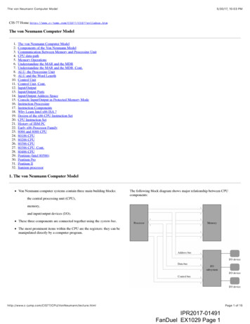
The von Neumann Computer Model5/30/17, 10:03 PMCIS-77 Home http://www.c-jump.com/CIS77/CIS77syllabus.htmThe von Neumann Computer 19.20.21.22.23.24.25.26.27.28.29.30.31.32.The von Neumann Computer ModelComponents of the Von Neumann ModelCommunication Between Memory and Processing UnitCPU data-pathMemory OperationsUnderstanding the MAR and the MDRUnderstanding the MAR and the MDR, Cont.ALU, the Processing UnitALU and the Word LengthControl UnitControl Unit, Cont.Input/OutputInput/Output PortsInput/Output Address SpaceConsole Input/Output in Protected Memory ModeInstruction ProcessingInstruction ComponentsWhy Learn Intel x86 ISA ?Design of the x86 CPU Instruction SetCPU Instruction SetHistory of IBM PCEarly x86 Processor Family8086 and 8088 CPU80186 CPU80286 CPU80386 CPU80386 CPU, Cont.80486 CPUPentium (Intel 80586)Pentium ProPentium IIItanium processor1. The von Neumann Computer ModelVon Neumann computer systems contain three main building blocks:The following block diagram shows major relationship between CPUcomponents:the central processing unit (CPU),memory,and input/output devices (I/O).These three components are connected together using the system bus.The most prominent items within the CPU are the registers: they can bemanipulated directly by a computer /lecture.htmlPage 1 of 15IPR2017-01491FanDuel EX1029 Page 1
The von Neumann Computer Model5/30/17, 10:03 PM2. Components of the Von Neumann Model1. Memory: Storage of information (data/program)The von Neumann Machine:2. Processing Unit: Computation/Processing of Information3. Input: Means of getting information into the computer. e.g. keyboard,mouse4. Output: Means of getting information out of the computer. e.g. printer,monitor5. Control Unit: Makes sure that all the other parts perform their taskscorrectly and at the correct time.3. Communication Between Memory and Processing UnitCommunication between memory and processing unit consists of two registers:Memory Address Register (MAR).Memory Data Register (MDR).To read,1. The address of the location is put in MAR.2. The memory is enabled for a read.3. The value is put in MDR by the memory.To write,1. The address of the location is put in MAR.2. The data is put in MDR.3. The Write Enable signal is asserted.4. The value in MDR is written to the location nn/lecture.htmlPage 2 of 15IPR2017-01491FanDuel EX1029 Page 2
The von Neumann Computer Model5/30/17, 10:03 PM4. CPU data-pathHardware units like ALU's, registers, memory, etc., are linked togetherinto a data-path.The flow of bits around the data-path is controlled by the "gates" whichallow the bits to flow (on) or not flow (off) through the data-path.The binary instructions (1 on; 0 off) that control the flow are calledmicro-instructions.Simplified x86 data path :5. Memory OperationsThere are two key operations on memory:Memory ann/lecture.htmlPage 3 of 15IPR2017-01491FanDuel EX1029 Page 3
The von Neumann Computer Model5/30/17, 10:03 PM1. fetch( address ) returns value without changing the value stored atthat address.2. store( address, value ) writes new value into the cell at the givenaddress.This type of memory is random-access, meaning that CPU can access anyvalue of the array at any time (vs. sequential access, like on a tape).Such memories are called RAM (random-access memory.)Some memory is non-volatile, or read-only (ROM or read-only memory.)6. Understanding the MAR and the MDRMAR stands for memory address register:Memory Circuitry:MAR is connected to the address bus.MAR is "the only way" for the CPU to communicate with address bus.Tri-state buffer between MAR and the address bus prevents MAR from continouslydumping its output to the address bus.MAR can hold either an instruction address or a data address.7. Understanding the MAR and the MDR, Cont.MDR Stands for memory data register.Memory Circuitry:MDR is connected to the data bus.Data can go in both directions: to and from memory,therefore, MDR can load its data fromthe data bus (for reading data)one of the CPU registers (for storing data.)A 2-1 MUX circuit selects input from one of the two.More info: von Neumann Architecture article by Prof. Fabio Pellacini, Dartmouth College, ure.htmlPage 4 of 15IPR2017-01491FanDuel EX1029 Page 4
The von Neumann Computer Model5/30/17, 10:03 PM8. ALU, the Processing UnitProcessing unit is hardware that implements Arithmetic and LogicalOperations.The ALU:ALU stands for Arithmetic and Logic Unit, capable of performingADD, SUBTRACT, AND, OR, and NOToperations.The size of input quantities of ALU is often referred to as word length of the computer.Many processors today have word length of 32 and 64 bit.Processing unit also includes a set of registers for temporary storage of data and memory addressing.9. ALU and the Word LengthThe size of quantities processed by ALU is the word length of the computer.The word length does not affect what a computer can compute.A computer with a smaller word length can do the same computation as one with a larger word length.but it will take more time.For example, to add two 64 bit numbers,word length 16 takes 4 adds.word length 32 takes 2 adds.word length 64 takes 1 add.10. Control UnitManages the Precessing Unit.Implemented as FSM.FSM directs all activity.Clock-based step-by-step precessing, cycle-by-cycle.FSM is controlled by the1. Clock signal2. Instruction Register3. Reset ecture.htmlPage 5 of 15IPR2017-01491FanDuel EX1029 Page 5
The von Neumann Computer Model5/30/17, 10:03 PM11. Control Unit, Cont.Control unit includesInstruction Register IRInstruction Pointier IP (aka Program Counter PC)FSM outputs of the control unit,- - - - - shown by dash lines, have two purposes:1. Control processing that takes place inside the ALU.2. Authorize read/write gate control of the CPU data-path.Control unit demo: cjumpcxx.exe - CPU, memory, Assembly - Protected memory.12. Input/OutputI/O controller provides the necessary interface to I/O devices.Takes care of low-level, device-dependent details.Provides necessary electrical signal nn/lecture.htmlPage 6 of 15IPR2017-01491FanDuel EX1029 Page 6
The von Neumann Computer Model5/30/17, 10:03 PM13. Input/Output PortsProcessor and I/O interface points for exchanging data are called I/O ports.Two ways of mapping I/O ports:1. Memory-mapped I/O:I/O ports are mapped to the memory address space.Reading/writing I/O is similar to reading/writing memory.Can use memory read/write instructions.Motorola 68000 uses memory-mapped I/O.2. Isolated I/O:Separate I/O address space.Intel 80x86 processors support isolated I/O.Requires special I/O instructions, like IN and OUT on x86.14. Input/Output Address SpacePentium x86 provides 64 KB of I/O address space.Can be used for 8-, 16-, and 32-bit I/O ports.Combination cannot exceed the total I/O address space, can have either64 K 8-bit ports32 K 16-bit ports16 K 32-bit cture.htmlPage 7 of 15IPR2017-01491FanDuel EX1029 Page 7
The von Neumann Computer Model5/30/17, 10:03 PMA combination of these for a total of 64 KB.I/O instructions do not go through memory segmentation or paging.I/O address refers to the physical I/O address.15. Console Input/Output in Protected Memory ModeUsing console in Protected Memory Mode:Von Neumann Computer System Block Diagram:Keyboard inputConsole display outputAscii character encoding16. Instruction ProcessingCentral idea of von Neumann model is that both program and data stored in computer memory:Program is a sequence of instructionsInstruction is a binary encoding of operations and operands:For example, an arithmetic expression-a b * ccould be computed by a program with three machine instructionsneg aximul bx, cxadd ax, bx; negate (multiply by -1); multiply and store result in bx; add and store result in axwhere NEG, IMUL, ADD are arithemtic instructions, AX, BX, and CX are operands.Instructions are most basic units of processing.Instructions are executed under control of the control unit.17. Instruction ComponentsInstruction in memory has two parts: opcode and operands.Instruction formats:The opcode identifies the operation that instruction doesThe operands are subjects of the operation, such as data values, registers, or nNeumann/lecture.htmlPage 8 of 15IPR2017-01491FanDuel EX1029 Page 8
The von Neumann Computer Model5/30/17, 10:03 PMDue to variety of opcodes and operands, instructions may occupy different sizes ofbytes in memory.Instructions with no operands can have implied operands, those that are not explicitlyshown.18. Why Learn Intel x86 ISA ?The x86 Intel CPU family is generally classified as a Von Neumann Architecture Machine.Most pervasive ISA in the marketplace.Opcodes have zero or more operands.Instructions and operands have strong support for data types.All x86 Assemblers are free, including Microsoft Macro Assembler, MASM.Fullscreen 32-bit debuggers WinDbg, OllyDbg, and MS Visual Studio.19. Design of the x86 CPU Instruction SetInstruction set architecture (ISA) is an important design issue for CPU designers:caches, pipelining, superscalar implementation can be added to the design later, butit is very difficult to change the CPU instructions once in production and people writing software.LOOP instruction on the x86 CPU sees very little use in modern high-performance programs.Challenges:Expandability is a big concern (predicting future needs.)Legacy support is almost the opposite of expandability.Each instruction requires some number of transistors on the CPU's silicon die.20. CPU Instruction SetA typical Von Neumann architecture encodes CPU instructions as numeric values in memory.Instruction decoder:Programming and engineering of the instruction set is a major task in the CPU design.Each instruction needs a unique numeric opcode.Instruction /lecture.htmlPage 9 of 15IPR2017-01491FanDuel EX1029 Page 9
The von Neumann Computer Model5/30/17, 10:03 PM21. History of IBM PCDesign a simple instruction set to begin with and leave room for later expansion main reason the x86 is so popular and long-lived.Intel started with a relatively simple CPU and figured out how to extend the instruction set to accommodate new features.IBM decided that open documentation is a good thing.IBM published the IBM PC Technical Reference Manual, with everything the engineers knew about the machine, which was another reason for the successof the IBM PC platform.See also: 25 Years of the IBM PC and CNN article Meet the inventor of Ctrl-Alt-Delete22. Early x86 Processor FamilyIntel introduced microprocessors in 1969: 4-bit microprocessor 4004.8-bit microprocessors are 8080 and 8085 models.16-bit processors:8086 introduced in 1979.20-bit address bus, 16-bit data bus.(8088 is a less expensive version.)Uses 8-bit data bus.Can address up to 4 segments of 64 KB.Referred to as the real mode addressing.Still fully compatible with modern x86 ecture.htmlPage 10 of 15IPR2017-01491FanDuel EX1029 Page 10
The von Neumann Computer Model5/30/17, 10:03 PM23. 8086 and 8088 CPUYear 1979The 8088, 8086, and 80286 are 16-bitCPUs.Internal registers are 16 bits in size.The 8086 is faster than the 8088because of its 16-bit data bus; the 8088has only an 8-bit data bus.The 16-bit data bus allows you to useEVEN and ALIGN on an 8086processor to word-align data and thusimprove data-handling efficiency.Memory addresses on the 8086 and8088 refer to actual physical addresses.The 8086 and 8088 have 20 addresspins, and 1 megabyte of addressablememory (which is the real modesegmented memory explained later)requires addresses of 20 bits in size.See also: Brief History ofMicroprocessors24. 80186 CPUA faster version of 8086.16-bit data bus and 20-bit address bus.Improved instruction set.25. 80286 CPUYear 1982.Introduced protected mode addressing.Enhanced with memory protection capabilities with some instructions to control protected mode.Runs faster.24-bit address bus.16 MB address ecture.htmlPage 11 of 15IPR2017-01491FanDuel EX1029 Page 11
The von Neumann Computer Model5/30/17, 10:03 PMSegmentation in protected mode is different from the real mode.Allows the operating system to run multiple processes at the same time.The 80286 was the minimum for running Windows 3.1 and higher.Backwards compatible.26. 80386 CPUYear 1985.The 80386 and many of its successors are 32-bit CPUs.Internal registers are 32 bits in size.Unlike its predecessors, the 80386 processor can handle both 16-bit and 32-bit data.Supports entire instruction set of 80286.Adds several new instructions as well.Software written for the 80286 runs unchanged on the 80386, but the chip is faster.The 80386 implements many new hardware-level features, includingpaged memory.segmentation can be turned off (flat model).support for multiple virtual 8086 processes.addressing of up to 4 gigabytes of memory.specialized debugging registers.27. 80386 CPU, Cont.32 bit operating systems such as Windows NT required 80386 or higher processor.More embedded systems nowdays use the 80386 CPU.Examples include:high speed data communications devices.graphics equipment.tra-high-speed data acquisition gear.Cockpit displays of some modern jetliners use 80386 as controllers.See also: Intel 386 Manuals28. 80486 CPUYear 1989.The 80486 processor is an enhanced version of the 80386 withinstruction pipelining allows parallel execution capability to instruction decode and execution units.executes many instructions 2-3 times faster.achieves scalar execution of 1 instruction per clock ecture.htmlPage 12 of 15IPR2017-01491FanDuel EX1029 Page 12
The von Neumann Computer Model5/30/17, 10:03 PMThe chip incorporatesmath coprocessor for performing floating-point arithmetic8 Kilobyte memory cache.(The math coprocessor was disabled on a variation of the chip called the 80486SX.)New instructions.Fully compatible with 80386 software.Later versions introduced energy savings for laptops.See also: Intel 486 Manuals29. Pentium (Intel 80586)Pentium was introduced in 1993, followed byPentium Pro in 1995,Pentium II in 1997,Pentium III in 1999,Pentium IV 2001.Similar to 80486 but with 64-bit data bus.Wider internal datapaths: 128- and 256-bit wide.Added second execution pipeline.Superscalar performance allows two instructions per clock cycle.Doubled on-chip level-1 cache:one 8 KB for dataanother 8 KB for instructions.Added branch ann/lecture.htmlPage 13 of 15IPR2017-01491FanDuel EX1029 Page 13
The von Neumann Computer Model5/30/17, 10:03 PMSee also: Pentium Manuals30. Pentium ProIntroduced in 1995.Three-way superscalar performance, 3 instructions per clock cycle.36-bit address bus.64 GB address space.Introduced dynamic execution:Out-of-order execution.Speculative execution.In addition to the level-1 cache, has 256 KB level-2 cache.31. Pentium re.htmlPage 14 of 15IPR2017-01491FanDuel EX1029 Page 14
The von Neumann Computer Model5/30/17, 10:03 PMIntroduced in 1997.Added multimedia (MMX) instructions.Doubled on-chip level-1 cache:16 KB for data16 KB for instructions.Introduced comprehensive power management features:SleepDeep sleep.In addition to the level-1 cache has 256 KB level-2 cache.32. Itanium processorRISC design(All previous x86 designs were CISC.)64-bit processorUses 64-bit address bus128-bit data busIntroduced several advanced features:Speculative executionPredication to eliminate branchesBranch nn/lecture.htmlPage 15 of 15IPR2017-01491FanDuel EX1029 Page 15
Von Neumann Computer System Block Diagram: 16. Instruction Processing Central idea of von Neumann model is that both program and data stored in computer memory: Program is a sequence of instructions Instruction is a binary encoding of operations and operands: For example, an arithmetic expression-a b * c