Transcription
Mechanism of Low Temperature ALD of Al2O3 on Graphene TerracesIljo Kwaka,b, Jun Hong Parka,b, Larry Grissomc, Bernd Fruhbergerc, Andrew C, KummelbaMaterials Science and Engineering Program, University of California, San DiegoDepartment of Chemistry and Biochemistry, University of California, San DiegocCalifornia Institute for Telecommunications and Information Technology, University ofCalifornia San DiegobUniform and defect-free Al2O3 films were grown on highlyoriented pyrolytic graphite (HOPG) terraces by thermal atomiclayer deposition (ALD) at low temperature (50 oC) without anyfunctionalization of the surface. Controlling the pulse times oftrimethylaluminum (TMA) and H2O while using short Ar purgetimes, 1-2 nanometer size Al2O3 particles were formed on theHOPG terraces. The particles provided a layer of nanoscalenucleation centers on the HOPG terraces. Capacitance-voltagemeasurements of Al2O3 films grown at 50 oC using 50 ALD cyclesshowed an areal capacitance 1.17 F/cm2 with very smallfrequency dispersion, consistent with the absence of inductioncycles and formation of a high quality interface. The leakagecurrent of the Al2O3 was 10-5 A/cm2 in large area devices(1900 m2) which is comparable with results from devicesprepared using an identical ALD process for Al2O3 onSi0.7Ge0.3(001) substrates, and is consistent with the absence ofpinholes.IntroductionSince its emergence in 2004 (1,2), single layer graphene has attracted attentiondue to its high mobility of charge carriers and charge confinement. Graphene has beenviewed as a viable alternative channel material for future logic transistors becausetransistors based on silicon are approaching their fundamental limits.(3,4) However, inorder to fabricate graphene devices, deposition of ultrathin, pinhole-free high-k dielectricgates is required. Atomic layer deposition (ALD) is the most effective method to depositultrathin high-k dielectric layers, due to excellent thickness control.(5) However, becauseof the inert nature of graphene surfaces, similar to the surfaces of carbon nanotubes(CNTs), conventional ALD dielectric layers selectively nucleate on defect sites or stepedges.(6,7) In the conventional ALD process on graphene, such non-uniform oxidesresult in large leakage currents in devices.(8)For CNTs, Farmer et functionalized the surface of CNTs using nitrogen dioxide(NO2) and trimethylaluminum (TMA) at 25 oC to form an Al2O3 layer by ALD; however,the induction period for onset of uniform film growth was 100 ALD cycles.(9) Similarly,
several methods have been used to functionalize graphene surfaces including chemicaltreatment, deposition of oxidizing metal films, and polymer based seeding layers.(10, 11,12, 13) Unfortunately, these functionalization methods can result in degradation of theelectronic properties of graphene or require thick dielectric layers. Therefore, forsuccessful fabrication of graphene devices, improved techniques for deposition ofuniform and insulating gate oxides continue to be needed.In this work, Al2O3 was directly deposited on highly oriented pyrolytic graphite(HOPG) surfaces by low temperature thermal ALD using TMA and H2O without anyseeding layer or surface treatments prior to deposition. With the substrates at atemperature of 50 oC, using short purge times between the two precursor pulses and longpulses of the precursors, a CVD growth component was intentionally employed toprovide more nucleation sites on the surface. The CVD growth component inducesformation of 1-2 nanometer Al2O3 particles on the surface which provide nucleationcenters for uniform deposition. The deposited Al2O3 film was continuous and uniformwithout observable defects. The surface morphology of the oxide was analyzed by atomicforce microscopy (AFM) and electrical properties were characterized by capacitancevoltage and leakage current measurements of metal/Al2O3/HOPG stacks.Experimental TechniquesHOPG samples (from SPI supplies) were cleaned by the mechanical exfoliationmethod using an adhesive tape. The samples were loaded into a commercial ALD reactor(Beneq TFS 200 ALD system) which has a hot wall, crossflow reaction chamber. Thereaction chamber was pumped down to 1 mTorr. To deposit Al2O3, TMA and H2O wereused as ALD precursors, temperature stabilized at 20 oC. The carrier gas was researchpurity argon (Ar, Praxair, 99.9999%) which was flowed at 300 sccm (standard cubiccentimeter). 50 cycles of ALD were employed, each cycle consisting of a sequence of600 ms TMA pulse, 500 ms Ar purge, 50 ms H2O pulse, and 500 ms Ar purge. Forcomparison, using identical ALD pulse times, films were grown with sampletemperatures between 50 oC to 200 oC to investigate the effect of temperature on thenucleation of Al2O3. To compare nucleation behavior on a highly reactive substrate,Al2O3 was deposited on Si0.7Ge0.3(001) substrates using 50 cycles of ALD, consisting ofsequences of 300 ms or 400 ms TMA pulses followed by 50 ms H2O pulses with 500 msAr purge at 50 oC sample temperature. In addition, the effect of the precursor pulse timeson the morphology of the oxide on HOPG were studied. TMA and H2O pulse durationswere changed from 200 ms to 600 ms and 50 ms to 150 ms, respectively, while thesample temperature during ALD was fixed at 50 oC.After the ALD process, non-contact mode AFM measurements were performed todetermine the correlation between the surface topography and the ALD conditions. MIM(Metal-Insulator-Metal) capacitors were fabricated to characterize the electricalproperties of the oxide. In order to compare the quality of the oxide, Si0.7Ge0.3 substrateswere loaded along with the HOPG samples. Al2O3 was deposited on HOPG andSi0.7Ge0.3(001) using 50 cycles of ALD with the samples at 50 oC. After the ALD process,Ni gates were deposited on the oxide by thermal evaporation. The gates were 50 m indiameter and 3 nm thick. As a control, Ni/Al2O3/Si0.7Ge0.3/Al metal–oxide–
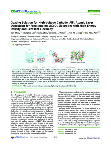
semiconductor capacitors (MOSCAPs) were also fabricated with a slightly differentprocess due to different cleaning and contact requirements. Prior to ALD, eachSi0.7Ge0.3(001) sample was treated with a 30 s rinse by each of acetone, isopropyl alcohol,and DI water followed by N2 drying. Afterwards, the native oxide was removed by cyclicHF cleaning using a 2% HF solution and DI water at 25 oC for 1 min in each solution for2.5 cycles.(14) For each SiGe sample, 50 cycles of ALD deposition were followed by Nigate deposition and 100-nm thick Al back contact deposition using DC sputtering. Forboth the HOPG and SiGe samples, the capacitance-voltage curves were measured in thefrequency range of 2 kHz to 1MHz at room temperature with an HP4284A LCR meter.Leakage current of current of the oxide was obtained in the range of -2V to 2V.Results and DiscussionTemperature dependence of Al2O3 ALDFigure 1. (Color) AFM images of Al2O3 films (50 ALD cycles) on HOPG withdifferent sample growth temperatures. (a) 200 oC, (b) 150 oC and (c) 50 oC. Each ALDcycle consisted of a 600 ms TMA pulse, 500 ms Ar purge, 50 ms H2O pulse, and 500 msAr purge. (d) 50 ALD cycles of Al2O3 were deposited with 2 s purge times at sampletermperature of 50 oC, using otherwise identical ALD conditions as for the samples in (a),(b), (c). Non-contact mode AFM measurements were carried out with a Si tip. Note thatfor high temperature ALD, the nucleation of Al2O3 was only observed along the stepedges while for low temperature ALD, the nucleation was observed across the terracesand the step edges. In addition, for low temperature ALD, 1-2nm spheres were observedon the surface. The size of each image is 2x2 m2.
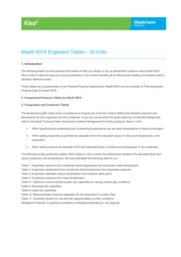
Figure 1 shows AFM images of Al2O3 grown on HOPG using 50 cycles of ALDat sample temperatures of 200 oC, 100 oC, and 50 oC. Each ALD cycle for the samples ofFigs. 1(a),(b),(c) consisted of 600 ms TMA pulse and 50 ms H2O pulse, with 500 ms Arpurge times between precursor pulses. The growth of Al2O3 exhibited strong dependenceon sample temperature. As shown in Figs. 1 (a) and (b), when the sample temperaturewas above 100 oC, Al2O3 was only deposited on the step edges of the HOPG and not onthe terraces, because dangling bonds for nucleation are only available on the step edgesand not on the inert terraces. The thickness of the Al2O3 deposited on the step edges wasabout 5 nm which is consistent with the expected thickness for 50 cycles of ALD at thetypical 0.1 nm/cycle ALD growth rate.(15)When the sample temperature was decreased to 50 oC as shown in Fig. 1(c), theAl2O3 film was deposited continuously on both the step edges and the terraces withoutpin hole formation. Spherical Al2O3 features were observed across the entire surfaces forthe growth at 50 oC sample temperature. However, these features are only observed witha short purge time between two precursor pulses at 50 oC sample temperature. When thepurge time was increased to 2s with identical precursor ALD pulse times and sampletemperature, the spherical Al2O3 features were not observed as shown in Fig 1(d). Shortpurge times can induce a chemical vapor deposition (CVD) growth component sinceexcess unreacted physisorbed precursor molecules have insufficient time to desorb fromboth the substrate and chamber walls during the short purge time. The CVD componentinduced deposition of particles of about 2 0.4 nm diameter which was quantified byaveraging 10 AFM line scans. Al2O3 particles on the surface were formed by eithernucleation in the ALD chamber and subsequently transported to the sample surface orwere formed by precursor islands on the surface. Since surface island growth is usuallynon-spherical and similar nuclei were also observed on the reactive SiGe surface (Fig2(a),(b)), the data is most consistent with nuclei formation in the ALD chamber (denotedgas phase nucleation below).(16, 17)Figure 2. (Color) AFM images of Al2O3 films (50 ALD cycles) on Si0.7Ge0.3(001)grown at 50 oC sample temperature. ALD was carried out using sequences of (a)300 ms TMA pulse and 50 ms H2O pulse with 500 ms of Ar purge after each precursorpulse, (b) 400 ms TMA pulse and 50 ms H2O pulse with 500 ms of Ar purge after eachprecursor pulse at 50 oC sample temperature. Spherical Al2O3 nuclei were observed onSiGe (white dots). This data is consistent with nuclei formation in the ALD chamber. Thesize of each image is 2x2 m2.
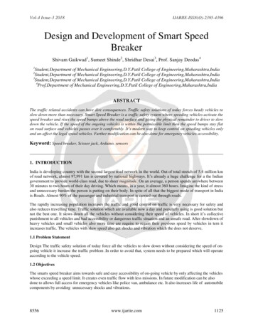
Effect of precursor pulse time on Al2O3 ALDFigure 3 (a)-(c) shows the AFM images of Al2O3 grown by ALD at 50 oC sampletemperature with different pulse lengths of TMA and H2O with a fixed Ar purge time of500 ms. For the sample with 200 ms TMA pulses and 50 ms H2O pulses (Fig. 3(a)),Al2O3 was mainly deposited on the step edges. Although some Al2O3 was nucleated onthe terraces, it was discontinuous with a high density of visible pinholes. The numberdensities of the Al2O3 particles (number of particles per 4 m2 image area) with the threedifferent ALD conditions are shown in Table I. For the sample shown in Fig. 3(a), grownusing relatively short 200 ms TMA pulses, the density of the Al2O3 particles (15/ m2)was significantly lower than for the samples shown in Figs. 3(b),(c), which were grownunder different conditions with longer TMA pulse times. When the TMA pulse time wasincreased to 600 ms while fixing the H2O pulse length (Fig. 3(b)), the density of theAl2O3 particles was markedly increased (123/ m2) and continuous Al2O3 films weredeposited on both terraces and step edges without pinholes. AFM line traces show thatthe particles are 2 0.6 nm in diameter (Fig 3(e)). The observation of the high density ofdefects and low density of Al2O3 particles in the dielectric deposited using short TMApulses indicates that the Al2O3 particles have a critical role in the formation of uniformdielectric layers on HOPG during ALD.Figure 3. (Color) AFM images of Al2O3 films (50 ALD cycles) on HOPG (a) 200 msTMA and 50 ms H2O pulses, (b) 600 ms TMA and 50 ms H2O pulses, and (c) 600 msTMA and 150 ms H2O pulses. (d), (e), and (f) are AFM height profiles along the yellowlines in Figs. (a), (b) and (c) respectively. For the ALD with short pulses ((a), (d)), fewcondensation nuclei were observed, and the ALD nucleation primarily occurred on thestep edges. For the two samples grown with longer TMA pulses ((b), (e) and (c), (f)),white condensation nuclei were distributed across the terraces, and ALD nucleationoccurred on both the terraces and the step edges.
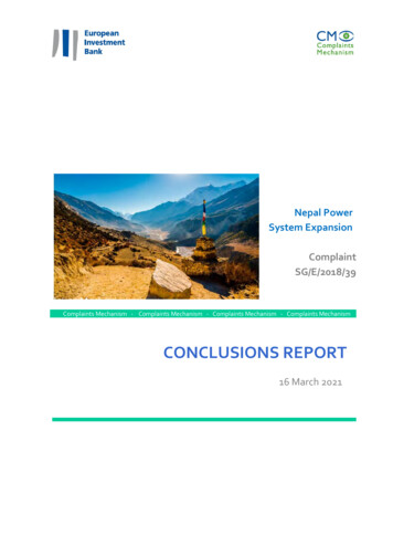
When the H2O pulse time was increased to 150 ms with a fixed TMA pulse timeof 200 ms (Fig. 3(c)), similar morphology as for the growth with a long TMA pulse (Fig.3(b)) was observed. The Al2O3 film was continuous with a high density of Al2O3 particles(44/ m2). AFM lines traces (Fig. 3(f)) show the particles increased in size to 4 0.7 nm.This indicates that the Al2O3 particles were formed by a CVD component that can becontrolled by the TMA and H2O pulse times. This observation is consistent with both theisland formation mechanism and the gas phase formation mechanism for the particles.TABLE I. Number density of Al2O3 particles from films grown with differentALD conditions (Number of particles per 4 m2)200 ms TMA &50 ms H2O pulses600 ms TMA &50 ms H2O pulses200 ms TMA &150 ms H2O pulses59692176Electrical PropertiesMIM capacitors were fabricated on freshly cleaved HOPG substrates. Al2O3 filmswere deposited using 50 ALD cycles consisting of 600ms TMA pulse, 500 ms Ar purge,50 ms H2O pulse, and 500 ms Ar purge at 50 oC sample temperature. Subsequently, Nimetal gates were deposited by thermal evaporation. The area of the capacitor was 1900 m2 (50 m diameter). Capacitance-voltage (C-V) and leakage current-voltage (IV) measurements were performed in order to evaluate the electrical quality of the oxide.As shown in Fig. 4(a), the capacitance of the oxide was nearly independent of the appliedvoltage owing to the MIM structure of the capacitor. Previously, Park et al reported fullymodulated capacitance of Al2O3/monolayer TiOPc/graphene stacks.(18) For single layergraphene, capacitance can be modulated near 0 V due to the linear dispersion of thedensity of states near the Fermi energy level. However, because of the high charge carrierdensity of HOPG near the Fermi energy level, the modulation of capacitance was notobserved. The Cmax of the oxide was 1.17 F/cm2 which is consistent with the Cmax valueof the ALD grown Al2O3 on Si0.7Ge0.3(001) as shown in Fig. 4(b). This indicates thatdeposition of Al2O3 on HOPG proceeded without an ALD induction time. Note the highdispersion of the C-V data on Si0.7Ge0.3 was likely due to the formation of GeOx whichcan be suppressed by (NH4)2S(aq) or NH3 plasma treatments.(19, 20) However, thesecleaning recipes were not employed in this study since they may induce unintentionalchemical changes of HOPG and degradation of the surface quality on HOPG.
Figure 4. (Color) Comparison of Electrical Properties of Low Temperature Al2O3ALD on HOPG and Si0.7Ge0.3(001) with cycles consisting of a 600 ms TMA pulse,500 ms Ar purge, 50 ms H2O pulse, and 500 ms Ar purge at 50 oC sampletemperature.(a) Capacitance vs. Voltage Curve of Ni/Al2O3(50 ALD cycles)/HOPGstack. (b) Capacitance vs. Voltage Curve of Ni/ Al2O3(50 ALD cycles)/Si0.7Ge0.3/Al stack.(c) I-V curve of Ni/ Al2O3(50 ALD cycles)/HOPG and Ni/ Al2O3(50 ALDcycles)/Si0.7Ge0.3/Al stack. The similar Cox on HOGP and Si0.7Ge0.3(001) is consistentwith no ALD induction cycles on HOPG. The comparable leakage currents ofAl2O3/HOPG to Al2O3/Si0.7Ge0.3 are consistent with the oxide on HOPG being uniformand pin-hole free on the HOPG substrate.Figure 4 (c) compares the leakage currents of Al2O3 films grown by 50 ALDcycles on HOPG (red) and Si0.7Ge0.3(001) (blue) substrates. ALD was performedsimultaneously at 50 oC sample temperature on the two substrates. The leakage current ofthe oxide on the HOPG was 3.1 10-5 A/cm2 and 2.2 10-6 A/cm2 for the Si0.7Ge0.3 at -1 V.The low leakage on Si0.7Ge0.3 is expected since Al2O3 readily nucleates on Si0.7Ge0.3(001),and the Si0.7Ge0.3(001) surface is flat without bunched steps. Conversely, HOPG surfacesare inert and have bunched steps.(16, 18) The leakage current of the ALD grown Al2O3on HOPG at 50 oC sample temperature being within 15x of the leakage current onSi0.7Ge0.3(001) is consistent with the oxide on HOPG being uniform and pin-hole free onthe HOPG substrate.ConclusionDeposition of high quality Al2O3 films on HOPG was demonstrated by lowtemperature ALD without evidence for an ALD induction period prior to onset ofuniform film growth. Controlling the pulse times of TMA and H2O along with a shortpurge time, 1-2 nanometer diameter spherical Al2O3 particles were formed on bothHOPG and SiGe consistent with a gas phase reaction of the ALD precursors. The nucleiprovided uniform nucleation centers on the inert HOPG surface resulting in uniform andpin-hole free Al2O3 films on both step edges and terraces. Comparable Cox for lowtemperature ALD grown Al2O3 on HOPG and Si0.7Ge0.3(001) is consistent with theabsence of induction cycles even on the inert HOPG surface. The leakage current of theAl2O3 was as low 10-5 A/cm2 which is within 15x of the leakage current observed for
Al2O3 on highly recative Si0.7Ge0.3(001) substrates. This work has great potential forfabrication of novel graphene-based devices.AcknowledgmentsThis work is supported in part by the National Science Foundation Grant DMR1207213, by the Center for Low Energy Systems Technology (LEAST), a STARnetSemiconductor Research Corporation (SRC) program sponsored by MARCO andDARPA, and by the SRC Nanoelectronic Research initiated through the South WestAcademy of Nanoelecronics (SWAN). Experiments were performed in the UCSD Nano3facility supported by the NNCI (ECCS-1542148).References1. K. S. Novoselov, A. K. Geim, S. V. Morozov, D. Jiang, Y. Jiang, S. V. Dubonos,I. V. Grigirieva, and A. A. Firsov, Science, 306, 666 (2004).2. K. S. Novoselov, A. K. Geim, S. V. Morozov, D. Jiang, M. I. Katsnelson, I. V.Grigorieva, S. V. Dubonos, and A. A. Firsov, Nature (London), 438, 197 (2005).3. D. Alamo, J. A. Nature 479.7373 (2011).4. Y. Xuan, Y.Q. Wu, P. D. Ye, Electron Device Letters, IEEE 29.4 (2008)5. R.L. Puurunen, J. Appl. Phys. 97, 121301 (2005)6. Y. Xuan1, Y. Q. Wu1, T. Shen1, M. Qi1, M. A. Capano1, J. A. Cooper1 and P. D.Ye, Birck and NCN Publications (2008)7. X Wang, SM Tabakman and H Dai,,Journal of the American Chemical Society130.26 (2008)8. W. Y. Fu, L. Liu, W.L. Wang, M. H. Wu, Z. Xu, X. D. Bai and E. G. Wang,Science China Physics, Mechanics and Astronomy 53, no. 5 (2010)9. D. B. Farmer, and R. G. Gordon, Nano letters 6, no.4 (2006)10. M. J. Hollander, M. LaBella, Z. R. Hughes, M. Zhu, K. A. Trumbull, R. Cavalero,D. W. Snyder, X. Wang, E, Hwang, S. Datta, and J. A. Robinson, Nano letters 11.No. 9 (2011)11. B. Fallahazad, B., K. Lee, G. Lian, S. Kim, C. M. Corbet, D. A. Ferrer, L.Colombo, and E. Tutuc, Applied Physics Letters 100, no. 9 (2012)12. S. S. Tinchev, Applied Surface Science 258.7 (2012)13. B. Lee, S. Y. Park, H. C. Kim, K. J. Cho, E. M. Vogel, M. J. Kim, R. M. Wallace,and J. Kim, Applied Physics Letters 92, no. 20 (2008)14. O. Yasuhiro, M. Shandalov, Y. Sun, P. Pianetta, and P. C. McIntyre. AppliedPhysics Letters 94, no. 18 (2009)15. Y, Kim, S. M. Lee, C.S. Park, S.I. Lee, M.Y. Lee, Applied Physics Letters 71(1997): 3604-3606.16. M. Volmer and A. Weber, Z. phys. Chem 119.3/4 (1926)17. M. Volmer and A. Weber. Nucleation in super-saturated products (1988).18. J.H. Park, H. C. Movva, E. Chagarov, K. Sardashti, H. Chou, I. Kwak, K. T. Hu,S. K. Fullerton-Shirey, P. Choudhury, S. K. Banerjee, A. C. Kummel, Nanoletters 15, no. 10 (2015)
19. K. Sardashti K, K. T. Hu, K. Tang, S. Park, H. Kim, S. Madisetti, P. McIntyre, S.Oktyabrsky, S. Siddiqui, B. Sahu, N. Yoshida, J. Kachian and A. C. Kummel,Interfaces. Applied Surface Science. (2016)20. K. Sardashti, K. T. Hu, K. Tang, S. Madisetti, P. McIntyre, S. Oktyabrsky, S.Siddiqui, B. Sahu, N, Yoshida, J. Kachian, B. Fruhberger and A. C. Kummel,Applied Physics Letters 108, no. 1 (2016)
In this work, Al 2 O 3 was directly deposited on highly oriented pyrolytic graphite (HOPG) surfaces by low temperature thermal ALD using TMA and H 2 O without any seeding layer or surface treatments prior to deposition. With the substrates at a temperature of 50 oC, using short purge times between the two precursor pulses and long


