Transcription
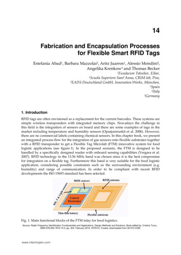
14Fabrication and Encapsulation Processesfor Flexible Smart RFID TagsEstefania Abad1, Barbara Mazzolai2, Aritz Juarros1, Alessio Mondini2,Angelika Krenkow3 and Thomas Becker1Fundacion Tekniker, Eibar,Superiore Sant’Anna, CRIM lab, Pisa,3EADS Deutschland GmbH, Innovation Works, München,1Spain2Italy3Germany2Scuola1. IntroductionRFID tags are often envisioned as a replacement for the current barcodes. These systems aresimple wireless transponders with integrated memory chips. Nowadays the challenge inthis field is the integration of sensors on board and there are some examples of tags in themarket including temperature and humidity sensors (Opasjumruskit et al. 2006). However,there are no commercial labels containing chemical sensors. In this chapter book, we presentan integrated process flow for the integration of gas sensors onto flexible substrates togetherwith a RFID transponder to get a Flexible Tag Microlab (FTM) innovative system for foodlogistic applications (see figure 1). In the proposed scenario, the FTM is designed to behandled by a specifically designed reader with onboard sensing capabilities (Vergara et al.2007). RFID technology in the 13.56 MHz band was chosen since it is the best compromisefor integration on a flexible tag. Furthermore this band is very suitable for the food logisticapplication, considering possible constraints such us the surrounding environment (e.g.humidity) and range of communication. In order to be compliant with recent RFIDdevelopments the ISO 15693 standard has been selected.Fig. 1. Main functional blocks of the FTM inlay for food logistics.Source: Radio Frequency Identification Fundamentals and Applications, Design Methods and Solutions, Book edited by: Cristina Turcu,ISBN 978-953-7619-72-5, pp. 324, February 2010, INTECH, Croatia, downloaded from SCIYO.COMwww.intechopen.com
238Radio Frequency Identification Fundamentals and Applications, Design Methods and SolutionsThis visionary application involves both the fabrication of the so-called inlay, which is theflexible substrate, acting mainly as a passive interconnect structure, with all componentsneeded for the FTM assembled on it, and the development of particular assembly andpackaging issues for the new ultra-low power consumption substrates for gas sensorintegration.Flexible substrate, microcomponents assembly and encapsulation technologies have beenused throughout the electronics industry and continue to play a major role in new designsand applications. Flexible substrate technologies refer to a group of processes for theconstruction of multi-layer flexible circuits, commonly based on the use of a polyimide asraw material. Typical fabrication of this type of circuit involves the masking and etchingmethods similar to those employed by printed circuit board manufacturers. The componentassembly techniques have been developed to perform a hybrid integration of flexiblesubstrates with integrated electronic circuitry on bare dice. Flip chip bond, wire bond,electrically conductive glues and tapes are some examples of connection methods.Envisioned miniaturized systems could be assembled by combining these techniques andsolder steps. There is virtually no limit to the types of terminations possible for flexiblecircuits. Wire, cable, contacts, printed circuit boards, chips and microstructures can beconnected to flex circuitry with these breakthrough technologies.The process flow employed for the two metal levels interconnect fabrication will bedescribed in detail. The material used is the DuPontTM Pyralux AP 8525R double-sidedcopper-clad laminate, formed by a Kapton foil with a copper layer on each side. The viasand windows openings are performed by femtosecond laser ablation. The copperinterconnections are realized by photolithography and wet chemical etching.The MOX sensors hotplates specially developed to fulfil the FTM constrains in terms of lowpower consumption has been used to prove two integration technologies into the flexiblesubstrates: Chip on Flex (COF) wire bonding and Anisotropic Conductive Adhesive (ACA)flip chip bonding. Both technologies will be compared and benchmarked for future productdevelopments.2. RFID flexible inlay fabricationFlexible substrate and component assembly technologies (Numakura 2001) for the FTMhave been developed and/or optimised. Flexible circuit technology refers to a group ofadditive or subtractive processes for the construction of multi-layers flexible circuits,commonly based on the use of a polyimide (PI) as substrate. Specifically, two differentmaterials for substrates can been considered: DuPont Pyralux flexible composites andphotosensitive polyimide Pyralin PI2730 products.Flexible composites technology uses Pyralux copper-clad laminated composites1, constitutedby DuPont Kapton polyimide film and copper foil on one or both sides, as flexible substrate.The copper interconnections can be generated by standard photolithography (using eitherDuPont adhesive photoresist coverlay that works as a negative photoresist or a positiveliquid photoresist) and wet etching. On the other hand, the vias definition in Kapton can beperformed either by photolithography and dry etching, or directly by femtosecond pyralux.htmlwww.intechopen.com
Fabrication and Encapsulation Processes for Flexible Smart RFID Tags239The main advantages of this technology are: Easy and quick to fabricate Good mechanical and electrical properties Low priceAnd the main drawbacks: Multilayer circuits need bonding and electrical contact trough vias.On the other hand, there is the polymer thin film technology based on the use ofphotosensitive polyimide. The polymer thin film represents an extension of the conventionalthin film technology. In this case, thin ( 20 μm) polymer dielectric films are deposited overa substrate such us silicon. Then, a thin ( 2 μm) conductor layer, usually copper, isdeposited (PVD or CVD) and processed photolithographically. Vias can be easily achievedby using a photopatternable polymer, as for example the Pyralin PI2730 products2. ThePyralin PI2730 series are photosensitive negative working polyimides. Thin films of thisproduct can be applied by spin coating.The main advantages of the thin film polymer technologies are: Narrow lines and vias Very high conductor a package density Very good mechanical and electrical properties of cured polyimide films Multilayer constructionAnd the main drawbacks: High cost Immature technologyA multiple spin steps process with the polyimide Pyralin PI2730 represents a powerfulsolution for the fabrication of multilayer high density integrated circuits. The efficiency andperformance of this approach have been tested, comparing with the results obtained by anapproach based on the use of Pyralux double sided copper, in terms of feature size, time andeasiness of process. The results of this comparison activity (including advantages anddrawbacks of both the approaches) are briefly reported in the following: Pyralin PI2730, in a multilayer process configuration, allows a better integration ofcomplex circuits in a flexible tag. Pyralin PI2730 can be also used for developing the passivation layer. The approach based on Pyralin PI2730 shows a lower reproducibility in realizing planarand homogeneous surfaces, when the flexible tag dimensions increase.On the basis of the above mentioned results experimentally obtained, and considering thelow complexity of the tag circuits to be realized together with the usual dimensions of aflexible Tag (credit card), the Pyralin based process is not necessary at this, and therefore thePyralux double sided copper was selected for developing the flexible tag.A straightforward process flow for the fabrication of flexible substrates has beenimplemented. The outline of this process is presented in the left part of Figure 2. Thematerial employed is the DuPontTM Pyralux AP 8525R double-sided, copper-clad laminate(Kapton), which is an adhesiveless laminate for flexible printed circuit applications. TheKapton has a thickness of 50 µm and the copper layer has a thickness of 18 µm on each side.2Liquid Polyimide: Dupont Pyraline PI2730. http:://www.hdmicrosystems.comwww.intechopen.com
240Radio Frequency Identification Fundamentals and Applications, Design Methods and SolutionsIn this procedure, the vias definition in Kapton was performed directly by femtosecondlaser ablation. Then, the copper interconnections of the two metal levels necessary for thesubstrate were generated by standard photolithography and wet etching. Finally, contactingthrough the vias was also implemented. Further details of this procedure are givenelsewhere (Abad et al. 2005). An example of the double sided flexible circuit (a) and antenna(b) fabricated using this process is presented in the right part of Figure 2.Fig. 2. Process design for flexible substrates fabrication, left image. Photographs andmicroscope images of the flexible circuit (a) and the flexible antenna (b). Detail of the coppertracks of the inductor.Figure 3 shows a prototype of the developed FTM. The implemented system is a semi-activetag with a passive read-out and a battery powered sensing part, as reported in (Zampolli etal. 2007). The main functional blocks include a flexible antenna, a microcontroller for sensorcontrol and signal acquisition, a RFID front-end and a complex programmable logic device(CPLD) for signal modulation/demodulation, commercial sensors (relative humidity,temperature and light), an EEPROM memory and a thin film flexible battery. For thisprototype packaged chips were integrated on the flexible circuit using conventionalassembly technologies.3. MOX sensors integrationThe integration of MOX sensors on a flexible tag has several critical aspects, mainly due tomechanical reliability and power consumption and requires specific assembling methodsand protection of the chips from the environment. The power consumption issues wereaddressed in the design of Ultra-Low Power Hot Plates (ULPHP) but mechanical aspectswww.intechopen.com
Fabrication and Encapsulation Processes for Flexible Smart RFID Tags241Fig. 3. FTM prototype including relative humidity, temperature and light sensors and aflexible antenna. A credit card size was chosen for the tag.were considered as well. Details of the design and fabrication of the chips are givenelsewhere (Elmi et al. 2008; Abad et al. 2007).To reach the extremely low power consumption necessary for flexible tag operation, MOXsensors are designed to be used in discontinuous mode as reported in (Sayhan et al. 2008).The gas sensors, based on MEMS structures, need to be electrically connected to the rest ofthe tag electronics, and subsequently mechanically encapsulated and protected fromdamaging. While for the electric connections the same strategies as for other dies can beadopted, gas sensors have some mechanical peculiarities: the sensing layer must be exposedto the air sample being analysed. Therefore, assuming to have the sensing layer on the sameside as the contact pads, the typical flip-chip underfilling techniques cannot be applied,since they would cover and damage the sensing layer.The suspended membrane and the sensing layer must be protected from damaging, beinggenerally very fragile they could brake if they get in contact with particulate or water drops.Considering the above issues, two MOX sensor encapsulation strategies were followed inparallel, aiming at an overall risk reduction of this activity.www.intechopen.com
242Radio Frequency Identification Fundamentals and Applications, Design Methods and SolutionsACA flip chip bondingFlip chip technology utilizing ACAs has been proved to be a possible solution for MEMSpackaging (Pai et al. 2005 and Johansson et al. 2006). Using this technology, a specialprocedure has been designed for the integration of the ULPHP, involving the followingmain steps illustrated in Figure 4 (a):1. Window opening by femtosecond laser ablation.2. Patterning of the electrical contacts.3. ACAs flip-chip for assembly.4. Polymer casting and curing for encapsulation.The anisotropic conductive adhesives can provide uni-directional conductivity, which isalways in the vertical, or Z axis. The directional conductivity is achieved by using a relativelow volume loading of conductive filler. The low volume loading, which is insufficient forinter-particle contact, prevents conductivity in the plane of the adhesive. The Z-axisadhesive is placed between the surfaces to be connected and pressure and/or heat is appliedto form the bond, as illustrated in Figure 4 (b). This type of products is now being used inflexible circuit interconnection, especially in copper/polyimide circuits. Due to theiranisotropic conductivity, these adhesives can be deposited over the entire surface, thusfacilitating the material application and avoiding the use of a dielectric layer and theformation of bumps onto the chip pads.Fig. 4. (a) Process design for the MOX sensor integration. (b) Schematic view of the thermocompression bonding using ACAs. Conductive particles are trapped between the flexiblecircuit and the chip pads.A simple flexible substrate layout was designed in order to prove the viability of ACA flipchip assembly of the ULPHP. For this initial trial, the single sided flexible substrates shownin Figure 5 (a) were produced. Each test substrate includes a 1.15 mm x 0.4 mm laser ablatedwindow and 12 copper pads (140 μm x 100 μm size and 60 μm spaced) linked to connectors.The ACA bonding can be tested by measuring the resistance at the correspondingconnectors with a multimeter.www.intechopen.com
243Fabrication and Encapsulation Processes for Flexible Smart RFID TagsThe adhesive employed to assemble the ULPHP onto the flexible substrate was the Z-axisfilm 5460R from 3MTM. The 5460R ACA film is a 40 μm cyanate ester andepoxy/thermoplastic blend loaded with 7 μm size gold plated nickel particles. The film isattached to a liner to facilitate the handling and supports a maximum current of100 mA / 0.1 mm2. Using this film it should be possible to achieve an interconnect resistanceof less than 0.05 Ω.Electrical interconnections in ACA flip chip bonding are formed by a thermo-compressioncycle. The procedure for the flip chip assembly includes several steps: (1) heat pre-tackingthe film to the flexible circuit, (2) removal of the release liner, (3) ULPHP flipping andalignment to the substrate and (4) bonding by a thermo-compression cycle. All theseoperations are performed in a Dr. Treski AG 8800 flip chip station with alignment errorsbelow 10 μm. Manufacturer’s recommendations were used for the pre-tacking and thermocompression bonding steps. The values employed for these steps are gathered in Table 1.The heating was realised by placing the test flexible substrate on the hot chuck of the flipchip system. The temperature control over the film and the applied pressure are the keyparameters to achieve a good bonding. For this reason, a thermocouple was employedduring the thermo-compression cycle to assure that the required film temperature wasreached. The pressure was applied by pushing the ULPHP towards the substrate using thevacuum gripper of the system with a force previously calibrated.Figures 5 (b) and (c) show the images of an ULPHP chip assembled on the flexible substrateusing the Z-axis film 5460R following the procedure described previously. The mechanicalreliability of the assembly was tested by bending the flexible substrate after ACA flip chipbonding of the ULPHP die chip. The assembly supports sharp bending without any damage.StepTackingBondingTemperaturePressureTime80 ºC170 ºC0.1-1 MPa3 MPa5s20 sTable 1. Pre-tacking and bonding parameter for the ACA 5460R from 3MTM.Fig. 5. (a) Flexible substrate fabricated to prove the viability of ACA flip chip assembly ofULPHP. (b)ULPHP chip assembled on the flexible substrate (c) View of the sensormembranes exposed to the air throw the ablated window.The electrical behaviour of the bonding connections was characterized using somepreliminary ULPHP test dies integrating 6 heater resistors. At first, the series resistancewww.intechopen.com
244Radio Frequency Identification Fundamentals and Applications, Design Methods and Solutionsformed by the heaters and the ACA bonding connections was compared to the resistance ofthe heaters of a new, not encapsulated die. The resistance was measured with an I-V ramp inthe range from -10 mA to 10 mA, which is higher than the 7 mA maximum currentexpected during the ULPHP sensor operation. The comparison of the average curves of 6heaters is shown in Figure 6 (a), and no significant difference can be discerned between theresistance of the stand-alone ULPHP and the ULPHP integrated on the flexible substrate.Fig. 6. (a) Comparison of resistance measurements between ULPHP (red) and encapsulatedULPHP (black). Each curve is the average of 6 different heaters within the test die. (b)Electrical short-term stability of the ACA flip chip bonding. The heater resistance does notchange significantly during 15 hours of hotplate operation at 7 mA.The characteristic non-linearity of the I-V curve is due to the temperature increase of thehotplate heater resistors while dissipating power.To evaluate the short-term stability of the electrical connections, a 7 mA current was appliedcontinuously for 15 hours and the heater resistance was acquired. As can be seen fromFigure 6 (b), the heater resistance of 123.1 Ω does not change during the 15 hours ofoperation.These measurements experimentally confirm that the 7 mA current supply necessary forpowering the ULPHP and the pad dimensions of 0.012 mm2 are compatible with thespecifications of the ACA film, resulting in approximately half of the maximum specifiedcurrent density of 100 mA / 0.1 mm2.3.1 Chip on flex wire bondingWire bonding is a valid and well-established method for attaching chips directly to flexcircuits for both low and high volume applications. A rigid support, called stiffener, isnecessary to obtain a more reliable connection between the MOX sensor and the flexiblecircuit. Stiffeners are very important in wire bonding to flex. The most common stiffenermaterials for COF are aluminium and stainless steel, but other materials like ceramic arealso used.These materials keep the bond pad area rigid, preventing ultrasonic energy from beingabsorbed by the flex circuit. Moreover, by cutting a hole in the flex circuit by laser ablation,www.intechopen.com
Fabrication and Encapsulation Processes for Flexible Smart RFID Tags245the die can be mounted directly on the metal stiffener, which can act also as very efficientheat sink. A perforated cap, put on the top, allows gas flow to the sensing layer and protectsthe bonding wires. The cap can be equipped with an air filter; the filter allows protecting thesensor from the atmospheric particulate and water drops.Figure 7 shows a schematization of the COF structure.Fig. 7. Schematization of the chip-on-Flex structure.For this work, two types of hot plates have been integrated on the flexible tag: a 5x5 mm2 hotplate; a 1.0x1.5 mm2 hotplate (also called Ultra-Low Power Hot Plate).The 5x5 mm2 hotplate has been used to test and to validate the Chip on Flex process for theintegration of the MOX sensors. The successive step, the integration of the miniaturizedsensor, has been a more challenging work, because of the dimension of the hotplate.For these sensors, two kinds of stiffener have been realized: a stiffener of 10x10 mm2 fabricated with a milling machine, for the first version ofhotplate (the bigger one) with a central opening of 6x6 mm2, to lodge the sensor die(Figure8(a)); a stiffener of 2.5x2.5 mm2 realized on aluminium cylindrical support with a Kern HSPCmicro CNC, which is a 5 axes CNC micro-milling and drilling machine with a toleranceof 1 μm. All the components fabricated are cut with a Sodick AP 200L WEDM, a fineWire high precision 6 axis Electrical Discharge Machine (Figure 8(b)).Moreover, for the integration of the ULPHP, the cap for protecting the membrane of thesensor has been realized (Figure 8(c)), by means of the same technology used for thefabrication of the stiffener.Fig. 8. (a) Stiffener 10 x 10 mm2; (b) Stiffener 2.5 x 2.5 mm2; (c) Cap 2.5 x 2.5 mm2.The wire bonding has been realized with a Kuliche&Soffa 4523 digital wire bonder with a25 µm aluminium wire for both the hot plates versions. As previously described, anwww.intechopen.com
246Radio Frequency Identification Fundamentals and Applications, Design Methods and Solutionsimportant function of the stiffener is the role of rigid support during the bonding step. Infact, the flexible circuit has been designed in order to have the copper pads along thestiffener board (Figure 9(a)). In this way the bonding is most efficient and it permits toobtain more reliable connections, which are very important during the tag manipulation.Regarding the flexible substrate, a high resolution has been necessary for the realization ofthe bonding pads. In particular, pads of 140 μm x 100 μm spaced by 60 μm (figure 9(b)) arerequired.Fig. 9. (a) Assembling scheme; (b) Flexible substrate fabricated to prove the viability of COFwire bonding.Figure 10 shows the first prototype of COF gas sensor integration, realized with the 5 x 5mm2 hotplates. The integration has shown good results concerning the electrical connectionand the reliability of the whole structure. Regarding the mechanical property, thisrealisation leads to a quite large rigid portion (100 mm2) on the flexible substrate, whichaffects the flexibility of the tag and makes it relatively weighty.Fig. 10. First prototype of COF gas sensor integration.www.intechopen.com
247Fabrication and Encapsulation Processes for Flexible Smart RFID TagsThe second prototype integrates the ULP array die of 1.5x1.0 mm2 by COF wire bondingtechnique on a circuit realized on Kapton. Figure 11(a) shows the wire bonding between aULP 4-sensor-array and the copper tracks on the Kapton substrate, and Figure 11(b) showsthe protective cap on top of the sensor array. The mechanical bending of a prototype and thestiffener on the back-side of the sensor array can be easily disclosed. In this case the rigidsurface is 6.25 mm2, 16 times less than the first prototype, and this rigid surface does notaffect the flexibility of the tag (Figure 11(c)).Fig. 11. Final prototype of ULP gas sensor array die integrated on flex. (a) wire-bonded arrayon stiffener. (b) array covered by protection cap. (c) effect of the stiffener during bending ofthe flex tag.The whole height of the structure is about 0.5 mm without cap and 1 mm with the cap. Thereliability of the electric connections was tested, and a 100% yield was found in the first 3test arrays fabricated. The electric connections did not show any damages, even after a sharpbending of the substrate, with a bending radius of less than 1 cm as shown in Figure 11(c).Test Array 191.8992.18Test Array 291.1792.3491.89Test Array 391.9591.4591.7891.78Table 2. Measured heater resistance values in Ohms (Ω).The ULPHP used for integration with the COF technique were characterized by a heaterresistance of 91.5 Ω (average value specified by the supplier). The 3 test arrays encapsulatedshown the heater resistance values reported in Table 2. These measures show an averagevalue of 91.83 Ω that confirms how the wire bonding does not introduce a significantresistance series.3.2 Comparison of both technologies and outlookIn the previous sections, we have presented the two specific strategies developed in thiswork for MOX sensor assembly on flexible substrates. Using both technologies ULPHP forMOX sensors have been successfully integrated on test substrates.In the first case, an Anisotropic Conductive Adhesive is used in a flip-chip-like technique.This approach has been proved to be very simple, low cost and mechanically and electricallyvery reliable. The use of ACAs present several advantages, these adhesives can be depositedwww.intechopen.com
248Radio Frequency Identification Fundamentals and Applications, Design Methods and Solutionsover the entire surface, thus facilitating the material application and does generally notrequire underfilling layers and bumps formation. Furthermore in this process a smallwindow is opened in the flexible substrate by laser ablation, exposing the sensing layer tothe air on the opposite side of the tag without using any mechanical part. Being very small,the hole mechanically protects the sensing layer and the suspended membranes. If moreprotection of the sensing layer were needed, the window could be perforated insteadcompletely ablated.The second approach is based on the Chip-On-Flex wire bonding technique. In this case, avery reliable mechanical structure is used to protect the MEMS die, based on a metallic“stiffener” on the backside and on a perforated cap on the front-side of the gas sensor. Theelectric connections are realised by wire-bonds, which is a very mature bonding technology,and the whole gas sensor area, though being only 2 mm small, is in fact a stable zone withinthe flexible tag, ensuring high mechanical reliability. The COF technique is already widelyused in industrial fabrication of mechanically critical flexible circuits, though it was neverapplied to gas sensor integration before.Despite the higher complexity of the COF implementation with respect to the ACA flip-chiptechnique, which does not require caps or stiffeners, the COF technology has one mainadvantage over ACA: the conductivity of the bonding wires is superior in terms of lowseries resistance and maximum allowed current compared to the specifications of the ACAmaterials. Although at the present status the maximum current to be provided to thehotplates is compatible with the ACA specifications, for some applications higher currentsmay be necessary, and the COF technique could be exploited there.In summary, the ACA flip chip bonding process represents a cost effective way tomanufacture tags with MOX sensors using reel to reel production lines. If highly reliabletags are needed for harsh environments, the robust COF solution is advisable. However, asilicon based solution for the stiffener and the cap instead of the metallic one is envisaged inorder to realise a “classical” microsystem. By doing so the integration of a micro reactor(Becker et al. 2000) could be realised as well. Figure 12 shows the cross section of a microreactor integrated into a flexible tag.Fig. 12. Proposed all silicon MST solution using a silicon micro reactor chamber embeddedinto the flexible substrate. The bonding can be done by ACA flip chip bonding.4. ConclusionsFlexible substrate technologies and assembly of components, in particular of the newULPHP specifically developed for MOX sensor integration using special bondingwww.intechopen.com
Fabrication and Encapsulation Processes for Flexible Smart RFID Tags249technologies have been accomplished with the aim of developing a FTM inlay for foodlogistic control. A prototype of an ISO 15693 compliant semi-active tag, including low powercontrol electronics, RFID antenna, commercial sensors, memory and a thin film battery, hasbeen presented. The assembly of the ULPHP on flexible substrates using ACA flip chiptechnology and COF bonding has also been proved. Considering that the HP is themechanically critical structural component of the gas sensors, these achievements will allowthe integration of chemical sensors in the RFID tag that represents the major innovation ofthis FTM realisation.5. AckowledgementsThis work was co-financed by the EU Frame Program VI within the IST priority, through theIntegrated Project GoodFood (FP6-IST-1-508744-IP). The authors wish to thank CNR-IMMBologna to have supplied the MOX sensor hotplates. The authors appreciate the technicalsupport with the flip chip station by Mr. Javier Berganzo and Mr. Rafael Salido. The authorsalso wish to acknowledge 3M for providing ACA samples.6. ReferencesAbad, E.; Raffa, V.S.; Mazzolai, B.; Marco., S.; Krenkow, A. & Becker, Th. (2005).Development of a flexible tag microlab. Proceedings of SPIE, Vol., 5836, 599-606.Abad, E.; Zampolli, S., Marco, S. Scorzoni, A., Mazzolai, B., Juarros, A., Gómez, D., Elmi, I.,Cardinali, G. C., Gómez, J.M., Palacio, F., Cicioni, M., Mondini, A., Becker, T.,Sayhan, I. (2007). Flexible tag microlab development: Gas sensors integration inRFID flexible tags for food logistic. Sensors and Actuators B, 127, 2–7.Becker, Th.; Mühlberger, S.; Bosch, V.; Braunmül, C.; Müller, G. & Benecke, W. (2000) Gasmixture analysis using silicon micro-reactor systems. J. Microelectromech. Sys., Vol.,9, 478-484.Elmi, S. Zampolli, E. Cozzani, F. Mancarella, and G.C. Cardinali, (2008) Development ofUltra Low Power Consumption MOX Sensors with ppb-level VOC DetectionCapabilities for Emerging Applications. Sensors and Actuators: B. 135 342-351.Johansson, A.; Janting, J.; Schultz, P.; Hoppe, K.; Hansen, I.N. & Boisen A. (2006) A SU8cantilever chip interconnection. J. Micromech. Microeng., Vol., 16, 314-319.Numakura, D. (2001) Flexible circuits. Coombs’ Printed Circuits Handbook. 5th ed. 1205-1344,McGraw Hill, New York.Opasjumruskit, K.; Thanthipwan, T.; Sathusen, O.; Sirinamarattana, P.; Gadmanee, P.;Pootarapan, E.; Wongkomet, N.; Thanachayanont, A. & Thamsirianunt, M. (2006)Self-Powered Wireless Temperature Sensors Exploit RFID Technology. IEEEPervasive computing, Vol., 5, 1536-1268.Pai, R.S. & Walsh, K.M. (2005) The viability of anisotropic conductive film as a flip chipinterconnect technology for MEMS devices. J. Micromech. Microeng., Vol., 15, 11311139.Sayhan, I., Helwig, A., Becker, T., Müller, G., Elmi, I., Zampolli, S., Padilla, M., Marco, S.(2008). Discontinuously Operated Metal Oxide Gas Sensors for Flexible TagMicrolab Applications. IEEE Sensors Journal, 8, 176-181.Vergara, A., Llobet, E., Ramírez, J.L., Ivanov, P., Fonseca, L., Zampolli, S
Flexible substrate and component assembly technologies (Numakura 2001) for the FTM have been developed and/or optimised. Flexible circuit technology refers to a group of additive or subtractive processes for the construction of multi-layers flexible circuits, commonly based on the use of a polyimide (PI) as substrate. Specifically, two different