Transcription
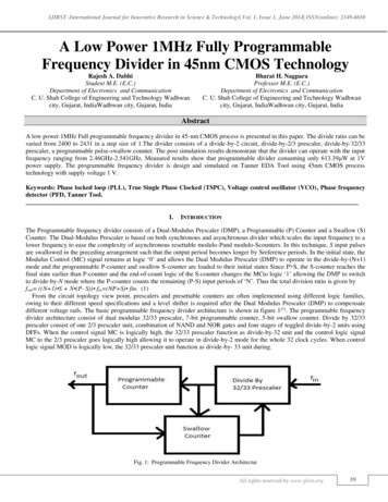
IJIRST–International Journal for Innovative Research in Science & Technology Vol. 1, Issue 1, June 2014 ISSN(online): 2349-6010A Low Power 1MHz Fully ProgrammableFrequency Divider in 45nm CMOS TechnologyRajesh A. DabhiStudent M.E. (E.C.)Department of Electronics and CommunicationC. U. Shah College of Engineering and Technology Wadhwancity, Gujarat, IndiaWadhwan city, Gujarat, IndiaBharat H. NagparaProfessor M.E. (E.C.)Department of Electronics and CommunicationC. U. Shah College of Engineering and Technology Wadhwancity, Gujarat, IndiaWadhwan city, Gujarat, IndiaAbstractA low power 1MHz Full programmable frequency divider in 45-nm CMOS process is presented in this paper. The divide ratio can bevaried from 2400 to 2431 in a step size of 1.The divider consists of a divide-by-2 circuit, divide-by-2/3 prescaler, divide-by-32/33prescaler, a programmable pulse-swallow counter. The post simulation results demonstrate that the divider can operate with the inputfrequency ranging from 2.46GHz-2.541GHz. Measured results show that programmable divider consuming only 613.39μW at 1Vpower supply. The programmable frequency divider is design and simulated on Tanner EDA Tool using 45nm CMOS processtechnology with supply voltage 1 V.Keywords: Phase locked loop (PLL), True Single Phase Clocked (TSPC), Voltage control oscillator (VCO), Phase frequencydetector (PFD, Tanner Tool.I.INTRODUCTIONThe Programmable frequency divider consists of a Dual-Modulus Prescaler (DMP), a Programmable (P) Counter and a Swallow (S)Counter. The Dual-Modulus Prescaler is based on both synchronous and asynchronous divider which scales the input frequency to alower frequency to ease the complexity of asynchronous resettable modulo-Pand modulo-Scounters. In this technique, S input pulsesare swallowed in the preceding arrangement such that the output period becomes longer by Sreference periods. In the initial state, theModulus Control (MC) signal remains at logic ‘0’ and allows the Dual Modulus Prescaler (DMP) to operate in the divide-by-(N 1)mode and the programmable P-counter and swallow S-counter are loaded to their initial states Since P S, the S-counter reaches thefinal state earlier than P-counter and the end-of-count logic of the S-counter changes the MCto logic ‘1’ allowing the DMP to switchto divide-by-N mode where the P-counter counts the remaining (P-S) input periods of ‘N’. Thus the total division ratio is given byfout ((N 1) S N (P- S)) fin (NP S) fin. (1)From the circuit topology view point, prescalers and presettable counters are often implemented using different logic families,owing to their different speed specifications and a level shifter is required after the Dual Modulus Prescaler (DMP) to compensatedifferent voltage rails. The basic programmable frequency divider architecture is shown in figure 1 [1]. The programmable frequencydivider architecture consist of dual modulus 32/33 prescaler, 7-bit programmable counter, 5-bit swallow counter. Divide by 32/33prescaler consist of one 2/3 prescaler unit, combination of NAND and NOR gates and four stages of toggled divide-by-2 units usingDFFs. When the control signal MC is logically high, the 32/33 prescaler function as divide-by-32 unit and the control logic signalMC to the 2/3 prescaler goes logically high allowing it to operate in divide-by-2 mode for the whole 32 clock cycles. When controllogic signal MOD is logically low, the 32/33 prescaler unit function as divide-by- 33 unit during.Fig. 1: Programmable Frequency Divider ArchitecturAll rights reserved by www.ijirst.org39
A Low Power 1MHz Fully Programmable Frequency Divider in 45nm CMOS Technology(IJIRST/ Volume 01 / Issue 01 / 007)II. DIVIDE BY 32/33 PRESCALERA.Divide By 32/33 PrescalerFigure 2 shows the topology of a general 32/33 prescaler [2]. When the control signal MC is logically high, the 32/33 prescalerfunction as divide-by-32 unit and the control logic signal MC to the 2/3 prescaler goes logically high allowing it to operate in divideby-2 mode for the whole 32 clock cycles. When control logic signal MC is logically low, the 32/33 prescaler unit function as divideby- 33 unit during which 2/3 prescaler operates in divide-by-3 mode for 3 input clock cycles and in divide-by-2 mode for 30 inputclock cycles [2].Fig. 2: Divide By 32/33 Prescaler1) Divide-By-32 operation (MOD ‘1’)When the control signal MOD is ‘1’, the output of NOR2 always remains at logic ‘0’ and forces the output of NAND2 to logic ‘1’irrespective of data on Qb1. Since MC is always equal to logic ‘1’, the Design of prescaler remains in divide-by-2. Thus the 32/33prescaler acts as divide-by-32 circuit. Since control logic signal MC is logically high, DFF1 in the 2/3 prescaler is completely turnedoff for the entire 32 input clock cycles. The 32/33 prescaler consists of both the synchronous and asynchronous (toggle divide-by-2)circuits and thus the power and speed is traded-off as discussed in the design of digital counters earlier. If we denote the synchronous2/3 prescaler as M/M 1 and the four asynchronous dividers whose division ratio equal to 16 by ‘AD’, the division ratio in this mode(MOD ‘1’) is given byf32 (AD-MOD) M MOD (M 1) 32 (2)2) Divide-By-33 operation (MOD ‘0’)The dual-modulus 32/33 prescaler operates as divide-by-33 when MOD ’0’. By using the combination of logic NOR and NANDgates, the asynchronous divide-by-16 counter is made to count an extra input clock. The control signal MC is given byMC Qb4 Qb3 Qb2 Qb1 MODIn the initial state, 2/3 prescaler will be in divide-by-2 mode (MC ‘1’) and the asynchronous divide-by16 starts counting the outputpulses of 2/3 prescaler from “0000” to “1111”. When the asynchronous counter value reaches “1110”, the logic signal MC goes low(MC ’0’) and the prescaler operates in divide-by-3 mode, where the asynchronous counter counts an extra input clock pulse. Duringthis operation, the 2/3 prescaler operates in divide-by-2 mode for 30 input clock cycles and for the remaining 3 input clock cycles; itoperates in divide-by-3 mode. The division of the 32/33 prescaler in this mode is given byf32 (AD-MOD) M MOD (M 1) 33 (3)where AD 16, MOD ’0’ and M ’2’.B. Divide By 2/3 PrescalerThe TSPC divide-by-2 unit has the merit of high operating frequency compared with the traditional TSPC divide-by 2 unit. Since thedivide-by-2/3 unit consists of two toggle DFFs and additional logic gates, one way to effectively reduce the delay and powerconsumption is to integrate the logic gates to the divide-by-2/3 unit [2]. Divide-by-2/3 counter design is given in Figure 3 consists oftwo TSPC-based FFs and two logic gates, an OR gate and an AND gate. When the divide control signal is low, the OR gate (mergedinto output of FF1 stage) is disabled. This corresponds to a divide-by-3 function. Note that state 10 is a forbidden state. If, somehow,the circuit enters this state, the next state will go back to a valid state, 11, automatically. When high is the output of FF1 will bedisabled and FF2 alone performs divide-by-2 function .The control logic signal MC selects the divide-by-2 or divide-by-3 mode.When MC is logically high DFF1 will disconnected from the power supply and DFF2 alone work to form the divide-by-2 operation.When the control signal MC goes low than both flip-flops combine give the divide-by-3 operation. Operating frequency is directlyrelated to the supply voltage.All rights reserved by www.ijirst.org40
A Low Power 1MHz Fully Programmable Frequency Divider in 45nm CMOS Technology(IJIRST/ Volume 01 / Issue 01 / 007)Fig. 3: Divide By 2/3 PrescalerThe Divide by 2/3 prescaler is implemented with True Signal Phase Clock (TSPC)logic. When control logic signal ‘MC’ goes high,the output of OR gate is always equal to logic ‘1’ and the output of AND gate is always equal to the inverted output of DFF2 (Q2)such that the prescaler operates in the divide-by-2 mode as shown in Fig. 3. When control logic signal ‘MC’ goes low, the output ofOR gate is always equal to ‘Q1’, such that prescaler operates in the divide-by-3 mode as shown in Figure 3. The output of thesynchronous 2/3 prescaler is given byfout MC ( fin /3) MC ( fin /2) (4)C. Divide By 2 CircuitThe divide by 2 circuit is realized in the TSPC logic as shown in figure 4 [5]. The salient feature of the TSPC clocking technique isthat there only one clock signal needed to trigger the flip-flop and no extra clock phase is required. This technique is mainly used indynamic CMOS circuits and helps to simplify the design. The circuit consists of three parts. The first part is gated inverter thatconsists of Mp1, Mp2, and Mn1, which passes the divider output to the following stage when the clock is low. The second part islatch stage that consists of Mp2, Mp3, Mn2, Mn3, Mn4, and Mn5. This circuit will be activated and store the output of the gateinverter when clock is high. The PMOS transistor Mp1 and Mp2 are used to pre-charge the internal nodes to increase the speed of thecircuit.The output of the flip-flop is directly connected back to the D-input to obtain the divided by 2 function because the TSPC circuitcan complicity isolated the sense and latch stage at different phase of the clock signal. The static power of the circuit is zero becausepath from the supply to ground exist and it only consumes dynamic power.Fig. 4: Divide By 2 circuit using TSPC logiD. Simulation Result of Divide By 2 CircuitThe transient analysis of divide by 2 circuit is shown in figure 5. The CLK frequency is 2.4GHz and Q is the divide by 2 outp utfrequency which is 1.2GHz.All rights reserved by www.ijirst.org41
A Low Power 1MHz Fully Programmable Frequency Divider in 45nm CMOS Technology(IJIRST/ Volume 01 / Issue 01 / 007)Fig. 5: Divided By 2 outputE. Simulation Result of 2/3 PrescalerThe figure 6 and 7 shows the transient analysis of the 2/3 prescaler respectively. The input CLK frequency is 2.4 GHz.When MC 1 its output is divided by 2, which is 1.2GHz and power dissipation is 59.15µW during divide by 2 operation. The figure6 divide by 2 operation.Fig. 6: Divided By 2 output of PrescalerWhen MC 0 its output is divided by 3, which is 801.28MHz and power dissipation is 61.47µW during divide by 2 operation. Thefigure 7 divide by 3 operation.Fig. 7: Divided By 3 output of PrescaleF. Simulation Result of 32/33 PrescalerThe figure 8 and 9 shows the transient analysis of the 32/33 prescaler respectively.The input CLK frequency is 2.4Ghz.When MC 1 its output is divided by 32, which is 75.11MHz and power dissipation is 85.62µWduring divide by 32 operation.All rights reserved by www.ijirst.org42
A Low Power 1MHz Fully Programmable Frequency Divider in 45nm CMOS Technology(IJIRST/ Volume 01 / Issue 01 / 007)Fig. 8: Divided By 32 output of PrescalerWhen MC 0 its output is divided by 33, which is 72.72MHz and power dissipation is 86.49µW during divide by 33 operation.Fig. 9: Divided By 33 output of PrescalerIII. P-S COUNTERFor PLL Frequency Synthesizers operating in the 2.4 GHz ISM band [4]-[3], with a resolution of 1MHz and division ratios of 24002484 can be achieved with a 32/33 prescaler, a 7 bit P-counter and a 5 bit S-counter.Fig.1 shows the fully programmable divider witha division ratio from 2400 to 2484 in steps of 1. In this design, only bits P1, P2 and P3 of the P-counter are used programming andthe bits P4, P5, P6 and P7 are fixed at ‘1’, ‘0’, ‘0’ and ‘1’ respectively to have P-values between 74-77. Here all the bits of S-counterare used for programming. The P and S counter’s programmable value for the division ratios between 2400-2484 is shown in Table6.1. This chapter briefly discusses the design of a fully programmable 1MHz resolution divider based on pulse swallow dividertopology.The Frequency Division ratio (FD) of the multi-band divider in this mode is given byFD N P – S(5)Where FD frequency division ratio, N Modulus value, P P-Counter value, S S-Counter value.Hence from table 1 it can be seen than the by changing the programming values of the Programmable P-Counter and SwallowCounter different frequency division ratio is achieved for frequency synthesizer.Table. 1: Programmable values of the Programmable CountersFrequencydivision ratioPrescaler (N/N 1)2400-2431N 32Programmablecounter (P)P 75Swallow counter(S)S 0-31All rights reserved by www.ijirst.org43
A Low Power 1MHz Fully Programmable Frequency Divider in 45nm CMOS Technology(IJIRST/ Volume 01 / Issue 01 / 007)2432-2463N 32P 762464-2484N 32P 77S 0-31S 0-20A. Programmable CounterThe 32/33 prescaler scales the input 2.4 GHz signal by a value of 32 or 33 such that the P and S counters will be working in thefrequency range of 72 - 78 MHz in order to obtain the 1 MHz frequency output. The design requirements of the P-counter in thedesign of 2.4 GHz fully programmable divider are as follows: Operate at frequencies of up to several 100 MHz with low power consumption. Able to program the desired P values from 74 to 77. To generate full-swing output, which is fed to the phase frequency detector blockFig. 10: A 7-bit programmable P-CounterThe Programmable P-Counter used in the design of the fully programmable divider is a 7-bit asynchronous down counter as shownin Fig.10[4]. The P-counter is designed with 7 reloadable TSPC D Flip-Flops (DFF) and an End-Of- Count (EOC) detector which hasreload circuit in it [3]. Since the counter is asynchronous and based on the ring topology, the complementary output of the first DFF isfed as clock to the input of next flip-flop. In the initial state, all the reloadable FF’s are loaded by the programmable pins P1-P7. Asthe counter is triggered by the output of the prescaler, the P-counter starts down counting till the state “0000000” is reached. Oncethis state is detected by the EOC logic circuit, the load (LD) signal goes high to reset all loadable FF’s to the initial state.B. Swallow S-CounterThe fully programmable divider also consists of a 5-bit swallow S-Counter whose design requirements are as follows: To operate at frequencies of up to several 100 MHz with low power consumption. To load the programmable S values from 0 to 31 in steps of one and stop the operation when S counting is finished. To generate a full-swing output, this is given as feedback signal to phase frequency detector blockFigure. 11 A 5-bit Swallow S-CounterAll rights reserved by www.ijirst.org44
A Low Power 1MHz Fully Programmable Frequency Divider in 45nm CMOS Technology(IJIRST/ Volume 01 / Issue 01 / 007)The Swallow S-Counter used in the design of the fully programmable divider is a 5-bit asynchronous down counter as shown inFig.11. The S-counter is designed with 5 reloadable TSPC D flip-flops and an End-Of- Count (EOC) detector with the reload circuit[1]. Since the counter is asynchronous and based on the ring topology, the complementary output of the first DFF is fed as clock to theinput of next flip-flop. In the initial state, all the reloadable FF’s are loaded by the programmable value set by pins S1-S5. In the Scounter all states from 0-31 are usable and adjustable in steps of 1 to obtain a resolution of 1MHz. Once the counter is triggered bythe output of the prescaler, the S-counter starts down counting till the final state is reached, which is detected by the EOC logiccircuit and the stop (SP) signal goes high until the P-counter finishes it’s counting. Since the value of ‘P’ is always greater than valueof ‘S’ in pulse-swallow divider, the S-counter remains idle for a period of (P-S)*N clock cycles.IV. SIMULATION RESULT OF PROGRAMMABLE FREQUENCY DIVIDERThe simulations of the fully Programmable Frequency Divider with 1MHz resolution are performed using Tanner EDA tool for a 45nm CMOS process. Fig.13 shows the simulation results of the fully programmable divider. The simulations are performed by givinga 2.4GHz square wave signal with amplitude of 0.5V (peak) to the prescaler. Here the programmability of the divider is set to 2400and the results indicate that the output of the fully programmable divider is 1MHz.Figure 12 shows Schematic view of ProgrammableFrequency Divider.Fig. 12: Schematic view of Programmable Frequency DividerFigure 13 Simulation Result of Programmable Frequency DividerTable. 2:. Frequency Divider Performance SummarySpecificationTechnologySupply voltageFrequency BandRef. Frequency2 Prescaler3 PrescalerPower Dissipation32 Prescaler33 PrescalerFrequency DividerSimulation 5.62µW/86.42µW613.39µWAll rights reserved by www.ijirst.org45
A Low Power 1MHz Fully Programmable Frequency Divider in 45nm CMOS Technology(IJIRST/ Volume 01 / Issue 01 / 007)V. CONCLUSIONThis paper presents a programmable frequency divider designed in 45-nm CMOS process with divide ratio varied from 2400 to 2431in a step of 1. The post simulation results show that the divider can work properly with the input frequency from 2.44GHz to 2.54GHz while the power consumption is 613.39µW at supply voltage of 1V. The DFF in the prescaler is controlled by the modecontrolling signal and powered off in the idle state, the DFFs in the program counter and swallow counter are shared, and thus powerconsumption is reduced. The experimental results show large power reduction is achieved by the proposed divider. We can concludethat the proposed divider is well suitable for low power design.REFERENCE[1][2][3][4][5]Haijun Gao, Lingling Sun and Jun Liu. “Pulse swallow frequency divider with idle DFFs automatically powered off”. ELECTRONICS LETTERS 24 th May2012 Vol. 48 No.11.Don P John, “High Frequency 32/33 Prescalers Using 2/3 Prescaler Technique”. IJER, Jul-Aug 2013, pp.655-661.ISSN: 2248-9622, Vol. 3, Issue 4.Vamshi Krishna Manthena,Manh Anh Do,Chirn Chye Boon, and Kiat Seng Yeo. “ A Low-Power Single-Phase Clock Multiband Flexible Divider”. IEEEtransactions on VLSI system, February 2012, pp.376-380 vol. 20, no. 2.Razavi Behzad, Principles of Data Conversion System Design, IEEE Press, 1995.R. Jacob Baker, CMOS Circuit Design, Layout and Simulation, Third Edition, Wiley Publication, 1964, pp. 1-31, 931-1022.All rights reserved by www.ijirst.org46
A low power 1MHz Full programmable frequency divider in 45-nm CMOS process is presented in this paper. The divide ratio can be varied from 2400 to 2431 in a step size of 1.The divider consists of a divide-by-2 circuit, divide-by-2/3 prescaler, divide-by-32/33 prescaler, a programmable pulse-swallow counter.
