Transcription
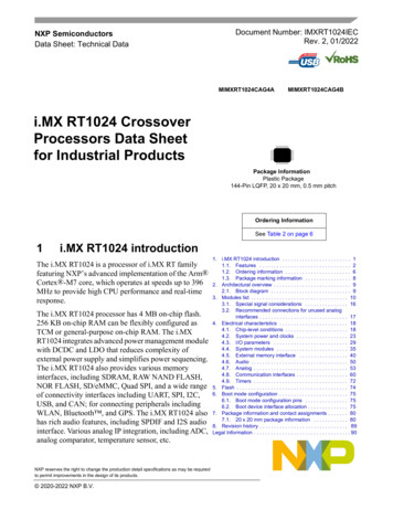
NXP SemiconductorsData Sheet: Technical DataDocument Number: IMXRT1024IECRev. 2, 01/2022MIMXRT1024CAG4AMIMXRT1024CAG4Bi.MX RT1024 CrossoverProcessors Data Sheetfor Industrial ProductsPackage InformationPlastic Package144-Pin LQFP, 20 x 20 mm, 0.5 mm pitchOrdering InformationSee Table 2 on page 61i.MX RT1024 introductionThe i.MX RT1024 is a processor of i.MX RT familyfeaturing NXP’s advanced implementation of the Arm Cortex -M7 core, which operates at speeds up to 396MHz to provide high CPU performance and real-timeresponse.The i.MX RT1024 processor has 4 MB on-chip flash.256 KB on-chip RAM can be flexibly configured asTCM or general-purpose on-chip RAM. The i.MXRT1024 integrates advanced power management modulewith DCDC and LDO that reduces complexity ofexternal power supply and simplifies power sequencing.The i.MX RT1024 also provides various memoryinterfaces, including SDRAM, RAW NAND FLASH,NOR FLASH, SD/eMMC, Quad SPI, and a wide rangeof connectivity interfaces including UART, SPI, I2C,USB, and CAN; for connecting peripherals includingWLAN, Bluetooth , and GPS. The i.MX RT1024 alsohas rich audio features, including SPDIF and I2S audiointerface. Various analog IP integration, including ADC,analog comparator, temperature sensor, etc.NXP reserves the right to change the production detail specifications as may be requiredto permit improvements in the design of its products. 2020-2022 NXP B.V.1. i.MX RT1024 introduction . . . . . . . . . . . . . . . . . . . . . . . . 11.1. Features . . . . . . . . . . . . . . . . . . . . . . . . . . . . . . . . 21.2. Ordering information . . . . . . . . . . . . . . . . . . . . . . . 61.3. Package marking information . . . . . . . . . . . . . . . . 82. Architectural overview . . . . . . . . . . . . . . . . . . . . . . . . . . . 92.1. Block diagram . . . . . . . . . . . . . . . . . . . . . . . . . . . . 93. Modules list . . . . . . . . . . . . . . . . . . . . . . . . . . . . . . . . . . 103.1. Special signal considerations . . . . . . . . . . . . . . . 163.2. Recommended connections for unused analoginterfaces . . . . . . . . . . . . . . . . . . . . . . . . . . . . . . . 174. Electrical characteristics . . . . . . . . . . . . . . . . . . . . . . . . 184.1. Chip-level conditions . . . . . . . . . . . . . . . . . . . . . . 184.2. System power and clocks . . . . . . . . . . . . . . . . . . 234.3. I/O parameters . . . . . . . . . . . . . . . . . . . . . . . . . . 294.4. System modules . . . . . . . . . . . . . . . . . . . . . . . . . 354.5. External memory interface . . . . . . . . . . . . . . . . . 404.6. Audio . . . . . . . . . . . . . . . . . . . . . . . . . . . . . . . . . . 504.7. Analog . . . . . . . . . . . . . . . . . . . . . . . . . . . . . . . . . 534.8. Communication interfaces . . . . . . . . . . . . . . . . . . 604.9. Timers . . . . . . . . . . . . . . . . . . . . . . . . . . . . . . . . . 725. Flash . . . . . . . . . . . . . . . . . . . . . . . . . . . . . . . . . . . . . . . 746. Boot mode configuration . . . . . . . . . . . . . . . . . . . . . . . . 756.1. Boot mode configuration pins . . . . . . . . . . . . . . . 756.2. Boot device interface allocation . . . . . . . . . . . . . . 757. Package information and contact assignments . . . . . . . 807.1. 20 x 20 mm package information . . . . . . . . . . . . 808. Revision history . . . . . . . . . . . . . . . . . . . . . . . . . . . . . . . 89Legal Information . . . . . . . . . . . . . . . . . . . . . . . . . . . . . . . . . . 90
i.MX RT1024 introductionThe i.MX RT1024 is specifically useful for applications such as: Industrial Motor Control Home Appliance IoT1.1FeaturesThe i.MX RT1024 processors are based on Arm Cortex-M7 Core Platform, which has the followingfeatures: Supports single Arm Cortex-M7 with:— 16 KB L1 Instruction Cache— 16 KB L1 Data Cache— Full featured Floating Point Unit (FPU) with support of the VFPv5 architecture— Support the Armv7-M Thumb instruction set Integrated MPU, up to 16 individual protection regions Up to 256 KB I-TCM and D-TCM in total Frequency of 396 MHz Cortex M7 CoreSight components integration for debug Frequency of the core, as per Table 11, "Operating ranges," on page 19.The SoC-level memory system consists of the following additional components:— Boot ROM (96 KB)— On-chip Flash (4 MB)— On-chip RAM (256 KB)– Configurable RAM size up to 256 KB shared with CM7 TCM External memory interfaces:— 8/16-bit SDRAM, up to SDRAM-133— 8/16-bit SLC NAND FLASH, with ECC handled in software— SD/eMMC— SPI NOR/NAND FLASH— Parallel NOR FLASH with XIP support— Single/Dual channel Quad SPI FLASH with XIP support Timers and PWMs:— Two General Programmable Timers– 4-channel generic 32-bit resolution timer– Each support standard capture and compare operation— Four Periodical Interrupt Timers– Generic 32-bit resolution timeri.MX RT1024 Crossover Processors Data Sheet for Industrial Products, Rev. 2, 01/20222NXP Semiconductors
i.MX RT1024 introduction– Periodical interrupt generation— Two Quad Timers– 4-channel generic 16-bit resolution timer each– Each support standard capture and compare operation– Quadrature decoder integrated— Two FlexPWMs– Up to 8 individual PWM channels per each– 16-bit resolution PWM suitable for Motor Control applications— Two Quadrature Encoders/DecodersEach i.MX RT1024 processor enables the following interfaces to external devices (some of them aremultiplexed and not available simultaneously): Audio:— S/PDIF input and output— Three synchronous audio interface (SAI) modules supporting I2S, AC97, TDM, andcodec/DSP interfaces— MQS interface for medium quality audio via GPIO pads Connectivity:— One USB 2.0 OTG controller with integrated PHY interface— Two Ultra Secure Digital Host Controller (uSDHC) interfaces– MMC 4.5 compliance support up to 100 MB/sec– SD/SDIO 3.0 compliance with 200 MHz SDR signaling to support up to 100 MB/sec– Support for SDXC (extended capacity)— One 10M/100M Ethernet controller with IEEE1588 supported— Eight universal asynchronous receiver/transmitter (UARTs) modules— Four I2C modules— Four SPI modules— Two FlexCAN modules GPIO and Pin Multiplexing:— General-purpose input/output (GPIO) modules with interrupt capability— Input/output multiplexing controller (IOMUXC) to provide centralized pad control— 90 GPIOs for 144-pin LQFP package— One FlexIOThe i.MX RT1024 processors integrate Analog module:— Two Analog-Digital-Converters (ADC), up to 19 channels— Four Analog Comparators (ACMP)The i.MX RT1024 processors integrate advanced power management unit and controllers: Full PMIC integration, including on-chip DCDC and LDOsi.MX RT1024 Crossover Processors Data Sheet for Industrial Products, Rev. 2, 01/2022NXP Semiconductors3
i.MX RT1024 introduction Temperature sensor with programmable trip pointsGPC hardware power management controllerThe i.MX RT1024 processors support the following system debug: Arm CortexM7 CoreSight debug and trace architecture Trace Port Interface Unit (TPIU) to support off-chip real-time trace Support for 5-pin (JTAG) and SWD debug interfaces selected by eFuseSecurity functions are enabled and accelerated by the following hardware: High Assurance Boot (HAB) Data Co-Processor (DCP):— AES-128, ECB, and CBC mode— SHA-1 and SHA-256— CRC-32 Bus Encryption Engine (BEE)— AES-128, ECB, and CTR mode— On-the-fly QSPI Flash decryption True random number generation (TRNG) Secure Non-Volatile Storage (SNVS)— Secure real-time clock (RTC)— Zero Master Key (ZMK) Secure JTAG Controller (SJC)NOTEThe actual feature set depends on the part numbers as described in Table 2.Functions such as display and camera interfaces, connectivity interfaces,and security features are not offered on all derivatives.i.MX RT1024 Crossover Processors Data Sheet for Industrial Products, Rev. 2, 01/20224NXP Semiconductors
i.MX RT1024 introductionTable 1 lists the comparison between RT1020 and RT1024.Table 1. The comparison between RT1020 and RT1024RT1020RT1024Package144 LQFP144 LQFPFrequency500 MHz, Consumer grade396 MHz, Industrial grade500 MHz, Consumer grade396 MHz, Industrial gradeRAM256 KB256 KBFlashNA4 MBCAN22Ethernet111588 EVENT42eMMC4.5/SD3.022USB PI44ADC22ACMP44GPIO9690i.MX RT1024 Crossover Processors Data Sheet for Industrial Products, Rev. 2, 01/2022NXP Semiconductors5
i.MX RT1024 introduction1.2Ordering informationTable 2 provides examples of orderable part numbers covered by this data sheet.Table 2. Ordering informationPart NumberFeaturePackageJunctionTemperature Tj ( C)MIMXRT1024CAG4A 396 MHz, industrial grade for generalpurpose 256K RAM 4MB flash CAN x2 Ethernet eMMC 4.5/SD 3.0 x2 USB OTG x1 SAI x3 SPDIF x1 Timer x2 PWM x2 UART x8 I2C x4 SPI x4 ADC x2 ACMP x4 90 GPIOs20 x 20 mm, 0.5 mm pitch,144-pin LQFP-40 to 105MIMXRT1024CAG4B 396 MHz, industrial grade for generalpurpose 256K RAM 4MB flash CAN x2 Ethernet eMMC 4.5/SD 3.0 x2 USB OTG x1 SAI x3 SPDIF x1 Timer x2 PWM x2 UART x8 I2C x4 SPI x4 ADC x2 ACMP x4 90 GPIOs20 x 20 mm, 0.5 mm pitch,144-pin LQFP-40 to 105Figure 1 describes the part number nomenclature so that characteristics of a specific part number can beidentified (for example, cores, frequency, temperature grade, fuse options, and silicon revision). Theprimary characteristic which describes which data sheet applies to a specific part is the temperature grade(junction) field.Ensure to have the proper data sheet for specific part by verifying the temperature grade (junction) fieldand matching it to the proper data sheet. If there are any questions, visit the web page nxp.com/IMXRT orcontact an NXP representative for details.i.MX RT1024 Crossover Processors Data Sheet for Industrial Products, Rev. 2, 01/20226NXP Semiconductors
i.MX RT1024 introductionMIMXXX@##% VV AQualification LevelMSilicon RevAPrototype SamplesPA0AMass ProductionMA1BSpecialSCore Frequency 400 MHz4500 MHz5600 MHz6Part # seriesXXi.MX RTRTFamily@First Generation RT family1ReservedPackage Type2-8VV225MAPBGA, 13 x 13 mm, 0.8 mm pitchVNSub-Family##196MAPBGA, 12 x 12 mm, 0.8 mm pitchVJRT101x01196MAPBGA, 10 x 10 mm, 0.65 mm pitchVLRT102x02169MAPBGA, 11 x 11 mm, 0.8 mm pitchJMRT104x04169MAPBGA, 9 x 9 mm, 0.65 mm pitchFPRT105x05144LQFP, 20 x 20 mm, 0.5 mm pitchAGRT106x06Tie%Standard Feature1Full Feature24MB Flash SIP4100LQFP, 14 x 14 mm, 0.5 mm pitchAF80LQFP, 12 x 12 mm, 0.5 mm pitchAEEnhanced Feature5Temperature (Tj) Far Field AFEAConsumer: 0 to 95 CDFacial RecognitionFIndustrial: -40 to 105 CCLocal Voice Control (audio input models)LExtended Industrial: -40 to 125 eCXLocal Voice Control (text input models)SFigure 1. Part number nomenclature—i.MX RT10XX familyi.MX RT1024 Crossover Processors Data Sheet for Industrial Products, Rev. 2, 01/2022NXP Semiconductors7
i.MX RT1024 introduction1.3Package marking informationFigure 2 describes the package marking format about the i.MX RT1024 Crossover Processors.Figure 2. Package marking formatThe i.MX RT1024 package has the following top-side marking: First line: aaaaaaaaaaaaaaa Second line: mmmmm Third line: xxxyywwxTable 3 lists the identifier decoder.Table 3. Identifier decoderIdentifierDescriptionaPart number code, refer to Section 1.2, Ordering informationmMask setyYearwWork weekxNXP internal usei.MX RT1024 Crossover Processors Data Sheet for Industrial Products, Rev. 2, 01/20228NXP Semiconductors
Architectural overview2Architectural overviewThe following subsections provide an architectural overview of the i.MX RT1024 processor system.2.1Block diagramFigure 3 shows the functional modules in the i.MX RT1024 processor system1.System ControlMain CPU PlatformDCDC and LDOCore2 x CAN5 x 5 KeypadeDMAArm Cortex -M710/100 ENETwith IEEE 1588S/PDIF Tx/RxIOMUX16 KB I-cacheConnectivity16 KB D-cache4 x SPI2 x eMMC 4.5/SD 3.0PLL, OSC2 x Quadrature ENCFPUMPUNVIC8 x UARTGPIOUp to 256 KB TCMUSB 2.0 OTGw/ PHY24xICSecure JTAGExternal MemoryTemp MonitorDual-Channel QSPI FLASHwith Bus Encryption Engine3 x I2SInternal Memory256 KB SRAM/TCM4 MB FlashExternal Memory Controller8/16-bit SDRAMParallel NOR FlashNAND FlashTimers2 x GP Timer2 x QuadTimer2 x FlexPWM4 x WatchdogAnalog2 x ADC96 KB ROM4 x Analog ComparatorSecurityCiphers and RNGeFuseHABSecure RTC.Figure 3. i.MX RT1024 system block diagram1. Some modules shown in this block diagram are not offered on all derivatives. See Table 2 for details.i.MX RT1024 Crossover Processors Data Sheet for Industrial Products, Rev. 2, 01/2022NXP Semiconductors9
Modules list3Modules listThe i.MX RT1024 processors contain a variety of digital and analog modules. Table 4 describes thesemodules in alphabetical order.Table 4. i.MX RT1024 modules listBlock mnemonicBlock nameSubsystemBrief descriptionACMP1ACMP2ACMP3ACMP4Analog ComparatorAnalogThe comparator (CMP) provides a circuit for comparingtwo analog input voltages. The comparator circuit isdesigned to operate across the full range of the supplyvoltage (rail-to-rail operation).ADC1ADC2Analog to DigitalConverterAnalogThe ADC is a 12-bit general purpose analog to digitalconverter.AOIAnd-Or-InverterCross TriggerThe AOI provides a universal boolean functiongenerator using a four team sum of products expressionwith each product term containing true or complementvalues of the four selected inputs (A, B, C, D).ArmArm PlatformArmThe Arm Core Platform includes 1x Cortex-M7 core. Italso includes associated sub-blocks, such as NestedVectored Interrupt Controller (NVIC), Floating-PointUnit (FPU), Memory Protection Unit (MPU), andCoreSight debug modules.BEEBus Encryption EngineSecurityOn-The-Fly FlexSPI Flash DecryptionCCMGPCSRCClocks, Resets, and These modules are responsible for clock and resetClock Control Module,Power Controldistribution in the system, and also for the systemGeneral Powerpower management.Controller, System ResetControllerCSUCentral Security UnitSecurityThe Central Security Unit (CSU) is responsible forsetting comprehensive security policy within the i.MXRT1024 platform.DAPDebug Access PortSystem ControlPeripheralsThe DAP provides real-time access for the debuggerwithout halting the core to: System memory and peripheral registers All debug configuration registersThe DAP also provides debugger access to JTAG scanchains. The DAP module is internal to the Cortex-M7Core Platform.DCDCDCDC ConverterAnalogThe DCDC module is used for generating power supplyfor core logic. Main features are: Adjustable high efficiency regulator Supports 3.3 V input voltage Supports nominal run and low power standby modes Supports at 0.9 1.3 V output in run mode Supports at 0.9 1.0 V output in standby mode Over current and over voltage detectioni.MX RT1024 Crossover Processors Data Sheet for Industrial Products, Rev. 2, 01/202210NXP Semiconductors
Modules listTable 4. i.MX RT1024 modules list (continued)Block mnemonicBlock nameSubsystemBrief descriptioneDMAenhanced Direct Memory System ControlAccessPeripheralsThere is an enhanced DMA (eDMA) engine and twoDMA MUX. The eDMA is a 32 channel DMA engine, which iscapable of performing complex data transfers withminimal intervention from a host processor. The DMA MUX is capable of multiplexing up to 128DMA request sources to the 32 DMA channels ofeDMA.ENCQuadratureEncoder/DecoderTimer PeripheralsThe enhanced quadrature encoder/decoder moduleprovides interfacing capability to position/speedsensors. There are five input signals: PHASEA,PHASEB, INDEX, TRIGGER, and HOME. This moduleis used to decode shaft position, revolution count, andspeed.ENETEthernet ControllerConnectivityPeripheralsThe Ethernet Media Access Controller (MAC) isdesigned to support 10/100 Mbit/s Ethernet/IEEE 802.3networks. An external transceiver interface andtransceiver function are required to complete theinterface to the media. The module has dedicatedhardware to support the IEEE 1588 standard. See theENET chapter of the reference manual for details.EWMExternal WatchdogMonitorTimer PeripheralsThe EWM modules is designed to monitor externalcircuits, as well as the software flow. This provides aback-up mechanism to the internal WDOG that canreset the system. The EWM differs from the internalWDOG in that it does not reset the system. The EWM,if allowed to time-out, provides an independent triggerpin that when asserted resets or places an externalcircuit into a safe mode.FLEXCAN1FLEXCAN2Flexible Controller AreaNetworkConnectivityPeripheralsThe CAN protocol was primarily, but not only, designedto be used as a vehicle serial data bus, meeting thespecific requirements of this field: real-time processing,reliable operation in the Electromagnetic interference(EMI) environment of a vehicle, cost-effectiveness andrequired bandwidth. The FlexCAN module is a fullimplementation of the CAN protocol specification,Version 2.0 B, which supports both standard andextended message frames.FlexIO1Flexible Input/outputConnectivity andCommunicationsThe FlexIO is capable of supporting a wide range ofprotocols including, but not limited to: UART, I2C, SPI,I2S, camera interface, display interface, PWMwaveform generation, etc. The module can remainfunctional when the chip is in a low power modeprovided the clock it is using remain active.i.MX RT1024 Crossover Processors Data Sheet for Industrial Products, Rev. 2, 01/2022NXP Semiconductors11
Modules listTable 4. i.MX RT1024 modules list (continued)Block mnemonicBlock nameSubsystemBrief descriptionFlexPWM1FlexPWM2Pulse Width ModulationTimer PeripheralsThe pulse-width modulator (PWM) contains four PWMsub-modules, each of which is set up to control a singlehalf-bridge power stage. Fault channel support isprovided. The PWM module can generate variousswitching patterns, including highly sophisticatedwaveforms.FlexRAMRAMMemoriesThe i.MX RT1024 has 256 KB of on-chip RAM whichcould be flexible allocated to I-TCM, D-TCM, andon-chip RAM (OCRAM) in a 32 KB granularity. TheFlexRAM is the manager of the 256 KB on-chip RAMarray. Major functions of this blocks are: interfacing toI-TCM and D-TCM of Arm core and OCRAM controller;dynamic RAM arrays allocation for I-TCM, D-TCM, andOCRAM.FlexSPIQuad Serial PeripheralInterfaceConnectivity andCommunicationsFlexSPI acts as an interface to one or two externalserial flash devices, each with up to four bidirectionaldata lines.GPIO1GPIO2GPIO3GPIO5General Purpose I/OModulesSystem ControlPeripheralsUsed for general purpose input/output to external ICs.Each GPIO module supports up to 32 bits of I/O.GPT1GPT2General Purpose TimerTimer PeripheralsEach GPT is a 32-bit “free-running” or “set and forget”mode timer with programmable prescaler and compareand capture register. A timer counter value can becaptured using an external event and can be configuredto trigger a capture event on either the leading or trailingedges of an input pulse. When the timer is configured tooperate in “set and forget” mode, it is capable ofproviding precise interrupts at regular intervals withminimal processor intervention. The counter has outputcompare logic to provide the status and interrupt atcomparison. This timer can be configured to run eitheron an external clock or on an internal clock.KPPKeypad PortHuman MachineInterfacesThe KPP is a 16-bit peripheral that can be used as akeypad matrix interface or as general purposeinput/output (I/O). It supports 5 x 5 external key padmatrix. Main features are: Multiple-key detection Long key-press detection Standby key-press detection Supports a 2-point and 3-point contact key matrixLPI2C1LPI2C2LPI2C3LPI2C4Low PowerInter-integrated CircuitConnectivity andCommunicationsThe LPI2C is a low power Inter-Integrated Circuit (I2C)module that supports an efficient interface to an I2C busas a master.The I2C provides a method of communication betweena number of external devices. More detailedinformation, see Section 4.8.2, LPI2C module timingparameters.i.MX RT1024 Crossover Processors Data Sheet for Industrial Products, Rev. 2, 01/202212NXP Semiconductors
Modules listTable 4. i.MX RT1024 modules list (continued)Block mnemonicBlock nameSubsystemBrief descriptionLPSPI1LPSPI2LPSPI3LPSPI4Low Power SerialPeripheral InterfaceConnectivity andCommunicationsThe LPSPI is a low power Serial Peripheral Interface(SPI) module that support an efficient interface to anSPI bus as a master and/or a slave. It can continue operating while the chip is in stopmodes, if an appropriate clock is available Designed for low CPU overhead, with DMA offloading of FIFO register UART7LPUART8UART InterfaceConnectivityPeripheralsEach of the UART modules support the following serialdata transmit/receive protocols and configurations: 7- or 8-bit data words, 1 or 2 stop bits, programmableparity (even, odd or none) Programmable baud rates up to 20 Mbps.MQSMedium Quality SoundMultimediaPeripheralsMQS is used to generate 2-channel medium qualityPWM-like audio via two standard digital GPIO pins.QuadTimer1QuadTimer2QuadTimerTimer PeripheralsThe quad-timer provides four time channels with avariety of controls affecting both individual andmulti-channel features.Specific features includeup/down count, cascading of counters, programmablemodule, count once/repeated, counter preload,compare registers with preload, shared use of inputsignals, prescaler controls, independentcapture/compare, fault input control, programmableinput filters, and multi-channel synchronization.ROMCPROM Controller withPatchMemories andThe ROMCP acts as an interface between the ArmMemory Controllers advanced high-performance bus and the ROM. Theon-chip ROM is only used by the Cortex-M7 core duringboot up. Size of the ROM is 96 KB.RTC OSCReal Time ClockOscillatorClock Sources andControlThe RTC OSC provides the clock source for theReal-Time Clock module. The RTC OSC module, inconjunction with an external crystal, generates a 32.768kHz reference clock for the RTC.RTWDOGWatch DogTimer PeripheralsThe RTWDG module is a high reliability independenttimer that is available for system to use. It provides asafety feature to ensure software is executing asplanned and the CPU is not stuck in an infinite loop orexecuting unintended code. If the WDOG module is notserviced (refreshed) within a certain period, it resets theMCU. Windowed refresh mode is supported as well.SAI1SAI2SAI3Synchronous AudioInterfaceMultimediaPeripheralsThe SAI module provides a synchronous audiointerface (SAI) that supports full duplex serial interfaceswith frame synchronization, such as I2S, AC97, TDM,and codec/DSP interfaces.SA-TRNGStandalone True Random SecurityNumber GeneratorThe SA-TRNG is hardware accelerator that generatesa 512-bit entropy as needed by an entropy consumingmodule or by other post processing functions.i.MX RT1024 Crossover Processors Data Sheet for Industrial Products, Rev. 2, 01/2022NXP Semiconductors13
Modules listTable 4. i.MX RT1024 modules list (continued)Block mnemonicBlock nameSubsystemBrief descriptionSEMCSmart External MemoryControllerMemory andMemory ControllerThe SEMC is a multi-standard memory controlleroptimized for both high-performance and low pin-count.It can support multiple external memories in the sameapplication with shared address and data pins. Theinterface supported includes SDRAM, NOR Flash,SRAM, and NAND Flash, as well as 8080 displayinterface.SJCSystem JTAG ControllerSystem ControlPeripheralsThe SJC provides JTAG interface, which complies withJTAG TAP standards, to internal logic. The i.MXRT1024 processors use JTAG port for production,testing, and system debugging. In addition, the SJCprovides BSR (Boundary Scan Register) standardsupport, which complies with IEEE1149.1 andIEEE1149.6 standards.The JTAG port is accessible during platform initiallaboratory bring-up, for manufacturing tests andtroubleshooting, as well as for software debugging byauthorized entities. The i.MX RT1024 SJC incorporatesthree security modes for protecting againstunauthorized accesses. Modes are selected througheFUSE configuration.SNVSSecure Non-VolatileStorageSecuritySecure Non-Volatile Storage, including Secure RealTime Clock, Security State Machine, and Master KeyControl.SPDIFSony Philips DigitalInterconnect FormatMultimediaPeripheralsA standard audio file transfer format, developed jointlyby the Sony and Phillips corporations. Has Transmitterand Receiver functionality.Temp MonitorTemperature MonitorAnalogThe temperature sensor implements a temperaturesensor/conversion function based on atemperature-dependent voltage to time conversion.USBO2Universal Serial Bus 2.0ConnectivityPeripheralsUSBO2 (USB OTG1) contains: One high-speed OTG 2.0 module with integrated HSUSB PHY Support eight Transmit (TX) and eight Receive (Rx)endpoints, including endpoint 0i.MX RT1024 Crossover Processors Data Sheet for Industrial Products, Rev. 2, 01/202214NXP Semiconductors
Modules listTable 4. i.MX RT1024 modules list (continued)Block mnemonicBlock nameSubsystemBrief descriptionuSDHC1uSDHC2ConnectivitySD/MMC and SDXCPeripheralsEnhanced Multi-MediaCard / Secure Digital HostControlleri.MX RT1024 specific SoC characteristics:All four MMC/SD/SDIO controller IPs are identical andare based on the uSDHC IP. They are: Fully compliant with MMC command/response setsand Physical Layer as defined in the MultimediaCard System Specification, v4.5/4.2/4.3/4.4/4.41/including high-capacity (size 2 GB) cards HCMMC. Fully compliant with SD command/response setsand Physical Layer as defined in the SD MemoryCard Specifications, v3.0 including high-capacitySDXC cards up to 2 TB. Fully compliant with SDIO command/response setsand interrupt/read-wait mode as defined in the SDIOCard Specification, Part E1, v3.0Two ports support: 1-bit or 4-bit transfer mode specifications for SD andSDIO cards up to UHS-I SDR104 mode (104 MB/smax) 1-bit, 4-bit, or 8-bit transfer mode specifications forMMC cards up to 52 MHz in both SDR and DDRmodes (104 MB/s max) 4-bit transfer mode specifications for eMMC chips upto 100 MHz in HS200 mode (100 MB/s max)WDOG1WDOG2Watch DogTimer PeripheralsThe Watch Dog Timer supports two comparison pointsduring each counting period. Each of the comparisonpoints is configurable to evoke an interrupt to the Armcore, and a second point evokes an external event onthe WDOG line.XBARCross BARCross TriggerEach crossbar switch is an array of muxes with sharedinputs. Each mux output provides one output of thecrossbar. The number of inputs and the number ofmuxes/outputs are user configurable and registers areprovided to select which of the shared inputs are routedto each output.i.MX RT1024 Crossover Processors Data Sheet for Industrial Products, Rev. 2, 01/2022NXP Semiconductors15
Modules list3.1Special signal considerationsTable 5 lists special signal considerations for the i.MX RT1024 processors. The signal names are listed inalphabetical order.The package contact assignments can be found in Section 7, Package information and contactassignments.” Signal descriptions are provided in the i.MX RT1024 Reference Manual(IMXRT1024RM).Table 5. Special signal considerationsSignal nameRemarksDCDC PSWITCHPAD is in DCDC IN domain and connected the ground to bypass DCDC.To enable DCDC function, assert to DCDC IN with at least 1ms delay for DCDC IN rising edge.RTC XTALI/RTC XTALOIf the user wishes to configure RTC XTALI and RTC XTALO as an RTC oscillator, a 32.768 kHzcrystal, ( 100 k ESR, 10 pF load) should be connected between RTC XTALI and RTC XTALO.Keep in mind the capacitors implemented on either side of the crystal are about twice the crystalload capacitor. To hit the exact oscillation frequency, the board capacitors need to be reduced toaccount for board and chip parasitics. The integrated oscillation amplifier is self biasing, butrelatively weak. Care must be taken to limit parasitic leakage from RTC XTALI and RTC XTALOto either power or ground ( 100 M ). This will debias the amplifier and cause a reduction ofstartup margin. Typically RTC XTALI and RTC XTALO should bias to approximately 0.5 V.If it is desired to feed an external low frequency clock into RTC XTALI the RTC XTALO pin mustremain unconnected or driven with a complimentary signal. The logic level of this forcing clockshould not exceed VDD SNVS CAP level and the frequency should be 100 kHz under typicalconditions.In case when high accuracy real time clock are not required system may use internal lowfrequency ring oscillator. It is recommended to connect RTC XTALI to GND and keepRTC XTALO unconnected.XTALI/XTALOA 24.0 MHz crystal should be connected between XTALI and XTALO. External load capacitancevalue depends on the typical load capacitance of crystal used and PCB design.The crystal must be rated for a maximum drive level of 250 W. An ESR (equivalent seriesresistance) of typical 80 is recommended. NXP SDK software requires 24 MHz onXTALI/XTALO.The crystal can be eliminated if an external 24 MHz oscillator is available in the system. In thiscase, XTALO must be directly driven by the external oscillator and XTALI mounted with 18 pFcapacitor. The logic level of this forcing clock cannot exceed NVCC PLL level.If this clock is used as a reference for USB, then there are strict frequency tolerance and jitterrequirements. See OSC24M chapter and relevant interface specifications chapters for details.GPANAIOThis signal is reserved for NXP manufacturing use only. This output must remain unconnected.JTAG nnnnThe JTAG interface is summarized in Table 6. Use of external resistors is unnecessary. However,if external resistors are used, the user must ensure that the on-chip pull-up/down configuration isfollowed. For example, do not use an external pull down on an input that has on-chip pull-up.JTAG TDO is configured with a keeper circuit such that the non-connected condition is eliminatedif an external pull resistor is not present. An external pull resistor on JTAG TDO is detrimental andshould be avoided.JTAG MOD is referenced as SJC MOD in the i.MX RT1024 reference manual. Both na
- Generic 32-bit resolution timer. i.MX RT1024 introduction i.MX RT1024 Crossover Processors Data Sheet for Industrial Products, Rev. 2, 01/2022 NXP Semiconductors 3 . 4MB Flash SIP 4 Enhanced Feature 5 Far Field AFE A Facial Recognition F Local Voice Control (audio input models) L Local Voice Control (text input models) S M IMX X X .