Transcription
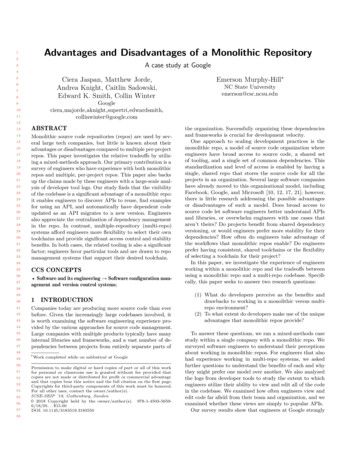
LTC34188A, 4MHz, MonolithicSynchronous nHigh Efficiency: Up to 95%8A Output Current2.25V to 5.5V Input Voltage RangeLow RDS(ON) Internal Switch: 35mΩTracking Input to Provide Easy Supply SequencingProgrammable Frequency: 300kHz to 4MHz0.8V 1% Reference Allows Low Output VoltageQuiescent Current: 380µASelectable Forced Continuous/Burst Mode Operationwith Adjustable Burst ClampSynchronizable Switching FrequencyLow Dropout Operation: 100% Duty CyclePower Good Output Voltage MonitorOvertemperature Protected38-Lead Low Profile (0.75mm) Thermally EnhancedQFN (5mm 7mm) PackageApplicationsnnnnnMicroprocessor, DSP and Memory SuppliesDistributed 2.5V, 3.3V and 5V Power SystemsAutomotive ApplicationsPoint of Load RegulationNotebook ComputersThe LTC 3418 is a high efficiency, monolithic synchronousstep-down DC/DC converter utilizing a constant frequency,current mode architecture. It operates from an input voltagerange of 2.25V to 5.5V and provides a regulated outputvoltage from 0.8V to 5V while delivering up to 8A of outputcurrent. The internal synchronous power switch increasesefficiency and eliminates the need for an external Schottkydiode. Switching frequency is set by an external resistoror can be synchronized to an external clock. OPTI-LOOP compensation allows the transient response to be optimizedover a wide range of loads and output capacitors.The LTC3418 can be configured for either Burst Modeoperation or forced continuous operation. Forced continuous operation reduces noise and RF interferencewhile Burst Mode operation provides high efficiency byreducing gate charge losses at light loads. In Burst Modeoperation, external control of the burst clamp level allowsthe output voltage ripple to be adjusted according to therequirements of the application. A tracking input in theLTC3418 allows for proper sequencing with respect toanother power supply.L, LT, LTC and LTM are registered trademarks of Linear Technology Corporation.Burst Mode and OPTI-LOOP are registered trademarks of Linear Technology Corporation.All other trademarks are the property of their respective owners. Protected by U.S. Patentsincluding 5481178, 6580258, 6304066, 6127815, 6498466, 6611131, 6724174.Typical Application2.5V/8A Step-Down RegulatorEfficiency and Power Loss vs Load Current100CIN47µF 4SVIN TRACK PVIN2.2M30.1k1000pF0.2µHSWCOUT100µF 2LTC3418PGOODPGNDRUN/SSSGNDITH4.99k820pFSYNC/MODE VFB332ΩEFFICIENCY100008070601000POWER LOSS10050404.32k3418 TA01a1.69kVOUT2.5V8A1000001030200.01VIN 3.3VVOUT 2.5V0.11LOAD CURRENT (A)103418 TA01bFor more information www.linear.com/LTC3418POWER LOSS (mW)RT90EFFICIENCY (%)VIN2.8V TO 5.5V13418fc1
LTC3418Absolute Maximum RatingsPin Configuration(Note 1)PGNDPGNDPGNDTRACKPGNDPGNDTOP VIEWPGNDInput Supply Voltage. –0.3V to 6VITH, RUN/SS, VFB Voltages. –0.3V to VINSYNC/MODE Voltages. –0.3V to VINTRACK Voltage. –0.3V to VINSW Voltage. –0.3V to (VIN 0.3V)Operating Temperature Range(Note 2).–40 C to 85 CJunction Temperature (Note 5). 125 CStorage Temperature Range. –65 C to 125 C38 37 36 35 34 33 32SW 131 SWSW 230 SWPVIN 329 PVINPVIN 428 PVINPGOOD 527 SYNC/MODERT 626 ITH39RUN/SS 725 VFBSGND 824 SVINPVIN 923 PVINPVIN 1022 PVINSW 1121 SW20 SWSW 12PGNDPGNDPGNDVREFPGNDPGNDPGND13 14 15 16 17 18 19UHF PACKAGE38-LEAD (7mm 5mm) PLASTIC QFNTJMAX 125 C, θJA 34 C/W, θJC 1 C/WEXPOSED PAD (PIN 39) IS PGND, MUST BE SOLDERED TO PCBorder rderinfoLEAD FREE FINISHTAPE AND REELPART MARKINGPACKAGE DESCRIPTIONTEMPERATURE RANGELTC3418EUHF#PBFLTC3418EUHF#TRPBF341838-Lead (7mm 5mm) Plastic QFN–40 C to 85 CConsult LTC Marketing for parts specified with wider operating temperature ranges.For more information on lead free part marking, go to: http://www.linear.com/leadfree/For more information on tape and reel specifications, go to: http://www.linear.com/tapeandreel/. Some packages are available in 500 unit reels throughdesignated sales channels with #TRMPBF suffix.23418fcFor more information www.linear.com/LTC3418
LTC3418Electrical CharacteristicsThe l denotes the specifications which apply over the full operatingtemperature range, otherwise specifications are at TA 25 C. VIN 3.3V. (Note 2)SYMBOLPARAMETERVINInput Voltage RangeVFBRegulated Feedback VoltageCONDITIONSMINTYP2.250 C TA 85 C(Note 3)IFBFeedback Input Current VFBReference Voltage Line RegulationVIN 2.5V to 5.5V (Note 3)VLOADREGOutput Voltage Load RegulationMeasured in Servo Loop, VITH 0.36VMeasured in Servo Loop, VITH 0.84VVTRACKTracking Voltage OffsetVTRACK 0.4VTracking Voltage 200nA0ITRACKTRACK Input Current100 VPGOODPower Good Range 7.5 9%RPGOODPower Good Resistance100150ΩIQInput DC Bias CurrentActive CurrentShutdown(Note 4)VFB 0.7V, VITH 1VVRUN 0V3800.034501.5µAµAfOSCSwitching FrequencySwitching Frequency RangeROSC 69.8kΩ(Note 6)0.880.311.124MHzMHzfSYNCSYNC Capture Range(Note 6)0.34MHzRPFETRDS(ON) of P-Channel FETISW 600mA3550mΩRNFETRDS(ON) of N-Channel FETISW – 600mA2535mΩILIMITPeak Current LimitVUVLO1217Undervoltage Lockout Threshold1.7522.25VVREFReference Output1.2191.2501.281VILSWSW Leakage Current0.11µAVRUNRUN Threshold0.50.650.8VVRUN 0V, VIN 5.5VNote 1: Stresses beyond those listed under Absolute Maximum Ratingsmay cause permanent damage to the device. Exposure to any AbsoluteMaximum Rating condition for extended periods may affect devicereliability and lifetime.Note 2: The LTC3418 is guaranteed to meet performance specificationsfrom 0 C to 85 C. Specifications over the –40 C to 85 C operatingtemperature range are assured by design, characterization andcorrelation with statistical process controls.ANote 3: The LTC3418 is tested in a feedback loop that adjusts V FB toachieve a specified error amplifier output voltage (ITH).Note 4: Dynamic supply current is higher due to the internal gate chargebeing delivered at the switching frequency.Note 5: TJ is calculated from the ambient temperature TA and powerdissipation PD as follows:LTC3418: TJ TA (PD)(34 C/W)Note 6: This parameter is guaranteed by design and characterization.3418fcFor more information www.linear.com/LTC34183
LTC3418Typical Performance CharacteristicsInternal Reference Voltagevs TemperatureSwitch On-Resistancevs Input VoltageVIN 3.3V5040450.79850.79800.79750.7970VIN 3.3V40350.7990ON-RESISTANCE (mΩ)REFERENCE VOLTAGE (V)0.7995On-Resistance vs Temperature45PFET30ON-RESISTANCE (mΩ)0.8000TA 25 C unless otherwise 60–40 –2002.250–40 –20020 40 60 80TEMPERATURE ( C)100 1202.753.25 3.75 4.25 4.75INPUT VOLTAGE (V)5.253418 G01Quiescent Currentvs Input 253.25 3.75 4.25 4.75INPUT VOLTAGE (V)2.7530025020015032.544.53.5INPUT VOLTAGE (V)960940100108090104010201000980960920920900–40 –209002.25100 1203418 G074100000EFFICIENCY1000070601000POWER LOSS100504010302.753.25 3.75 4.25 4.75INPUT VOLTAGE (V)2502108094020 40 60 80TEMPERATURE ( C)130170ROSC (kΩ)3418 G061100EFFICIENCY (%)FREQUENCY (kHz)98090Efficiency and Power Lossvs Load Current10601000505.253418 G08200.01POWER LOSS (mW)FREQUENCY (kHz)10601020103418 G05VIN 3.3V005.55Frequency vs Input Voltage10401500500Frequency vs Temperature10802000503418 G041100250010005.25VIN 3.3V30001000Frequency vs ROSC3500350FREQUENCY (kHz)QUIESCENT CURRENT (µA)LEAKAGE CURRENT (nA)5001.0100 1203418 G035.01.520 40 60 80TEMPERATURE ( C)3418 G02Switch Leakage vs Input Voltage2.00VIN 3.3VVOUT 2.5V0.11LOAD CURRENT (A)1013418 G093418fcFor more information www.linear.com/LTC3418
LTC3418Typical Performance CharacteristicsEfficiency vs Load Current100Efficiency vs Load Current50403020706050403020VIN 3.3VVOUT 2.5V1000.01FORCED CONTINUOUSVOUT 2.5V00.01100.11LOAD CURRENT (A)3418 G1010–0.058–0.10ΔVOUT/VOUT (%)PEAK INDUCTOR CURRENT (A)0645V0.10.20.3 0.4 0.5VBCLAMP 0–0.30VIN 3.3V20µs/DIVVOUT 2.5VLOAD STEP: 800mA TO 8A0126543LOAD CURRENT (A)73418 G1583418 G14Start-Up DIVINDUCTORCURRENT1A/DIV3418 G16103418 G12Burst Mode OperationINDUCTORCURRENT5A/DIV0.11LOAD CURRENT (A)OUTPUTVOLTAGE100mV/DIV–0.15Load Step TransientOUTPUTVOLTAGE100mV/DIVBurst Mode OPERATIONVOUT 2.5VLoad Step TransientVIN 3.3VVOUT 1.8Vf 1MHz3418 G13VIN 3.3V40µs/DIVVOUT 2.5VLOAD STEP: 3A TO 8A40–0.253.3V050Load Regulation120603418 G11Peak Inductor Currentvs Burst Clamp Voltage27020100.11LOAD CURRENT (A)5V805VEFFICIENCY (%)FORCED CONTINUOUS603.3V903.3V80EFFICIENCY (%)EFFICIENCY (%)100908070Efficiency vs Load Current100Burst Mode OPERATION90TA 25 C unless otherwise noted.INDUCTORCURRENT2A/DIVVIN 3.3VVOUT 2.5VLOAD: 200mA20µs/DIV3418 G17VIN 3.3VVOUT 2.5VLOAD: 8A1ms/DIV3418 G183418fcFor more information www.linear.com/LTC34185
LTC3418Pin FunctionsSW (Pins 1, 2, 11, 12, 20, 21, 30, 31): Switch Node Connection to Inductor. This pin connects to the drains of theinternal main and synchronous power MOSFET switches.PVIN (Pins 3, 4, 9, 10, 22, 23, 28, 29): Power InputSupply. Decouple these pins to PGND with capacitors onall four corners of the package.PGOOD (Pin 5): Power Good Output. Open-drain logicoutput that is pulled to ground when the output voltageis not within 7.5% of regulation point.VREF (Pin 16): Reference Output. Decouple this pin witha 2.2µF capacitor.SVIN (Pin 24): Signal Input Supply. Decouple this pin toSGND with a capacitor.VFB (Pin 25): Feedback Pin. Receives the feedback voltage from a resistive divider connected across the output.RT (Pin 6): Oscillator Resistor Input. Connecting a resistor to ground from this pin sets the switching frequency.ITH (Pin 26): Error Amplifier Compensation Point. Thecurrent comparator threshold increases with this controlvoltage. Nominal voltage range for this pin is from 0.2Vto 1.4V with 0.4V corresponding to the zero-sense voltage(zero current).RUN/SS (Pin 7): Run Control and Soft-Start Input. Forcingthis pin below 0.5V shuts down the LTC3418. In shutdownall functions are disabled drawing 1.5µA of supply current. A capacitor to ground from this pin sets the ramptime to full output current.SYNC/MODE (Pin 27): Mode Select and External ClockSynchronization Input. To select Forced Continuous, tieto SVIN. Connecting this pin to a voltage between 0V and1V selects Burst Mode operation with the burst clamp setto the pin voltage.SGND (Pin 8): Signal Ground. All small-signal componentsand compensation components should connect to thisground, which in turn connects to PGND at one point.TRACK (Pin 35): Voltage Tracking Input. Feedback voltage will regulate to the voltage on this pin during start-uppower sequencing.PGND (Pins 13, 14, 15, 17, 18, 19, 32, 33, 34, 36, 37,38): Power Ground. Connect this pin closely to the (–)terminal of CIN and COUT.Exposed Pad (Pin 39): The Exposed Pad is PGND and mustbe soldered to the PCB ground for electrical connectionand rated thermal performance.63418fcFor more information www.linear.com/LTC3418
LTC3418Block AMPLIFIER–VFBPMOS CURRENTCOMPARATORSLOPECOMPENSATIONRECOVERYTRACK 2526SGNDBCLAMPBURSTCOMPARATOR SECOMPARATORSYNC/MODERT627 5231022SW12111220213031 LOGICRUN/SS9SLOPECOMPENSATIONOSCILLATOR 728 –0.86V4–SYNC/MODE 29 –0.74V3PGND1332143315341736183719383418 BD3418fcFor more information www.linear.com/LTC34187
LTC3418OPERATIONMain Control LoopBurst Mode OperationThe LTC3418 is a monolithic, constant frequency, currentmode step-down DC/DC converter. During normal operation, the internal top power switch (P-channel MOSFET) isturned on at the beginning of each clock cycle. Current inthe inductor increases until the current comparator tripsand turns off the top power MOSFET. The peak inductorcurrent at which the current comparator shuts off the toppower switch is controlled by the voltage on the ITH pin.The error amplifier adjusts the voltage on the ITH pin bycomparing the feedback signal from a resistor divider onthe VFB pin with an internal 0.8V reference. When the loadcurrent increases, it causes a reduction in the feedbackvoltage relative to the reference. The error amplifier raisesthe ITH voltage until the average inductor current matchesthe new load current. When the top power MOSFET shutsoff, the synchronous power switch (N-channel MOSFET)turns on until either the bottom current limit is reached orthe beginning of the next clock cycle. The bottom currentlimit is set at –8A for force continuous mode and 0A forBurst Mode operation.Connecting the SYNC/MODE pin to a voltage in the rangeof 0V to 1V enables Burst Mode operation. In Burst Modeoperation, the internal power MOSFETs operate intermittently at light loads. This increases efficiency by minimizing switching losses. During Burst Mode operation, theminimum peak inductor current is externally set by thevoltage on the SYNC/MODE pin and the voltage on the ITHpin is monitored by the burst comparator to determinewhen sleep mode is enabled and disabled. When theaverage inductor current is greater than the load current,the voltage on the ITH pin drops. As the ITH voltage fallsbelow 350mV, the burst comparator trips and enablessleep mode. During sleep mode, the top power MOSFETis held off while the load current is solely supplied by theoutput capacitor. When the output voltage drops, the topand bottom power MOSFETs begin switching to bring theoutput back into regulation. This process repeats at a ratethat is dependent on the load demand.The operating frequency is externally set by an externalresistor connected between the RT pin and ground. Thepractical switching frequency can range from 300kHz to4MHz.Overvoltage and undervoltage comparators will pull thePGOOD output low if the output voltage comes out ofregulation by 7.5%. In an overvoltage condition, the toppower MOSFET is turned off and the bottom power MOSFETis switched on until either the overvoltage condition clearsor the bottom MOSFET’s current limit is reached.Forced ContinuousConnecting the SYNC/MODE pin to SVIN will disable BurstMode operation and force continuous current operation.At light loads, forced continuous mode operation is lessefficient than Burst Mode operation, but may be desirable insome applications where it is necessary to keep switchingharmonics out of a signal band. The output voltage rippleis minimized in this mode.8Pulse skipping operation can be implemented by connecting the SYNC/MODE pin to ground. This forces the burstclamp level to be at 0V. As the load current decreases, thepeak inductor current will be determined by the voltageon the ITH pin until the ITH voltage drops below 400mV. Atthis point, the peak inductor current is determined by theminimum on-time of the current comparator. If the loaddemand is less than the average of the minimum on-timeinductor current, switching cycles will be skipped to keepthe output voltage in regulation.Frequency SynchronizationThe internal oscillator of the LTC3418 can by synchronizedto an external clock connected to the SYNC/MODE pin.The frequency of the external clock can be in the rangeof 300kHz to 4MHz.For this application, the oscillator timing resistor shouldbe chosen to correspond to a frequency that is 25% lowerthan the synchronization frequency. During synchronization, the burst clamp is set to 0V, and each switching cyclebegins at the falling edge of the clock signal.3418fcFor more information www.linear.com/LTC3418
LTC3418OperationDropout OperationShort-Circuit ProtectionWhen the input supply voltage decreases toward the outputvoltage, the duty cycle increases toward the maximumon-time. Further reduction of the supply voltage forcesthe main switch to remain on for more than one cycleeventually reaching 100% duty cycle. The output voltagewill then be determined by the input voltage minus thevoltage drop across the internal P-channel MOSFET andthe inductor.When the output is shorted to ground, the inductor current decays very slowly during a single switching cycle.To prevent current runaway from occurring, a secondarycurrent limit is imposed on the inductor current. If theinductor valley current increases larger than 15A, the toppower MOSFET will be held off and switching cycles willbe skipped until the inductor current is reduced.Low Supply OperationThe LTC3418 is designed to operate down to an input supply voltage of 2.25V. One important consideration at lowinput supply voltages is that the RDS(ON) of the P‑channeland N-channel power switches increases. The user shouldcalculate the power dissipation when the LTC3418 is usedat 100% duty cycle with low input voltages to ensure thatthermal limits are not exceeded.Slope Compensation and Inductor Peak CurrentSlope compensation provides stability in constant frequency architectures by preventing subharmonic oscillations at duty cycles greater than 50%. It is accomplishedinternally by adding a compensating ramp to the inductorcurrent signal. Normally, the maximum inductor peakcurrent is reduced when slope compensation is added.In the LTC3418, however, slope compensation recoveryis implemented to keep the maximum inductor peak current constant throughout the range of duty cycles. Thiskeeps the maximum output current relatively constantregardless of duty cycle.Voltage TrackingSome microprocessors and DSP chips need two powersupplies with different voltage levels. These systems oftenrequire voltage sequencing between the core power supply and the I/O power supply. Without proper sequencing,latch-up failure or excessive current draw may occur thatcould result in damage to the processor’s I/O ports or theI/O ports of a supporting system device such as memory,an FPGA or a data converter. To ensure that the I/O loadsare not driven until the core voltage is properly biased,tracking of the core supply and the I/O supply voltage isnecessary.Voltage tracking is enabled by applying a ramp voltageto the TRACK pin. When the voltage on the TRACK pinis below 0.8V, the feedback voltage will regulate to thistracking voltage. When the tracking voltage exceeds 0.8V,control over the feedback voltage is gradually released.Full release of tracking control over the feedback voltageis achieved when the tracking voltage exceeds 1.05V.Voltage Reference OutputThe LTC3418 provides a 1.25V reference voltage that iscapable of sourcing up to 5mA of output current. Thisreference voltage is generated from a linear regulator andis intended for applications requiring a low noise referencevoltage. To ensure that the output is stable, the referencevoltage pin should be decoupled with a minimum of 2.2µF.3418fcFor more information www.linear.com/LTC34189
LTC3418APPLICATIONS INFORMATIONThe basic LTC3418 application circuit is shown on thefront page of this data sheet. External component selectionis determined by the maximum load current and beginswith the selection of the operating frequency and inductorvalue followed by CIN and COUT.Having a lower ripple current reduces the core losses inthe inductor, the ESR losses in the output capacitors andthe output voltage ripple. Highest efficiency operation isachieved at low frequency with small ripple current. This,however, requires a large inductor.Operating FrequencyA reasonable starting point for selecting the ripple currentis IL 0.4(IMAX). The largest ripple current occurs at thehighest VIN. To guarantee that the ripple current staysbelow a specified maximum, the inductor value shouldbe chosen according to the following equation:Selection of the operating frequency is a trade-off betweenefficiency and component size. High frequency operationallows the use of smaller inductor and capacitor values.Operation at lower frequencies improves efficiency byreducing internal gate charge losses but requires largerinductance values and/or capacitance to maintain lowoutput ripple voltage.The operating frequency of the LTC3418 is determinedby an external resistor that is connected between the RTpin and ground. The value of the resistor sets the rampcurrent that is used to charge and discharge an internaltiming capacitor within the oscillator and can be calculatedby using the following equation:R OSC 7.3 1010 Ω – 2.5kΩfAlthough frequencies as high as 4MHz are possible, theminimum on-time of the LTC3418 imposes a minimumlimit on the operating duty cycle. The minimum on-timeis typically 80ns. Therefore, the minimum duty cycle isequal to:100 80ns f(Hz)Inductor SelectionFor a given input and output voltage, the inductor valueand operating frequency determine the ripple current. Theripple current IL increases with higher VIN or VOUT anddecreases with higher inductance: V V ΔIL OUT 1– OUT VIN fL 10 VVL OUT 1– OUT fΔIL(MAX) VIN(MAX) The inductor value will also have an effect on Burst Modeoperation. The transition from low current operation begins when the peak inductor current falls below a levelset by the burst clamp. Lower inductor values result inhigher ripple current which causes this to occur at lowerload currents. This causes a dip in efficiency in the upperrange of low current operation. In Burst Mode operation,lower inductance values will cause the burst frequencyto increase.Inductor Core SelectionOnce the value for L is known, the type of inductor mustbe selected. Actual core loss is independent of core sizefor a fixed inductor value, but it is very dependent on theinductance selected. As the inductance increases, corelosses decrease. Unfortunately, increased inductancerequires more turns of wire and therefore copper losseswill increase.Ferrite designs have very low core losses and are preferred at high switching frequencies, so design goals canconcentrate on copper loss and preventing saturation.Ferrite core material saturates “hard,” which means thatinductance collapses abruptly when the peak design currentis exceeded. This results in an abrupt increase in inductorripple current and consequent output voltage ripple. Donot allow the core to saturate!3418fcFor more information www.linear.com/LTC3418
LTC3418APPLICATIONS INFORMATIONDifferent core materials and shapes will change the size/current and price/current relationship of an inductor. Toroidor shielded pot cores in ferrite or permalloy materials aresmall and don’t radiate much energy, but generally costmore than powdered iron core inductors with similarcharacteristics. The choice of which style inductor to usemainly depends on the price vs size requirements and anyradiated field/EMI requirements. New designs for surfacemount inductors are available from Coiltronics, Coilcraft,Toko and Sumida.CIN and COUT SelectionThe input capacitance, CIN, is needed to filter the trapezoidalwave current at the source of the top MOSFET. To preventlarge voltage transients from occurring, a low ESR inputcapacitor sized for the maximum RMS current should beused. The maximum RMS current is given by:I RMS I OUT(MAX)VOUTVINVIN–1VOUTThis formula has a maximum at VIN 2VOUT, where IRMS IOUT/2. This simple worst-case condition is commonly usedfor design because even significant deviations do not offermuch relief. Note that ripple current ratings from capacitormanufacturers are often based on only 2000 hours of lifewhich makes it advisable to further derate the capacitor,or choose a capacitor rated at a higher temperature thanrequired. Several capacitors may also be paralleled to meetsize or height requirements in the design.The selection of COUT is determined by the effective seriesresistance (ESR) that is required to minimize voltage rippleand load step transients as well as the amount of bulkcapacitance that is necessary to ensure that the controlloop is stable. Loop stability can be checked by viewingthe load transient response as described in a later section.The output ripple, VOUT, is determined by: 1 ΔVOUT ΔIL ESR 8fCOUT RMS current handling requirements. Dry tantalum, specialpolymer, aluminum electrolytic and ceramic capacitors areall available in surface mount packages. Special polymercapacitors offer very low ESR but have lower capacitancedensity than other types. Tantalum capacitors have thehighest capacitance density but it is important to onlyuse types that have been surge tested for use in switchingpower supplies. Aluminum electrolytic capacitors havesignificantly higher ESR, but can be used in cost-sensitiveapplications provided that consideration is given to ripplecurrent ratings and long term reliability. Ceramic capacitors have excellent low ESR characteristics but can havea high voltage coefficient and audible piezoelectric effects.The high Q of ceramic capacitors with trace inductancecan also lead to significant ringing.Using Ceramic Input and Output CapacitorsHigher values, lower cost ceramic capacitors are nowbecoming available in smaller case sizes. Their high ripplecurrent, high voltage rating and low ESR make them idealfor switching regulator applications. However, care mustbe taken when these capacitors are used at the input andoutput. When a ceramic capacitor is used at the input andthe power is supplied by a wall adapter through long wires,a load step at the output can induce ringing at the input,VIN. At best, this ringing can couple to the output and bemistaken as loop instability. At worst, a sudden inrushof current through the long wires can potentially causea voltage spike at VIN large enough to damage the part.When choosing the input and output ceramic capacitors,choose the X5R or X7R dielectric formulations. Thesedielectrics have the best temperature and voltage characteristics of all the ceramics for a given value and size.Output Voltage ProgrammingThe output voltage is set by an external resistive divideraccording to the following equation: R2 VOUT 0.8 1 R1 The output ripple is highest at maximum input voltagesince IL increases with input voltage. Multiple capacitorsplaced in parallel may be needed to meet the ESR andThe resistive divider allows pin VFB to sense a fraction ofthe output voltage as shown in Figure 1.3418fcFor more information www.linear.com/LTC341811
LTC3418APPLICATIONS INFORMATIONpin to ground. This sets IBURST to 0A. In this condition, thepeak inductor current is limited by the minimum on-timeof the current comparator; and the lowest output voltageripple is achieved while still operating discontinuously.During very light output loads, pulse skipping allows onlya few switching cycles to be skipped while maintainingthe output voltage in regulation.VFBLTC3418R1SGND3418 F01Figure 1. Setting the Output VoltageBurst Clamp ProgrammingIf the voltage on the SYNC/MODE pin is less than VIN by1V, Burst Mode operation is enabled. During Burst Modeoperation, the voltage on the SYNC/MODE pin determinesthe burst clamp level, which sets the minimum peak inductor current, IBURST, for each switching cycle. A graphshowing the relationship between the minimum peakinductor current and the voltage on the SYNC/MODE pincan be found in the Typical Performance Characteristicssection. In the graph, VBURST is the voltage on the SYNC/MODE pin. IBURST can only be programmed in the rangeof 0A to 10A. For values of VBURST less than 0.4V, IBURSTis set at 0A. As the output load current drops, the peakinductor currents decrease to keep the output voltage inregulation. When the output load current demands a peakinductor current that is less than IBURST, the burst clamp willforce the peak inductor current to remain equal to IBURSTregardless of further reductions in the load current. Sincethe average inductor current is greater than the output loadcurrent, the voltage on the ITH pin will decrease. Whenthe ITH voltage drops to 350mV, sleep mode is enabledin which both power MOSFETs are shut off and switchingaction is discontinued to minimize power consumption.All circuitry is turned back on and the power MOSFETsbegin switching again when the output voltage drops outof regulation. The value for IBURST is determined by thedesired amount of output voltage ripple. As the value ofIBURST increases, the sleep period between pulses and theoutput voltage ripple increase. The burst clamp voltage,VBURST, can be set by a resistor divider from the VFB pinto the SGND pin as shown in the Typical Application onthe front page of this data sheet.Pulse skipping, which is a compromise between low outputvoltage ripple and efficiency during low load current operation, can be implemented by connecting the SYNC/MODE12Voltage TrackingThe LTC3418 allows the user to program how its outputvoltage ramps during start-up by means of the TRACKpin. Through this pin, the output voltage can be set up toeither track coincidentally or ratiometrically follow anotheroutput voltage as shown in Figure 2. If the voltage on theTRACK pin is less than 0.8V, voltage tracking is enabled.During voltage tracking, the output voltage regulates tothe tracking voltage through a resistor divider network.VOUT2OUTPUT VOLTAGER2VOUT1TIME3418 F02aFigure 2a. Coincident TrackingVOUT2OUTPUT VOLTAGEVOUTVOUT1TIME3418 F02aFigure 2b. Ratiometric SequencingFor more information www.linear.com/LTC34183418fc
LTC3418APPLICATIONS INFORMATIONThe output voltage during tracking can be calculated withthe following equation: R2 VOUT VTRACK 1 ,VTRACK 0.8V R1 To implement the coincident tracking in Figure 2a, connect an extra resistor divider to the output of VOUT2 andconnect its midpoint to the TRACK pin of the LTC3418as shown in Figure 3. The ratio of this divider should beselected the same as that of VOUT1’s resistor divider. Toimplement the ratiometr
4500 3418 G06 1000 50 90 130 210 250 3000 3500 4000 VIN 3.3V Efficiency and Power Loss vs Load Current LOAD CURRENT (A) 0.01 EFFICIENCY (%) 60 POWER LOSS (mW) 80 100 0.1 1 10 3418 G09 40 50 70 90 30 20 1000 100000 100 10000 10 1 EFFICIENCY POWER LOSS VIN 3.3V VOUT 2.5V TA 25 C unless otherwise noted. Switch On-Resistance