Transcription
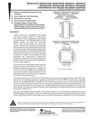
SN54ALS161B, SN54ALS162B, SN54ALS163B, SN54AS161, SN54AS163SN74ALS161B, SN74ALS163B, SN74AS161, SN74AS163SYNCHRONOUS 4-BIT DECADE AND BINARY COUNTERSSDAS276A – DECEMBER 1994 – REVISED JULY 2000DDDDDInternal Look-Ahead Circuitry for FastCountingCarry Output for n-Bit CascadingSynchronous CountingSynchronously ProgrammablePackage Options Include PlasticSmall-Outline (D) and Shrink Small-Outline(DB) Packages, Ceramic Chip Carriers (FK),Standard Plastic (N) and Ceramic (J) DIPsSN54ALS161B, SN54ALS162B, SN54ALS163B,SN54AS161, SN54AS163 . . . J PACKAGESN74ALS161B, SN74AS161,SN74AS163 . . . D OR N PACKAGESN74ALS163B . . . D, DB, OR N PACKAGE(TOP VIEW)CLRCLKABCDENPGNDdescriptionThese counters are fully programmable; they canbe preset to any number between 0 and 9 or 15.Because presetting is synchronous, setting up alow level at the load (LOAD) input disables thecounter and causes the outputs to agree with thesetup data after the next clock pulse, regardlessof the levels of the enable CLKCLRNCVCCRCOSN54ALS161B, SN54ALS162B, SN54ALS163B,SN54AS161, SN54AS163 . . . FK PACKAGE(TOP VIEW)ABNCCD43 2 1 20 19185176167158149 10 11 12 13QAQBNCQCQDENPGNDNCLOADENTThese synchronous, presettable, 4-bit decadeand binary counters feature an internal carrylook-ahead circuitry for application in high-speedcounting designs. The SN54ALS162B is a 4-bitdecade counter. The ’ALS161B, ’ALS163B,’AS161, and ’AS163 devices are 4-bit binarycounters. Synchronous operation is provided byhaving all flip-flops clocked simultaneously so thatthe outputs change coincidentally with each otherwhen instructed by the count-enable (ENP, ENT)inputs and internal gating. This mode of operationeliminates the output counting spikes normallyassociated with asynchronous (ripple-clock)counters. A buffered clock (CLK) input triggers thefour flip-flops on the rising (positive-going) edge ofthe clock input waveform.1NC – No internal connectionThe clear function for the ’ALS161B and ’AS161 devices is asynchronous. A low level at the clear (CLR) inputsets all four of the flip-flop outputs low, regardless of the levels of the CLK, LOAD, or enable inputs. The clearfunction for the SN54ALS162B, ’ALS163B, and ’AS163 devices is synchronous, and a low level at CLR setsall four of the flip-flop outputs low after the next clock pulse, regardless of the levels of the enable inputs. Thissynchronous clear allows the count length to be modified easily by decoding the Q outputs for the maximumcount desired. The active-low output of the gate used for decoding is connected to CLR to synchronously clearthe counter to 0000 ( LLLL ).The carry look-ahead circuitry provides for cascading counters for n-bit synchronous applications withoutadditional gating. ENP and ENT inputs and a ripple-carry (RCO) output are instrumental in accomplishing thisfunction. Both ENP and ENT must be high to count, and ENT is fed forward to enable RCO. RCO, thus enabled,Please be aware that an important notice concerning availability, standard warranty, and use in critical applications ofTexas Instruments semiconductor products and disclaimers thereto appears at the end of this data sheet.Copyright 2000, Texas Instruments IncorporatedPRODUCTION DATA information is current as of publication date.Products conform to specifications per the terms of Texas Instrumentsstandard warranty. Production processing does not necessarily includetesting of all parameters.On products compliant to MIL-PRF-38535, all parameters are testedunless otherwise noted. On all other products, productionprocessing does not necessarily include testing of all parameters.POST OFFICE BOX 655303 DALLAS, TEXAS 752651
SN54ALS161B, SN54ALS162B, SN54ALS163B, SN54AS161, SN54AS163SN74ALS161B, SN74ALS163B, SN74AS161, SN74AS163SYNCHRONOUS 4-BIT DECADE AND BINARY COUNTERSSDAS276A – DECEMBER 1994 – REVISED JULY 2000description (continued)produces a high-level pulse while the count is maximum (9 or 15, with QA high). The high-level overflowripple-carry pulse can be used to enable successive cascaded stages. Transitions at ENP or ENT are allowed,regardless of the level of CLK.These counters feature a fully independent clock circuit. Changes at control inputs (ENP, ENT, or LOAD) thatmodify the operating mode have no effect on the contents of the counter until clocking occurs. The function ofthe counter (whether enabled, disabled, loading, or counting) is dictated solely by the conditions meeting thestable setup and hold times.The SN54ALS161B, SN54ALS162B, SN54ALS163B, SN54AS161, and SN54AS163 are characterized foroperation over the full military temperature range of – 55 C to 125 C. The SN74ALS161B, SN74ALS163B,SN74AS161, and SN74AS163 are characterized for operation from 0 C to 70 C.logic symbols†’ALS161B AND ’AS161 BINARY COUNTERSWITH DIRECT CLEAR1CLR9LOADENTENPCLKABCD10723456’ALS163B AND ’AS163 BINARY COUNTERSWITH SYNCHRONOUS CLEARCTRDIV16CT 0M1M2153CT 15RCOENTG4ENPC5/2,3,4 CLK14[1]13[2]12[4]11[8]9M1M2LOADG31, 5DCTRDIV165CT C5/2,3,4 31, 5D [1]4[2]5[4]63CT 9[8]15G4C5/2,3,4 [1][2][4][8]14131211† These symbols are in accordance with ANSI/IEEE Std 91-1984 and IEC Publication 617-12.Pin numbers shown are for the D, DB, J, and N packages.2RCOG31, 5DPOST OFFICE BOX 655303 DALLAS, TEXAS 75265RCOG42CTRDIV105CT 0115G3SN54ALS162B DECADE COUNTERWITH SYNCHRONOUS CLEARCLR3CT 15QAQBQCQD14131211QAQBQCQD
SN54ALS161B, SN54ALS162B, SN54ALS163B, SN54AS161, SN54AS163SN74ALS161B, SN74ALS163B, SN74AS161, SN74AS163SYNCHRONOUS 4-BIT DECADE AND BINARY COUNTERSSDAS276A – DECEMBER 1994 – REVISED JULY 2000logic diagram (positive 1DA3C113QB1DB4C112QC1DC5C111QD1DD6Pin numbers shown are for the J package.POST OFFICE BOX 655303 DALLAS, TEXAS 752653
SN54ALS161B, SN54ALS162B, SN54ALS163B, SN54AS161, SN54AS163SN74ALS161B, SN74ALS163B, SN74AS161, SN74AS163SYNCHRONOUS 4-BIT DECADE AND BINARY COUNTERSSDAS276A – DECEMBER 1994 – REVISED JULY 2000logic diagram (positive logic)CLRLOADENTENPCLK1’ALS163B and 1DD6Pin numbers shown are for the D, DB, J, and N packages.’ALS161B and ’AS161 synchronous binary counters are similar; however, CLR is asynchronous.4POST OFFICE BOX 655303 DALLAS, TEXAS 7526511QD
SN54ALS161B, SN54ALS162B, SN54ALS163B, SN54AS161, SN54AS163SN74ALS161B, SN74ALS163B, SN74AS161, SN74AS163SYNCHRONOUS 4-BIT DECADE AND BINARY COUNTERSSDAS276A – DECEMBER 1994 – REVISED JULY 2000typical clear, preset, count, and inhibit sequencesSN54ALS162BThe following sequence is illustrated below:1. Clear outputs to zero (SN54ALS162B is synchronous)2. Preset to BCD 73. Count to 8, 9, 0, 1, 2, and 34. QBQCQDRCO7890123CountInhibitSync PresetClearAsyncClearPOST OFFICE BOX 655303 DALLAS, TEXAS 752655
SN54ALS161B, SN54ALS162B, SN54ALS163B, SN54AS161, SN54AS163SN74ALS161B, SN74ALS163B, SN74AS161, SN74AS163SYNCHRONOUS 4-BIT DECADE AND BINARY COUNTERSSDAS276A – DECEMBER 1994 – REVISED JULY 2000typical clear, preset, count, and inhibit sequences’ALS161B, ’AS161, ’ALS163B, and ’AS163The following sequence is illustrated below:1. Clear outputs to zero (’ALS161B and ’AS161 are asynchronous; ’ALS163B and ’AS163 aresynchronous.)2. Preset to binary 123. Count to 13, 14, 15, 0, 1, and 24. QBQCQDRCO12131415012CountSync PresetClearAsyncClear6POST OFFICE BOX 655303 DALLAS, TEXAS 75265Inhibit
SN54ALS161B, SN54ALS162B, SN54ALS163B, SN54AS161, SN54AS163SN74ALS161B, SN74ALS163B, SN74AS161, SN74AS163SYNCHRONOUS 4-BIT DECADE AND BINARY COUNTERSSDAS276A – DECEMBER 1994 – REVISED JULY 2000absolute maximum ratings over operating free-air temperature range (unless otherwise noted)†Supply voltage range, VCC . . . . . . . . . . . . . . . . . . . . . . . . . . . . . . . . . . . . . . . . . . . . . . . . . . . . . . . . . . –0.5 V to 7 VInput voltage range, VI . . . . . . . . . . . . . . . . . . . . . . . . . . . . . . . . . . . . . . . . . . . . . . . . . . . . . . . . . . . . . . –0.5 V to 7 VPackage thermal impedance, θJA (see Note 1): D package . . . . . . . . . . . . . . . . . . . . . . . . . . . . . . . . . . . 73 C/WDB package . . . . . . . . . . . . . . . . . . . . . . . . . . . . . . . . . 82 C/WN package . . . . . . . . . . . . . . . . . . . . . . . . . . . . . . . . . . . 67 C/WStorage temperature range, Tstg . . . . . . . . . . . . . . . . . . . . . . . . . . . . . . . . . . . . . . . . . . . . . . . . . . . – 65 C to 150 C† Stresses beyond those listed under “absolute maximum ratings” may cause permanent damage to the device. These are stress ratings only, andfunctional operation of the device at these or any other conditions beyond those indicated under “recommended operating conditions” is notimplied. Exposure to absolute-maximum-rated conditions for extended periods may affect device reliability.NOTE 1: The package thermal impedance is calculated in accordance with JESD 51.recommended operating upply voltageVILIOHLow-level input voltageIOLTAHigh-level input X4.555.54.555.522VV0.70.8High-level output current– 0.4– 0.4mALow-level output current48mA70 COperating free-air temperature– 551250Velectrical characteristics over recommended operating free-air temperature range (unlessotherwise noted)PARAMETERTEST CONDITIONSVIKVOHVCC 4.5 V,VCC 4.5 V to 5.5 V,II – 18 mAIOH – 0.4 mAVOLVCC 44.55VIOL 4 mAIOL 8 mAIIIIHVCC 5.5 V,VCC 5.5 V,VI 7 VVI 2.7 VIILIO§VCC 5.5 V,VCC 5.5 V,VI 0.4 VVO 2.25 VSN54ALS161BSN54ALS162BSN54ALS163BMIN TYP‡MAXSN74ALS161BSN74ALS163BMINTYP‡– 1.5VCC – 2MAX– 1.5VCC – 20.25– 20UNIT0.4VV0.250.40.350.5V0.10.12020µA– 0.2– 0.2mA– 112mA– 112– 30mAICCVCC 5.5 V12211221mA‡ All typical values are at VCC 5 V, TA 25 C.§ The output conditions have been chosen to produce a current that closely approximates one-half of the true short-circuit output current, IOS.POST OFFICE BOX 655303 DALLAS, TEXAS 752657
SN54ALS161B, SN54ALS162B, SN54ALS163B, SN54AS161, SN54AS163SN74ALS161B, SN74ALS163B, SN74AS161, SN74AS163SYNCHRONOUS 4-BIT DECADE AND BINARY COUNTERSSDAS276A – DECEMBER 1994 – REVISED JULY 2000timing requirements over recommended operating conditions (unless otherwise noted) (seeFigure lock frequencyPulse durationSetup time, before CLK MIN22CLR high or low12.52015A, B, C, D5015LOAD2015’ALS161B2515’ALS161BCLR lowSN54ALS162B, ’ALS163BSN54ALS162B ’ALS163BSN54ALS162B,ENP ENTENP,2015CLR inactive1010CLR low2015CLR high201000Hold time, all synchronous inputs after CLK znsnsnsswitching characteristics over recommended operating conditions (unless otherwise noted) (seeFigure 20419415625620318313317313Any Q827824RCO11321123RCOCLKAny QENTRCOUNITMHz5CLKCLRSN74ALS161Bnsnsnsnsswitching characteristics over recommended operating conditions (unless otherwise noted) (seeFigure Any QENTRCOPOST OFFICE BOX 655303 DALLAS, TEXAS 25620316313316313nsnsns
SN54ALS161B, SN54ALS162B, SN54ALS163B, SN54AS161, SN54AS163SN74ALS161B, SN74ALS163B, SN74AS161, SN74AS163SYNCHRONOUS 4-BIT DECADE AND BINARY COUNTERSSDAS276A – DECEMBER 1994 – REVISED JULY 2000recommended operating MINNOMMAXMINNOMMAX4.555.54.555.5VCCVIHSupply voltageVILIOHLow-level input voltage0.80.8VHigh-level output current–2–2mAIOLTALow-level output current2020mA70 CHigh-level input voltage2Operating free-air temperature2– 55125VV0electrical characteristics over recommended operating free-air temperature range (unlessotherwise noted)PARAMETERSN54AS161SN54AS163TEST CONDITIONSMINVIKVOHVCC 4.5 V,VCC 4.5 V to 5.5 V,II – 18 mAIOH – 2 mAVOLVCC 4.5 V,IOL 20 mAVCC 5.5 V,VI 7 VTYP†ENTVCC 5.5 V,VI 2.7 VAll othersLOADIILENTVCC 5.5 V,TYP†VI 0.4 VAll othersUNITMAX– 1.2VCC – 20.25LOADENTMIN– 1.2All othersIIHMAXVCC – .10.1606040402020–1.5–1.5–1–1– 0.5– 0.5VmAµAmAIO‡VCC 5.5 V,VO 2.25 V– 30– 112– 30– 112mAICCVCC 5.5 V35533553mA† All typical values are at VCC 5 V, TA 25 C.‡ The output conditions have been chosen to produce a current that closely approximates one half of the true short-circuit output current, IOS.POST OFFICE BOX 655303 DALLAS, TEXAS 752659
SN54ALS161B, SN54ALS162B, SN54ALS163B, SN54AS161, SN54AS163SN74ALS161B, SN74ALS163B, SN74AS161, SN74AS163SYNCHRONOUS 4-BIT DECADE AND BINARY COUNTERSSDAS276A – DECEMBER 1994 – REVISED JULY 2000timing requirements over recommended operating conditions (see Figure 1)SN54AS161SN54AS163MINfclockClock frequencytwPulse durationtsuSetup time,time before CLK MIN65CLR high or low6.7108A, B, C, D108LOAD108ENP, ENT108CLR inactive108CLR low1412CLR high (inactive)10920CLR low’AS161Hold time, all synchronous inputs after CLK 3MHznsnsnsswitching characteristics over recommended operating conditions (see Figure X7518.518317.5316.5CLKRCO214212.5CLKAny Q17.517214213RCO1.5101.59ENT19.518.5Any Q214213RCO214212.5CLRUNITMHzRCO (with LOAD low)tPHLtPLHtPHLMAXRCO (with LOAD high)CLKtPHLMIN65*tPLHtPHLtPLHSN54AS161nsnsnsnsns* On products compliant to MIL-PRF-38535, this parameter is not production tested.switching characteristics over recommended operating conditions (see Figure CLKSN74AS163MINMAX7518.518RCO (with LOAD 18.5CLKAny QPOST OFFICE BOX 655303 DALLAS, TEXAS 75265UNITMHzRCO (with LOAD high)RCOENTtPHL* On products compliant to MIL-PRF-38535, this parameter is not production tested.10MIN65*tPLHtPHLtPLHSN54AS163nsnsnsns
SN54ALS161B, SN54ALS162B, SN54ALS163B, SN54AS161, SN54AS163SN74ALS161B, SN74ALS163B, SN74AS161, SN74AS163SYNCHRONOUS 4-BIT DECADE AND BINARY COUNTERSSDAS276A – DECEMBER 1994 – REVISED JULY 2000PARAMETER MEASUREMENT INFORMATIONSERIES 54ALS/74ALS AND 54AS/74AS DEVICES7VVCCFrom OutputUnder TestFrom OutputUnder TestTestPoint500 ΩCL 50 pF(see Note A)500 ΩTestPoint500 Ω3V500 ΩLOAD CIRCUITFOR 3-STATE OUTPUTSLOAD CIRCUITFOR OPEN-COLLECTOR OUTPUTS3VHigh-LevelPulse1.5 VTestPointFrom OutputUnder TestCL 50 pF(see Note A)CL 50 pF(see Note A)LOAD CIRCUIT FORBI-STATE TOTEM-POLE OUTPUTSTimingInputS11.5 V1.5 V0V0Vtwthtsu3VDataInput1.5 V3VLow-LevelPulse1.5 V0V1.5 V0VVOLTAGE WAVEFORMSPULSE DURATIONSVOLTAGE WAVEFORMSSETUP AND HOLD TIMESOutputControl(low-levelenabling)3V1.5 V1.5 V0VtPZL1.5 VtPHZVOL0.3 VtPZHVOH1.5 V3VInputtPLZ 3 VWaveform 1S1 Closed(see Note B)Waveform 2S1 Open(see Note B)1.5 V0.3 V 0 VVOLTAGE WAVEFORMSENABLE AND DISABLE TIMES, 3-STATE OUTPUTS1.5 V1.5 V0VtPLHIn-PhaseOutputtPHLVOH1.5 VVOLtPHLOut-of-PhaseOutput(see Note C)1.5 VtPLHVOH1.5 V1.5 VVOLVOLTAGE WAVEFORMSPROPAGATION DELAY TIMESNOTES: A. CL includes probe and jig capacitance.B. Waveform 1 is for an output with internal conditions such that the output is low except when disabled by the output control.Waveform 2 is for an output with internal conditions such that the output is high except when disabled by the output control.C. When measuring propagation delay items of 3-state outputs, switch S1 is open.D. All input pulses have the following characteristics: PRR 1 MHz, tr tf 2 ns, duty cycle 50%.E. The outputs are measured one at a time with one input transition per measurement.Figure 1. Load Circuits and Voltage WaveformsPOST OFFICE BOX 655303 DALLAS, TEXAS 7526511
SN54ALS161B, SN54ALS162B, SN54ALS163B, SN54AS161, SN54AS163SN74ALS161B, SN74ALS163B, SN74AS161, SN74AS163SYNCHRONOUS 4-BIT DECADE AND BINARY COUNTERSSDAS276A – DECEMBER 1994 – REVISED JULY 2000APPLICATION INFORMATIONn-bit synchronous countersThis application demonstrates how the ripple-mode carry circuit (see Figure 2) and the carry look-ahead circuit(see Figure 3) can be used to implement a high-speed n-bit counter. The SN54ALS162B counts in BCD. The’ALS161B, ’AS161, ’ALS163B, and ’AS163 devices count in binary. When additional stages are added, the fmaxdecreases in Figure 2, but remains unchanged in Figure 3.LSBClear (L)Count (H)Disable (L)Load (L)Count (H)Disable (L)CLRLOADENTENPCLKABCDLSBCT 0 CTRM1G33CT MAXG4C5/T,3,4 1,5DCLRLOADENTENPCLKClear (L)RCOCount (H)Disable (L)ClockQAQBQCQDABCDLoad (L)CT 0 CTRM1G33CT MAXG4C5/T,3,4 ENPCLKABCDCLRLOADENTENPCLKABCDCT 0 CTRM1G33CT MAXG4C5/T,3,4 1,5DCT 0 CTRM1G33CT MAXG4C5/T,3,4 1,5DCT 0 CTRM1G33CT MAXG4C5/T,3,4 PCLKQAQBQCQDABCDRCOCLRLOADENTENPCLKQAQBQCQDABCDTo More Significant Stagesfmax 1/(CLK to RCO tPLH) (ENT to RCO tPLH) (N – 2) (ENT tsu)Figure 2. Ripple-Mode Carry Circuit12POST OFFICE BOX 655303CT 0 CTRM1G33CT MAXG4C5/T,3,4 RCO1,5DCT 0 CTRM1G33CT MAXG4C5/T,3,4 QAQBQCQDRCO1,5DCT 0 CTRM1G33CT MAXG4C5/T,3,4 QAQBQCQDRCO1,5DQAQBQCQDTo More Significant Stagesfmax 1/(CLK to RCO tPLH) (ENP tsu)Figure 3. Carry Look-Ahead Circuit DALLAS, TEXAS 75265
PACKAGE OPTION ADDENDUMwww.ti.com18-Aug-2022PACKAGING INFORMATIONOrderable DeviceStatus(1)Package Type Package Pins PackageDrawingQtyEco Plan(2)Lead finish/Ball materialMSL Peak TempOp Temp ( C)Device on-RoHS& GreenSNPBN / A for Pkg Type-55 to on-RoHS& GreenSNPBN / A for Pkg Type-55 to W161Non-RoHS& GreenSNPBN / A for Pkg Type-55 to CFK201Non-RoHS& GreenSNPBN / A for Pkg Type-55 to on-RoHS& GreenSNPBN / A for Pkg Type-55 to TIVELCCCFK201Non-RoHS& GreenSNPBN / A for Pkg Type-55 to IPJ161Non-RoHS& GreenSNPBN / A for Pkg Type-55 to CCFK201Non-RoHS& GreenSNPBN / A for Pkg Type-55 to IPJ161Non-RoHS& GreenSNPBN / A for Pkg Type-55 to CFK201Non-RoHS& GreenSNPBN / A for Pkg Type-55 to PJ161Non-RoHS& GreenSNPBN / A for Pkg Type-55 to CFK201Non-RoHS& GreenSNPBN / A for Pkg Type-55 to PJ161Non-RoHS& GreenSNPBN / A for Pkg Type-55 to 61Non-RoHS& GreenSNPBN / A for Pkg Type-55 to n-RoHS& GreenSNPBN / A for Pkg Type-55 to oHS & GreenNIPDAULevel-1-260C-UNLIM0 to 70ALS161BSamplesAddendum-Page 1SamplesSamples
PACKAGE OPTION ADDENDUMwww.ti.com18-Aug-2022Orderable DeviceStatus(1)Package Type Package Pins PackageDrawingQtyEco Plan(2)Lead finish/Ball materialMSL Peak TempOp Temp ( C)Device 62500RoHS & GreenNIPDAULevel-1-260C-UNLIM0 to 70SN74ALS161BDRE4ACTIVESOICD162500TBDCall TICall TI0 to 70SN74ALS161BNACTIVEPDIPN1625RoHS & GreenNIPDAUN / A for Pkg Type0 to 0RoHS & GreenNIPDAULevel-1-260C-UNLIM0 to 70ALS161BSamplesSN74ALS163BDACTIVESOICD1640RoHS & GreenNIPDAULevel-1-260C-UNLIM0 to 70ALS163BSamplesSN74ALS163BDRACTIVESOICD162500RoHS & GreenNIPDAULevel-1-260C-UNLIM0 to DCall TICall TI0 to 70SN74ALS163BNACTIVEPDIPN1625RoHS & GreenNIPDAUN / A for Pkg Type0 to 0RoHS & GreenNIPDAULevel-1-260C-UNLIM0 to 70ALS163BSamplesSN74AS161NACTIVEPDIPN1625RoHS & GreenNIPDAUN / A for Pkg Type0 to S & GreenNIPDAULevel-1-260C-UNLIM0 to 7074AS161SamplesSN74AS163DACTIVESOICD1640RoHS & GreenNIPDAULevel-1-260C-UNLIM0 to 70AS163SamplesSN74AS163NACTIVEPDIPN1625RoHS & GreenNIPDAUN / A for Pkg Type0 to all TICall TI0 to 70SNJ54ALS161BFKACTIVELCCCFK201Non-RoHS& GreenSNPBN / A for Pkg Type-55 to 161Non-RoHS& GreenSNPBN / A for Pkg Type-55 to ECFPW161Non-RoHS& GreenSNPBN / A for Pkg Type-55 to VELCCCFK201Non-RoHS& GreenSNPBN / A for Pkg Type-55 to 161Non-RoHS& GreenSNPBN / A for Pkg Type-55 to 1258302202EASNJ54ALS163BJAddendum-Page Samples
PACKAGE OPTION ADDENDUMwww.ti.comOrderable Device18-Aug-2022Status(1)Package Type Package Pins PackageDrawingQtyEco Plan(2)Lead finish/Ball materialMSL Peak TempOp Temp ( C)(3)Device -RoHS& GreenSNPBN / A for Pkg Type-55 to 125SNJ54AS161J(1)The marketing status values are defined as follows:ACTIVE: Product device recommended for new designs.LIFEBUY: TI has announced that the device will be discontinued, and a lifetime-buy period is in effect.NRND: Not recommended for new designs. Device is in production to support existing customers, but TI does not recommend using this part in a new design.PREVIEW: Device has been announced but is not in production. Samples may or may not be available.OBSOLETE: TI has discontinued the production of the device.(2)RoHS: TI defines "RoHS" to mean semiconductor products that are compliant with the current EU RoHS requirements for all 10 RoHS substances, including the requirement that RoHS substancedo not exceed 0.1% by weight in homogeneous materials. Where designed to be soldered at high temperatures, "RoHS" products are suitable for use in specified lead-free processes. TI mayreference these types of products as "Pb-Free".RoHS Exempt: TI defines "RoHS Exempt" to mean products that contain lead but are compliant with EU RoHS pursuant to a specific EU RoHS exemption.Green: TI defines "Green" to mean the content of Chlorine (Cl) and Bromine (Br) based flame retardants meet JS709B low halogen requirements of 1000ppm threshold. Antimony trioxide basedflame retardants must also meet the 1000ppm threshold requirement.(3)MSL, Peak Temp. - The Moisture Sensitivity Level rating according to the JEDEC industry standard classifications, and peak solder temperature.(4)There may be additional marking, which relates to the logo, the lot trace code information, or the environmental category on the device.(5)Multiple Device Markings will be inside parentheses. Only one Device Marking contained in parentheses and separated by a " " will appear on a device. If a line is indented then it is a continuationof the previous line and the two combined represent the entire Device Marking for that device.(6)Lead finish/Ball material - Orderable Devices may have multiple material finish options. Finish options are separated by a vertical ruled line. Lead finish/Ball material values may wrap to twolines if the finish value exceeds the maximum column width.Important Information and Disclaimer:The information provided on this page represents TI's knowledge and belief as of the date that it is provided. TI bases its knowledge and belief on informationprovided by third parties, and makes no representation or warranty as to the accuracy of such information. Efforts are underway to better integrate information from third parties. TI has taken andcontinues to take reasonable steps to provide representative and accurate information but may not have conducted destructive testing or chemical analysis on incoming materials and chemicals.TI and TI suppliers consider certain information to be proprietary, and thus CAS numbers and other limited information may not be available for release.In no event shall TI's liability arising out of such information exceed the total purchase price of the TI part(s) at issue in this document sold by TI to Customer on an annual basis.OTHER QUALIFIED VERSIONS OF SN54ALS161B, SN54ALS163B, SN54AS161, SN74ALS161B, SN74ALS163B, SN74AS161 :Addendum-Page 3Samples
PACKAGE OPTION ADDENDUMwww.ti.com18-Aug-2022 Catalog : SN74ALS161B, SN74ALS163B, SN74AS161 Military : SN54ALS161B, SN54ALS163B, SN54AS161NOTE: Qualified Version Definitions: Catalog - TI's standard catalog product Military - QML certified for Military and Defense ApplicationsAddendum-Page 4
PACKAGE MATERIALS INFORMATIONwww.ti.com9-Aug-2022TAPE AND REEL INFORMATIONREEL DIMENSIONSTAPE DIMENSIONSK0P1B0 WReelDiameterCavityA0B0K0WP1A0Dimension designed to accommodate the component widthDimension designed to accommodate the component lengthDimension designed to accommodate the component thicknessOverall width of the carrier tapePitch between successive cavity centersReel Width (W1)QUADRANT ASSIGNMENTS FOR PIN 1 ORIENTATION IN TAPESprocket HolesQ1Q2Q1Q2Q3Q4Q3Q4User Direction of FeedPocket Quadrants*All dimensions are nominalDeviceSN74ALS161BDRPackage Package PinsType DrawingSPQReelReelA0Diameter Width (mm)(mm) W1 (mm)B0(mm)K0(mm)P1(mm)WPin1(mm) 16.0Q1Pack Materials-Page 1
PACKAGE MATERIALS INFORMATIONwww.ti.com9-Aug-2022TAPE AND REEL BOX DIMENSIONSWidth (mm)WLH*All dimensions are nominalDevicePackage TypePackage DrawingPinsSPQLength (mm)Width (mm)Height .035.0SN74AS161NSRSONS162000356.0356.035.0Pack Materials-Page 2
PACKAGE MATERIALS INFORMATIONwww.ti.com9-Aug-2022TUBET - TubeheightL - Tube lengthW - TubewidthB - Alignment groove width*All dimensions are nominalDevicePackage NamePackage TypePinsSPQL (mm)W (mm)T (µm)B S163BFKFKLCCC201506.9812.062030NAPack Materials-Page 3
PACKAGE OUTLINENS0016ASOP - 2.00 mm max heightSCALE 1.500SOPCSEATING PLANE8.2TYP7.4A0.1 CPIN 1 IDAREA14X 1.271612X8.8910.410.0NOTE 38916XB5.45.2NOTE 40.510.350.252.00 MAXC A B0.15 TYPSEE DETAIL A0.25GAGE PLANE0.30.10 - 101.050.55DETAIL A(1.25)TYPICAL4220735/A 12/2021NOTES:1. All linear dimensions are in millimeters. Dimensions in parenthesis are for reference only. Dimensioning and tolerancingper ASME Y14.5M.2. This drawing is subject to change without notice.3. This dimension does not include mold flash, protrusions, or gate burrs. Mold flash, protrusions, or gate burrs shall notexceed 0.15 mm, per side.4. This dimension does not include interlead flash. Interlead flash shall not exceed 0.25 mm, per side.www.ti.com
EXAMPLE BOARD LAYOUTNS0016ASOP - 2.00 mm max heightSOP16X (1.85)SEEDETAILSSYMM16116X (0.6)SYMM14X (1.27)98(R0.05) TYP(7)LAND PATTERN EXAMPLESCALE:7XMETALSOLDER MASKOPENINGSOLDER MASKOPENING0.07 MAXALL AROUNDMETAL0.07 MINALL AROUNDSOLDER MASKDEFINEDNON SOLDER MASKDEFINEDSOLDER MASK DETAILS4220735/A 12/2021NOTES: (continued)5. Publication IPC-7351 may have alternate designs.6. Solder mask tolerances between and around signal pads can vary based on board fabrication site.www.ti.com
EXAMPLE STENCIL DESIGNNS0016ASOP - 2.00 mm max heightSOP16X (1.85)SYMM11616X (0.6)SYMM14X (1.27)98(R0.05) TYP(7)SOLDER PASTE EXAMPLEBASED ON 0.125 mm THICK STENCILSCALE:7X4220735/A 12/2021NOTES: (continued)7. Laser cutting apertures with trapezoidal walls and rounded corners may offer better paste release. IPC-7525 may have alternatedesign recommendations.8. Board assembly site may have different recommendations for stencil design.www.ti.com
IMPORTANT NOTICE AND DISCLAIMERTI PROVIDES TECHNICAL AND RELIABILITY DATA (INCLUDING DATA SHEETS), DESIGN RESOURCES (INCLUDING REFERENCEDESIGNS), APPLICATION OR OTHER DESIGN ADVICE, WEB TOOLS, SAFETY INFORMATION, AND OTHER RESOURCES “AS IS”AND WITH ALL FAULTS, AND DISCLAIMS ALL WARRANTIES, EXPRESS AND IMPLIED, INCLUDING WITHOUT LIMITATION ANYIMPLIED WARRANTIES OF MERCHANTABILITY, FITNESS FOR A PARTICULAR PURPOSE OR NON-INFRINGEMENT OF THIRDPARTY INTELLECTUAL PROPERTY RIGHTS.These resources are intended for skilled developers designing with TI products. You are solely responsible for (1) selecting the appropriateTI products for your application, (2) designing, validating and testing your application, and (3) ensuring your application meets applicablestandards, and any other safety, security, regulatory or other requirements.These resources are subject to change without notice. TI grants you permission to use these resources only for development of anapplication that uses the TI products described in th
SYNCHRONOUS 4-BIT DECADE AND BINARY COUNTERS SDAS276A - DECEMBER 1994 - REVISED JULY 2000 POST OFFICE BOX 655303 DALLAS, TEXAS 75265 1 Internal Look-Ahead Circuitry for Fast Counting Carry Output for n-Bit Cascading Synchronous Counting Synchronously Programmable Package Options Include Plastic Small-Outline (D) and Shrink Small-Outline