Transcription
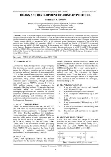
International Journal of Industrial Electronics and Electrical Engineering, ISSN: 2347-6982Special Issue, Sep.-2016DESIGN AND DEVELOPMENT OF ARINC 429 PROTOCOL1SMITHA M R, 2APARNA1M.Tech, VLSI design and embedded systems, Dept of ECE, 2Engineer, MCSRDC1Sapthagiri College of engineering Bangalore, INDIA,2Hindustan Aeronautics Limited, Bangalore, INDIAE-mail: 1smithamr01@gmail.com, 2acinthalkar@gmail.comAbstract – ARINC is the major company that develops and operates systems and services to ensure the efficiency, operationand performance of aviation and travel industries. ARINC 429 specification defines how the avionics equipment and systemsshould communicate with each other. It employs a unidirectional data bus standard known as Mark 33 Digital InformationTransfer Systems. ARINC 429 bus operates at 12.5 or 100 kilobits per second. The top level architecture of the ARINC 429protocol has 4 modules ARINC 429 transmitter, ARINC 429 receiver, Transmit and Receive 512*32-bit FIFO to store andfetch the data and ARINC 429 clock generation. In this proposed work ARINC 429 protocol is designed and developedusing Hardware Descriptive Language (HDL). The continuous data stream is stored in a 512*32-bit FIFO. The encodermodule at ARINC 429 transmitter converts a continuous data stream into Bipolar Return to Zero format. This encoded datais decoded at the receiver. The decoded data is stored in the ARINC 429 Receive FIFO. The design and development is doneusing Xilinx software.Keywords— ARINC 429, DITS, BPRZ encoding, FIFO, VHDLavionics systems on commercial aircraft. ARINC 429employs unidirectional data bus standard known asthe MARK 33 Digital Information Transfer System(DITS) specification. This is a very simple, point-topoint protocol. There can be only one transmitter on atwisted wire pair. The transmitter is alwaystransmitting either 32-bit data words or the NULLstate. The most messages consist of a single dataword. There is at least one receiver on a wire pair,there may be up to 20.I. INTRODUCTIONAeronautical Radio, Incorporated is a major companythat develops and operates systems and services toensure the efficiency, operation and performance ofthe aviation and travel industries. It was organized in1929 by four major airlines to provide a single licenseand initiator of radio communications outside thegovernment. Only airlines and aviation relatedcompanies can be shareholders, although all airlinesand aircraft can use ARINC’s services. It is now a 280 million company with headquarters inAnnapolis, Maryland and over 50 operating locationsworldwide. ARINC has provided leadership indeveloping specifications and standards for avionicsequipment and these specifications are used to definephysical packaging and mounting of avionicsequipment, data communications standards and Highlevel computer languages.C. FEATURES OF ARINC 429i.It has selectable data rates on each channelas 12.5kbps or 100 kbpsii.It provides direct cpu access to memory.iii.It has configurable label memory up to 256words.iv.It has selectable clock speed of 1, 10, 16 or20 Mhz.v.It has programmable FIFO depth up to 512words.vi.It uses Bi-polar return to zero encoding anddecoding methods.vii.Transmission and reception is on separateports.A. ARINC STANDARD SERIESARINC has number of series like 400, 500, 600, 700and each series has its own advantages and used fordifferent avionics equipment’s. For example ARINC400 Series describes guidelines for installation,wiring, data buses and databases. ARINC 500 Seriesdescribes older analog avionics equipment used onearly jet aircraft such as the Boeing 727, DouglasDC-9, DC-10, Boeing 737, 747 and Airbus A300.ARINC 600 is the predominant avionics packagingstandard introducing the avionics Modular ConceptUnit. ARINC 700 series describes the form, fit ly on transport category aircraft.D. ARINC 429 WORD FORMATARINC 429 data words are always 32 bits andtypically use the format shown in Figure.1 whichincludes five primary fields namely Parity, SSM,Data, SDI, and Label. ARINC 429 conventionnumbers the bits from 1 (LSB) to 32 (MSB).B. ARINC 429ARINC 429 specification defines the standardrequirements for the transfer of digital data betweenFigure 1: Generalised ARINC 429 word formatDesign and Development of ARINC 429 Protocol6
International Journal of Industrial Electronics and Electrical Engineering, ISSN: 2347-6982 Transmission orderThe order of the bits transmitted on the ARINC 429bus is as follows: 8, 7, 6, 5, 4, 3, 2, 1, 9, 10, 11, 12, 13 32. Here the least significant bit of each byte,except the label is transmitted first and the label istransmitted ahead of the data in each case.Special Issue, Sep.-2016 HI this should measure between 7.25 and 11volts between the two wires (A to B). NULL this should be between 0.5to -0.5 (Ato B). LO this should be between -7.25 to-11 volts(A to B).The received voltage depends on line length andthe number of receivers connected to the bus. Nomore than 20 receivers should be connected to asingle bus and no less than one receiver. Since eachbus is unidirectional, a system needs to have its owntransmit bus if it is required to respond or to sendmessages. The transmitting and receiving circuitsmust be designed for reliably sending and detectingthe null transition between high and low states. ParityThe MSB 32 is always the parity bit for ARINC 429.Parity is normally set to odd except for certain tests.Odd parity means that there must be an odd numberof 1 bits in the 32-bit word that is insured by eithersetting or clearing the parity bit. SSMBits 31 and 30 contain the Sign/Status Matrix. Thisfield contains hardware equipment condition,operational mode or validity of data content. DataBits 29 through 11 contain data which may be in anumber of different formats. There are also manynon-standard formats that have been implemented byvarious manufacturers. In some cases, the data fieldoverlaps down into the SDI bits. In this case, the SDIfield is not used. SDIBits 10 and 9 provide a Source/Destination Identifier.This is used for multiple receivers to identify thereceiver for which the data is destined. It can also beused in the case of multiple systems to identify thesource of the transmission. In some cases, these bitsare used for data. ARINC 429 can have only onetransmitter on a pair of wires, but up to 20 receivers.Figure 2: ARINC 429 Bipolar Return to zero formatA. FIRST PHASE OF ARINC 429The core consists of three main blocks:Transmit, Receive and CPU Interface. Core 429requires connection to an external CPU. The CPUinterface configures transmit and receive controlregisters and initializes the label memory. The coreinterfaces to the ARINC 429 bus through an externalARINC 429 line driver and line receiver as shown infigure 3. LabelBits 8 through 1 contain a label identifying the datatype and the parameters associated with it. The labelis an important part of the message. It is used todetermine the data type of the remainder of the wordand therefore the method of data translation to use.Labels are typically represented as octal numbers.II. OPERATIONS OF ARINC 429An ARINC 429 data bus uses two signal wires totransmit 32 bit words. Transmission of sequentialwords is separated by at least 4 bit times of NULL(zero voltage). This eliminates the need for a separateclock signal wire. That’s why this signal is known asa self-clocking signal. The nominal transmissionvoltage is 10 1 volts between wires (differential),with either a positive or negative polarity. Therefore,each signal leg ranges between 5V and -5V. If oneleg is 5V the other is -5V and vice-versa. One wireis called the “A” (or “ ” or “HI”) side and the other isthe “B” (or “-” or “LO”) side. This is known asbipolar return-to zero (BPRZ) modulation as shownin figure 2. The composite signal state may be one ofthree levels:Figure 3: Typical core systemCore 429 provides a complete and flexibleinterface to a microprocessor and an ARINC 429 databus. Connection to an ARINC 429 data bus requiresadditional line drivers and line receivers. Core 429interfaces to a processor through the internal memoryof the receiver. Core 429 can be easily interfaced toan 8, 16 or 32-bit data bus. Look-up tables loadedinto memory enable the Core 429 receive circuitry toDesign and Development of ARINC 429 Protocol7
International Journal of Industrial Electronics and Electrical Engineering, ISSN: 2347-6982filter and sort incoming data by label and destinationbits. Core 429 supports multiple ARINC 429 receiverchannels and each receives data independently. Thereceiver data rates (high or low speed) can beprogrammed independently. Core429 can decode andsort data based on the ARINC 429 Label and SDI bitsand stores it in FIFO. Each receiver usesprogrammable FIFO to buffer received data.Special Issue, Sep.-2016A. LOOPBACK TESTIn loopback test the input data is taken fromHOST and the input data is stored in 512*32 transmitFIFO as 32-bit data.B. SECOND PHASE OF ARINC 429The Transmitter module converts the 32-bit paralleldata from the TX FIFO to serial data. It also insertsthe parity bit into the ARINC 429 data when parity isenabled. The CPU interface is used to fill the FIFOwith ARINC 429 data. The TX FIFO can hold up to512 ARINC 429 words of data. The transmissionstarts as soon as one complete ARINC 429 word hasbeen stored in the transmit FIFO. The TX modulecontains two 8-bit registers. One is used for a controlfunction and the other is used for status. The CPUinterface allows the system CPU to access the controland status registers within the core. Depending on theTXFIFO status signals, the CPU will either read theTXFIFO before it overflows or not attempt to readthe TXFIFO if it is empty.Figure 4: Block diagram of ARINC 429 with loopback testB. INDIVIDUAL TESTThe individual test of ARINC 429 consists ofTransmitter test and Receiver test.The ARINC 429 transmitter consists of four blocks:Transmit FIFO with the depth of 512 words, Parallelto serial register to convert the 32-bit data to a singlebit for encoding, BPRZ encoder which encodes theserial data into waveform, clock generation whichgenerates a 200 KHz. Transmit FIFO takes the inputfrom a host as shown in figure 5.C. FINAL PHASE OF ARINC 429The Receiver block is responsible for recovering theclock from the input serial data and performs serialto-parallel conversion and gap/parity check on theincoming data. It also interfaces with the CPU. TheRx module contains two 8-bit registers. One is usedfor control function and the other is used for status.The CPU interface configures the internal RAM withthe labels, which are used to compare against theincoming labels from the received ARINC 429 data.If the label-compare bit in the receive control registeris enabled, then the data which matches its labels withthe stored labels will be stored in the RXFIFO. If thelabel compare bit in the receive control register isdisabled, then the incoming data will be stored in theRXFIFO without comparing against the labels inRAM. The core supports reloading label memoryusing bit 7 of the Rx control register. Depending onthe RXFIFO status signals, the CPU will either readthe RXFIFO before it overflows or not attempt toread the RXFIFO if it is empty.Figure 5: Block diagram of ARINC 429 TransmittertestThe ARINC 429 receiver consists of BPRZ decoder,32-bit shift register and 512*32 bit RXFIFO. TheDATA APLUS and DATA AMINUS are theARINC 429 transmitted data which is the input to thedecoder. The clock is recovered and the BPRZdecoder recovers the original data. The recovereddata is sent as a 32- bit parallel data to receive FIFO.The data from the receive FIFO is read by the host asshown in figure 6.III. TESTING METHODOLOGY OF ARINC 429There are two types of testing ARINC 429 protocolsuch as loopback test and individual test.This 32-bit data is encoded in Bi-polar Return to zeroformat. The encoded data is transmitted by ARINC429 encoder and transmit it to the receiver. TheARINC 429 decoder decodes the data and stores thedata in 512*32 receive FIFO. The data from thereceive FIFO is looped back to the interface betweeninput data and transmit FIFO to check if the datareceived is same as transmitted data.Figure 6: Block diagram of ARINC 429 Receiver testDesign and Development of ARINC 429 Protocol8
International Journal of Industrial Electronics and Electrical Engineering, ISSN: 2347-6982IV. IMPLEMENTATION OF ARINC 429A. Top level block diagram of ARINC 429The top level block diagram of ARINC 429 is asshown in Figure 7. The ARINC test bench providesthe input data to the ARINC 429 module. It acts as amicrocontroller. The test bench inputs are theaddresses and data. The ARINC clock generationtakes the clock provided by the microcontroller100/50 MHz in this case and generates a ARINC 429clock of 200 KHz which is used by the transmitterand the receiver.Special Issue, Sep.-2016B. Top level Finite State Machine for ARINC 429IP coreThe Finite State Machine for ARINC 429 is asshown in the Figure 8. There are five states: Resetstate, idle state (s1), configuration state, transmitstate, and receive state. The events for the FSM arereset, config, START TX, STOP TX, START RX,STOP RX.The working of the FSM is as stated below:When reset event occurs, reset state transitions to idlestate or to reset state itself depending upon the event.If reset is 1, the state transitions to itself or if reset is0, the state transitions to idle state. Whenconfiguration event is set to1 the state transits fromidle state to configuration state. The transition fromthe configuration state to transmit state or receivestate occurs depending on which of the eventoccurred. If START TX event had occurred, theconfiguration state transitions to transmit state, else ifSTART RX had occurred, the transition will be toreceive state. In transmit or receive state the configwill be set to 0. During no transmission or receptionof data the STOP TX or STOP RX eve
ARINC 429 specification defines how the avionics equipment and systems should communicate with each other. It employs a unidirectional data bus standard known as Mark 33 Digital Information Transfer Systems. ARINC 429 bus operates at 12.5 or 100 kilobits per second. The top level architecture of the ARINC 429 protocol has 4 modules ARINC 429 transmitter, ARINC 429 receiver, Transmit and .