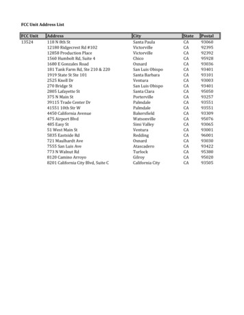
Transcription
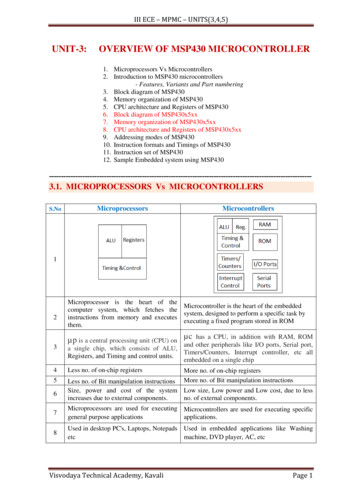
III ECE – MPMC – UNITS(3,4,5)UNIT-3:OVERVIEW OF MSP430 MICROCONTROLLER1. Microprocessors Vs Microcontrollers2. Introduction to MSP430 microcontrollers- Features, Variants and Part numbering3. Block diagram of MSP4304. Memory organization of MSP4305. CPU architecture and Registers of MSP4306. Block diagram of MSP430x5xx7. Memory organization of MSP430x5xx8. CPU architecture and Registers of MSP430x5xx9. Addressing modes of MSP43010. Instruction formats and Timings of MSP43011. Instruction set of MSP43012. Sample Embedded system using ----------------3.1. MICROPROCESSORS Vs s12Microprocessor is the heart of theMicrocontroller is the heart of the embeddedcomputer system, which fetches thesystem, designed to perform a specific task byinstructions from memory and executesexecuting a fixed program stored in ROMthem.3has a CPU, in addition with RAM, ROMµp is a central processing unit (CPU) on µcand other peripherals like I/O ports, Serial port,4Less no. of on-chip registers5Less no. of Bit manipulation instructionsSize, power and cost of the system Low size, Low power and Low cost, due to lessincreases due to external components.no. of external components.6a single chip, which consists of ALU,Timers/Counters, Interrupt controller, etc allRegisters, and Timing and control units.embedded on a single chipMore no. of on-chip registersMore no. of Bit manipulation instructions7Microprocessors are used for executing Microcontrollers are used for executing specificgeneral purpose applicationsapplications.8Used in desktop PC's, Laptops, Notepads Used in embedded applications like Washingetcmachine, DVD player, AC, etcVisvodaya Technical Academy, KavaliPage 1
III ECE – MPMC – UNITS(3,4,5)3.2. INTRODUCTION TO MSP430 FAMILYIntroduction to MSP430 : MSP430 family microcontrollers from Texas Instruments (TI), are designed for low cost,low power and portable embedded applicationsMSP430 has 16-bit RISC based processor architectureIt supports different Low power modesIt has 16 registers (R0-R15)All registers are 16-bit wideIt has 16-bit Address bus and 16-bit data busSupports 27 core instructions, 24 emulated instructions and 7 addressing modesIt is capable of wake-up time below 1 microsecondExtensive vectored-interrupt capabilityA wide range of on-chip peripherals are availableFeatures of MSP430 :Although there are variants in devices in the family, a MSP430 microcontroller can becharacterized by:Device parameters Flash/ ROM options: 1 KB – 60 KB RAM options: 128 B– 8 KB GPIO options: 14 - 80 pinsClock and Power Specifications CPU clock: 8/16/25 MHz Operating voltage: 1.8–3.6 V Active operation: 160 - 250 µA/MIPS RTC mode operation : 0.7 µA RAM retention: 0.1 μA Fast wake-up from standby mode in less than 1 µsOther integrated peripherals* Basic Clock system* I/O ports* Serial Port : SPI, I2C, UART* Timers* WDT (Watch Dog Timer )* RTC (Real Time Clock)* Multiplier* DMA* LCD driver* Supply Voltage Supervisor (SVS)* Brown out Reset* The emulator and JTAG interfaceVisvodaya Technical Academy, Kavali*****10/12/16-bit ADC12-bit dual DACOp-AmpComparator ATemp. sensorPage 2
III ECE – MPMC – UNITS(3,4,5)Advantages of MSP430 family : 16-bit RISC architectureHigh-performance - High speed of executionLow power consumptionFast wake-up from standby mode in less than 1 µsVariety of models with integrated memories, multiple programmable GPIO andIntegrated application-specific peripheralsCost-effectiveApplications of MSP430 Low power, hand-held smart devicesTest and measurement equipmentSmart Energy/Smart Grid solutionsFactory automationHome and commercial site monitoring and controlMedical instrumentationFire and securityIntelligent lighting controlTransportationMotion controlAutomobilesGaming equipmentVARIANTS OF MSP430 FAMILY(i) MSP430x1xx MSP430x1xx Provides a wide range of general-purpose devices from simple versions tocomplete systems for processing signals. There is a broad selection of peripherals and someinclude a hardware multiplier, which can be used as a basic digital signal processor. The integrated peripherals include - 12-bit DAC, two 16-bit timers, WDT, brown-out reset,SVS, USART module (UART, SPI), DMA, 16 16 multiplier, Comparator A, Temp.Sensor(ii) MSP430x2xx The MSP430F2xx Series are similar to the '1xx generation, but operate at even lowerpower, support up to 16 MHz operation, double the speed of earlier devices, whileconsuming only half the current at the same speed. It has On-chip clock (VLO) that makesit easier to operate without an external crystal. Pull-up or pull-down resistors are providedon the inputs to reduce the number of external components needed. The integrated peripherals include -operational amplifiers, 12-bit DAC, two 16-bit timers,watchdog timer, brown-out reset, SVS, USI module (I²C, SPI), USCI module, DMA,16 16 multiplier, Comparator A , Temperature sensor(iii) MSP430x3xx The MSP430x3xx Series is the oldest generation, designed for portable instrumentationwith an embedded LCD controller. This also includes a frequency-locked loop oscillatorthat can automatically synchronize to a low-speed (32 kHz) crystal.Visvodaya Technical Academy, KavaliPage 3
III ECE – MPMC – UNITS(3,4,5) This generation does not support EEPROM memory, only mask ROM and UV- eraseableand one-time programmable EPROM. The integrated peripherals include - LCD controllerand multiplier(iv) MSP430x4xx MSP430x4xx series can drive LCDs with up to 160 segments. Many of them are ASSPs,but there are general-purpose devices as well. These devices are used for low powermetering and medical applications. The integrated peripherals include - 12-bit DAC, Op Amps, RTC, up to two 16-bit timers,watchdog timer, basic timer, brown-out reset, SVS, USART module (UART, SPI), USCImodule, LCD Controller, DMA, 16 16 & 32x32 multiplier, Comparator A, Temp. sensor(v) MSP430x5xxThe MSP430x5xx Series are able to run up to 25 MHz, have up to 512 KB flash memoryand up to 66 KB RAM. It includes an innovative power management module for optimalpower consumption and integrated USB. The other integrated peripherals include - Highresolution PWM, 5 V I/O's, backup battery switch, up to 4 16-bit timers, watchdog timer,Real-Time Clock, brown-out reset, SVS, USCI module, DMA, 32x32 multiplier, Comp B,temperature sensorMSP430X : There is a new extended version of original MSP430 architecture, called MSP430X, whichcan address extra memory with other improvements as well. If CPU is MSP430, it has 16-bit address bus and it can address 64 KB of memory (0x0000– 0xFFFF). If the CPU is MSP430X, it has 20-bit address bus and it can address 1 MB ofmemory. The bottom 64 KB of memory from 0x0000 to 0xFFFF is same way as in theoriginal MSP430. The additional memory from 0x10000 to 0xFFFFF, is available foradditional ROM. This allows larger programs and tables to be stored.Variants ofMSP430 30x5xxClock8 MHz16 MHz16 MHz16 MHz16 MHzIactive /MIPS200 μA200 μA160 μA200 μA165 μAIRTC mode0.7 μA0.7 μA0.9 μA0.7 μA2.5 μAIRAMret0.1 μA0.1 μA0.1 μA0.1 μA0.1 μAWake-up time 6 µs 1 µs 6 µs 6 µs 5 µs1-60KB1-60KB2-32 KB4-60 KBup to 512KBRAM128 B -2KB128 B -2KB512 B -2KB256 B -2KBup to a Technical Academy, KavaliPage 4
III ECE – MPMC – UNITS(3,4,5)MSP430 PART NUMBERINGMSP 430FG(optional)The letters MSP stand for mixed signal processorMSP430 indicates the member of the 430 MCU platforms.The letter after MSP430 shows the type of memory.F : flash memory,C : masked ROMThere is a second letter for ASSPs to show the type of measurement forwhich they are intended.E : for electricity (Energy meters),W : for water (flow meters), andG : for signals that require gain stage provided byOp-Amps (Medical)4It indicates the generation of the device6Model within generation19Memory size and peripheral configurationIQZWR(optional)Temperature rangeI : -40 to 85 oCT : -40 to 105 oCS : 0 to 50 oCPackage : Ball Grid Array/ Pin Grid Array/ Dual In-lineTape and Reel :Visvodaya Technical Academy, KavaliT Small Reel (7 –in),R Large Reel (11 –in)Page 5
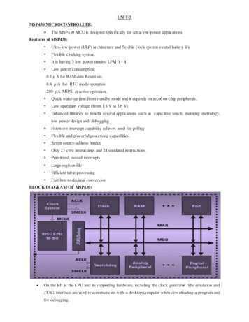
III ECE – MPMC – UNITS(3,4,5)3.3. BLOCK DIAGRAM OF MSP430 F2013 / F2003Introduction to MSP430 :MSP430 family microcontrollers from Texas Instruments (TI), are designed for low cost,low power and portable embedded applicationsMSP430 has 16-bit RISC based processor architectureIt supports different Low power modesIt has 16 registers : R0-R15All registers are 16-bit wideIt has 16-bit Address bus and 16-bit data busSupports 27 core instructions, 24 emulated instructions and 7 addressing modesIt is capable of wake-up time below 1 microsecondExtensive vectored-interrupt capabilityA wide range of on-chip peripherals are availableThe functional block diagram of the MSP430 F2003/F2013 is shown in figure. The main blocksare linked by the memory address bus (MAB) and memory data bus (MDB).Visvodaya Technical Academy, KavaliPage 6
III ECE – MPMC – UNITS(3,4,5)16-bit CPU : It consists of 16-bit ALU, set of 16-registers (R0 – R15) and Logic needed to decode andexecute the instructionsThe CPU has RISC architectureInstructions processing on either bits, bytes or wordsSupports 27 instructions and 7 addressing modes.It can address the complete address range without paging CPU clock: 16 MHz Operating voltage: 1.8–3.6 V Active operation: 200 µA/MIPS RTC mode operation : 0.7 µA RAM retention: 0.1 μA Fast wake-up from standby mode in less than 1 µsBasic Clock system :The clock module provides the CLK for CPU and peripherals. Three clock signals areavailable from the basic clock module:MCLK: Master clock is used by CPU and systemSMCLK: Subsystem Master clock is distributed to high speed peripheralsACLK: Auxiliary clock is also distributed to low speed peripheralsThe emulator and JTAG interfaceThe emulation, JTAG interface and Spy-Bi-Wire are used to communicate with a desktopcomputer when downloading a program and for debugging.Flash memoryFlash memory is used to store the programs and constant variablesThe size of Flash memory in MSP430F2003 is 1 KBThe size of Flash memory in MSP430F2003 is 2 KBRAMRAM is used to store the temporary data (Read/Write memory)The size of RAM in MSP430F2003 and F2013 is 128 Bytes16-bit Sigma Delta ADC : SD16 AThe SD16 A is ahigh performance 16-bit analog to digital converterused to interface analog signals with 200 KSPSI/O ports : P1 & P2The MSP430 has Two I/O ports: Port-P1 and Port-P2The Port-P1 has 8- I/O pins and P2 has 2- I/O pinsEach I/O pin is individually configurable for input (or) output.Each pin can be configurable for pull-up / pull-down resistorsPorts P1 and P2 have interrupt capability.Visvodaya Technical Academy, KavaliPage 7
III ECE – MPMC – UNITS(3,4,5)Watch Dog Timer A watchdog timer (WDT) is an electronic timer that is used to detect and recover fromcomputer malfunctions. The WDT module restarts the system on occurrence of a softwareproblem (or) if a selected time interval expires.During normal operation, the system regularly restarts the WDT to prevent it from elapsing,or "timing out". If the system fails to restart the WDT due to a hardware fault (or) programerror, the timer will elapse and generate a timeout signal.The timeout signal is used to initiate corrective actions like placing the system in a safestate and restoring normal system operation.Timer A2 Timers are essential to almost any embedded applicationTimers are used to- Generate fixed-period events- Periodic wakeup- Count edges- Generate delays- Measure time intervals- Replacing delay loops with timer calls allows CPU to sleep, consuming less powerTimers can support multiple capture/compares, PWM outputs, interval timing and extensiveinterrupt capabilitiesUniversal Serial Interface (USI) :The Universal Serial Interface (USI) module supports multiple serial communication modesUART : Asynchronous, Full duplexSPI: Serial Peripheral Interface - Synchronous, Full duplexI2C: Serial Peripheral Interface -Synchronous, Half duplexBrown out Reset The brownout protection comes into action if the supply voltage drops to a dangerous levelThe brownout reset circuit detects low supply voltages such as when a supply voltage isapplied to (or) removed from the VCC terminal. The brownout reset circuit resets thedevice by triggering a POR (Power on Reset) signal when power is applied (or) removed.The brownout circuit is used to provide the proper internal reset signal to the device duringpower ON and power OFF. The Supply Voltage Supervisor (SVS) is used to monitor the supply voltage or an externalvoltage. The SVS can be configured to set a flag or generate a POR reset when the supplyvoltage or external voltage drops below a user selected threshold.Visvodaya Technical Academy, KavaliPage 8
III ECE – MPMC – UNITS(3,4,5)3.4. ADDRESS SPACE / MEMORY MAPPING OF MSP430 The MSP430 has Von-Neumann architecture, in which the address space is shared with specialfunction registers (SFRs), peripherals, RAM, and Flash/ROM memory.The following shows the memory map of the F2013. Most MSP430 devices have a similarmemory map, differing only in the size of the regions for RAM and ROM.The data is stored in memory as Little-endian ordering, in which the low -byte of data isstored at lower memory address and high-byte of data is stored at the higher address.Figure : Memory map of the MSP430F20130000 – 000FSpecial Function Registers (byte access)0010 – 00FFPeripheral registers with Byte access0100 – 01FFPeripheral registers with Word access0200 – xxxxRAM ( upper boundary varies)0C00 – 0FFFBootstrap loader ( not in F20xx)1000 – 10FFFlash Information memory( available in Flash devices only)xxxx - FFBFFlash / ROM ( lower boundary varies)FFC0 - FFFFInterrupt Vector TableVisvodaya Technical Academy, KavaliPage 9
III E
Instruction set of MSP430 12. Sample Embedded system using MSP430 ----- 3.1. MICROPROCESSORS Vs MICROCONTROLLERS S.No Microprocessors Microcontrollers 1 2 Microprocessor is the heart of the computer system, which fetches the