Transcription
RFoundations and Trends inElectronic Design AutomationVol. 6, No. 2 (2012) 121–216c 2012 S. Reda and A. N. Nowroz DOI: 10.1561/1000000022Power Modeling and Characterization ofComputing Devices: A SurveyBy Sherief Reda and Abdullah N. NowrozContents1 Introduction1231.11.21.3126131133Computing SubstratesSurvey OverviewSummary2 Background: Basics of Power Modeling1342.12.22.3135140144Dynamic PowerStatic PowerSummary3 Pre-Silicon Power Modeling Techniques1463.13.23.33.4147160167173Power Modeling for General-Purpose ProcessorsPower Modeling for SoC-Based Embedded SystemsPower Modeling for FPGAsSummary
4 Post-Silicon Power Characterization1754.14.21764.34.4Power Characterization for Validation and DebuggingPower Characterization for AdaptivePower-Aware ComputingPower Characterization for Software Power AnalysisSummary1851891965 Future Directions199Acknowledgments203Notations and Acronyms204References207
RFoundations and Trends inElectronic Design AutomationVol. 6, No. 2 (2012) 121–216c 2012 S. Reda and A. N. Nowroz DOI: 10.1561/1000000022Power Modeling and Characterization ofComputing Devices: A SurveySherief Reda1 and Abdullah N. Nowroz212Brown University, 182 Hope st, Providence 02912, USA,sherief reda@brown.eduBrown University, 182 Hope st, Providence 02912, USA,Abdullah nowroz@brown.eduAbstractIn this survey we describe the main research directions in pre-siliconpower modeling and post-silicon power characterization. We reviewtechniques in power modeling and characterization for three computingsubstrates: general-purpose processors, system-on-chip-based embedded systems, and field programmable gate arrays. We describe the basicprinciples that govern power consumption in digital circuits, and utilizethese principles to describe high-level power modeling techniques fordesigns of the three computing substrates. Once a computing deviceis fabricated, direct measurements on the actual device reveal a greatwealth of information about the device’s power consumption undervarious operating conditions. We describe characterization techniquesthat integrate infrared imaging with electric current measurements togenerate runtime power maps. The power maps can be used to validate design-time power models and to calibrate computer-aided design
tools. We also describe empirical power characterization techniquesfor software power analysis and for adaptive power-aware computing.Finally, we provide a number of plausible future research directions forpower modeling and characterization.
1IntroductionIn the past decade power has emerged as a major challenge tocomputing advancement. A recent report by the National ResearchCouncil (NRC) of the National Academies highlights power as thenumber one challenge to sustain historical improvements in computing performance [39]. Power is limiting the performance of both mobileand server computing devices. At one extreme, embedded and portablecomputing devices operate within power constraints to prolong batteryoperation. The power budgets of these devices are about tens of milliWatts for some embedded systems (e.g., sensor nodes), 1–2 W formobile smart phones and tablets, and 15–30 W for laptop computers.At another extreme, high-end server processors, where performance isthe main objective, are increasingly becoming hot-spot limited [46],where increases in performance are constrained by a maximum junction temperature (typically 85 C). Economic air-based cooling techniques limit the total power consumption of server processors to about100–150 W, and it is the spatial and temporal allocation of the powerdistribution that leads to hot spots in the die that can comprise thereliability of the device. Because server-based systems are typicallydeployed in data centers, their aggregate performance becomes power123
124Introductionlimited [6], where energy costs represent the major portion of total costof ownership. The emergence of power as a major constraint has forceddesigners to carefully evaluate every architectural and design featurewith respect to its performance and power trade-offs. This evaluationrequires pre-silicon power modeling tools that can navigate the richdesign landscape. Furthermore, runtime constraints on power consumption require power management tools that control a number of runtimeknobs that trade-off performance and power consumption. Power management techniques that seek to meet a power cap, e.g., as in the case ofservers in data centers [6, 37], require either direct power measurementswhen feasible, or alternatively, runtime power modeling techniques thatcan substitute direct characterization. In addition, software power characterization can help tune and restructure algorithms to reduce theirpower consumption.The last decade has seen a diversification in possible computing substrates that offer different trade-offs in performance, power, and costfor different applications. These substrates include application-specificcustom-fabricated circuits, application-specific circuits implemented infield-programmable logic arrays (FPGAs), general-purpose processorswhose functionality is determined by software, general-purpose graphical processing units (GP-GPUs), digital signal processors (DSPs), andsystem-on-chip (SoC) substrates that combine general-purpose coreswith heterogeneous application-specific custom circuits. None of thesesubstrates necessarily dominate the other, but they rather offer certainadvantages that depend on the target application and the deploymentsetting of the computing device. For instance, custom fabricated circuits outperform their FPGA counterparts in performance and power,but they are more expensive. SoCs offer higher performance/Watt ratiofor a range of applications than general-purpose processors; however,general-purpose processors offer higher throughput for scientific applications. GPGPUs are also emerging as a strong contender to processorsand FPGAs; however, the relative advantage of each of these substratesdiffers by the application [39, 54, 76]. Sorting out the exact trade-offsof all these substrates across different application domains is an activearea of research [4, 29, 76]. While power modeling and characterizationfor these substrates share common concepts, each of these substrates
125has its own peculiarities. In this survey we will discuss the basic powermodeling and characterization concepts that are shared among thesesubstrates as well as the specific techniques that are applicable foreach one.Pre-silicon power modeling and post-silicon power characterizationare very challenging tasks. The following factors contribute to thesechallenges.(1) Large die areas with billions of transistors and interconnectslead to computational difficulties in modeling.(2) Input patterns and runtime software applications triggerlarge variation in power consumption. These variations arecomputationally impossible to enumerate exhaustively during modeling.(3) Spatial and temporal thermal variations arising from powerconsumption trigger large variations in leakage power, whichlead to intricate dependencies in power modeling.(4) Process variabilities that arise during fabrication lead tointra-die and inter-die power leakage variations that areunique to each die. These deviations recast the modelingresults to be educated guesses, rather than exact estimates.(5) Practical limitations on the design of power-delivery networks make it difficult to directly characterize the runtimepower consumption of individual circuit blocks.The objective of this survey is to describe modern researchdirections for pre-silicon power modeling and post-silicon powercharacterization. Pre-silicon power modeling tools estimate the powerconsumption of an input design, and they can be used to create apower-aware design exploration framework, where different designchoices are evaluated in terms of their power impact in addition totraditional design objective such as performance and area. Post-siliconpower characterization tools are applied to a fabricated design tocharacterize its power consumption under various workloads andenvironmental variabilities. The results of power characterization areuseful for power-related debugging issues, calibration of design-timepower modeling tools, software-driven power analysis, and adaptive
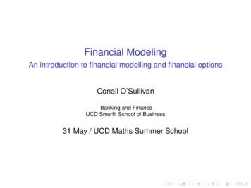
126Introductionpower-aware computing. Our technical exposition reviews power modeling and characterization techniques of various computing substrates,while emphasizing cross-cutting issues. We also connect the dotsbetween the research results of different research communities, such ascircuit designers, computer-aided design (CAD) developers, computerarchitects, and system designers. Our discussions reveal the sharedconcepts and the different research angles that have been explored forpower modeling and characterization.1.11.1.1Computing SubstratesGeneral-Purpose ProcessorsA general-purpose processor is designed to serve a large variety of applications, rather than being highly tailored to one specific application ora class of applications. The design of a general-purpose processor hasto be done carefully to lead to good performance within the processor’s thermal design power (TDP) limit under different kinds of workloads. The TDP limit has forced a significant change in the design ofprocessors. At present, designers aim to increase the processor’s totalthroughput rather than improving the single-thread performance. Thisthroughput increase is achieved by using more than one processing coreper chip.Figure 1.1 gives an example of a quad-core processor based on Intel’sCore i7 Nehalem architecture. The 64-bit processor features four coresthat share an 8 MB of L3 cache. The cores can run up to 3.46 GHz in a130 W TDP. Each core has a 16-stage pipeline and includes a 32 KB L1instruction cache, a 32 KB L1 data cache, and a 256 KB of L2 cache.The front-end of the pipeline can fetch up to 16 bytes from the L1instruction cache. The instructions in the fetched 16 bytes are identified and inserted into an instruction queue. The decoder unit receives itsinputs from the instruction queue, and it can decode up to four instructions per cycle into micro-ops. A branch prediction unit with a branchtarget buffer enables the core to fetch and process instructions beforethe outcome of a branch is determined. The back-end of the pipelineallocates resources for the micro-ops and renames their source and destination registers to eliminate hazards and to expose instruction-level
1.1 Computing Substrates127Core 1Core 2Core 3 Core 4DecodeRename/ AllocateRetirement UnitReorder BufferShared L3 CacheSchedulersReservation StationsExecution EngineOut-of-OrderInstruction QueueFront-EndIn-OrderInstruction Fetch and PreDecodeExecution UnitsL2 D-Cache (256KB)MemoryL1 D-Cache (32KB) and D-TLBShared L3 Cache (8 MB)Fig. 1.1. High-level diagram of Intel Core i7 processor (Nehalem architecture).parallelism. The micro-ops are then queued in the re-order buffer untilthey are ready for execution. The pipeline can dynamically scheduleand issue up to six micro-ops per cycle to the execution units as longas the operands and resources are available. The execution units perform loads, stores, scalar integer or floating-point arithmetic, and vectorinteger or floating-point arithmetic. The results from the execution ofmicro-ops are stored in the re-order buffer, and results are committedin-order only for correct instruction execution paths.1.1.2Embedded SoCSoCs are computational substrates that are targeted for embeddedsystems and mobile computing platforms for a certain niche of applications. An SoC for a smart phone or a tablet typically consumes lessthan 1–2 W of power, while delivering the throughput required for
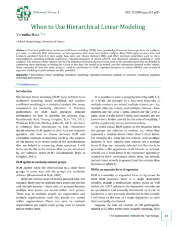
128Introductionapplications that include video and audio playback, internet connectivity, and games. In contrast to a general-purpose processor, an SoCincludes, in addition to the general-purpose core(s), application-specificcustom hardware (HW) components that can provide the requiredthroughput for the target applications within the power envelope ofthe embedded system. Because total die area is constrained by costand yield considerations, the inclusion of application-specific customHW components must come at the expense of the functionality ofthe general-purpose core. SoC general-purpose cores are less capablethan the ones used in general-purpose processors. They are usually lessaggressively pipelined with limited instruction-level parallelism capabilities and smaller cache sizes.Figure 1.2 gives an example of an SoC based on nVidia’s Tegraplatform that has a total power budget of about 250 mW. The SoC features a 32-bit ARM11 general-purpose core that runs up to 800 MHz.The ARM11 core has an 8-stage pipeline, with a single instruction issueand support for out-of-order completion. The L1 data and code cachememory sizes are 32 KB each, and the size of the L2 cache is 256 KB.The performance specifications of the core are clearly inferior comparedto the specifications of the Core i7. To compensate for the lost generalpurpose computing performance, the SoC uses a number of applicationspecific components to deliver the required performance within itsFig. 1.2. Example of nVidia Tegra SoC.
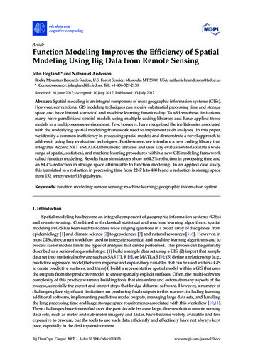
1.1 Computing Substrates129power budget. These include an image signal processor that can provideimage processing functions (e.g., de-noising, sharpening, and color correction) for images captured from embedded cameras. The SoC includesa high-definition audio and video processor for image, video and audioplayback, and a GPU to deliver the required graphics performancefor 3-D games. The SoC supports an integrated memory controller,an encryption/decryption accelerator component, and components forcommunication, such as Universal Asynchronous Receiver/Transmitter(UART), Universal Serial Bus (USB), and High-Definition MultimediaInterface (HDMI). All SoC components communicate with each otherusing an on-chip communication network, which can take a number offorms, including shared and hierarchical busses, point-to-point busses,and meshes.1.1.3Field-Programmable Gate ArraysSoaring costs associated with fabricating computing circuitry atadvanced technology nodes have increased the interest in programmable logic devices that can be configured after fabrication to implementuser designs. The most versatile programmable logic currently availableis Field Programmable Gate Arrays (FPGAs). The basic FPGA architecture is an island-style structure, where programmable logic arrayblocks (LABs) are embedded in a reconfigurable wiring fabric that consists of wires and switch blocks as illustrated in Figure 1.3. The inputsand outputs of the LABs are connected to the routing fabric throughprogrammable switches. When programmed, these switches determinethe exact input and output connections of the LABs. In addition,10s–100s of programmable I/O pads are available in the FPGA. Inmany occasions, FPGAs also host heterogeneous dedicated computingresources, such as digital signal processors to implement multiplications, memory blocks to store runtime data, and even full light-weightprocessor cores.Each LAB is composed of several basic logic elements (BLEs), wherea BLE is made up of a 4-, 5-, or 6-input look-up table (LUT) togetherwith an associated flip-flop. A 4-input LUT can be used to implementany 4-input Boolean function. Figure 1.4(a) illustrates the structure
130IntroductionI/O padLogic ArrayBlockSwitchBlockWireSegmentFig. 1.3. Island-style FPGA.InputsOutK-inputLUTDFFClockBasic Logic Element (BLE)BLEOutputsBLEInputsLogic Array Block (LAB)Fig. 1.4. Typical design of a Logic Array Block (LAB) and a basic logic element (BLE).of a BLE and, Figure 1.4(b) illustrates the structure of a LAB. EachBLE can receive its inputs from other BLEs inside its LAB or fromother LABs through the reconfigurable wiring fabric. Additional wiringstructures in the LAB enable it to propagate arithmetic carry outputs
1.2 Survey Overview131in a fast and efficient way. To implement a computing circuit into anFPGA, it is first necessary to synthesize the input circuit by breaking itup into subcircuits, where each subcircuit is mapped to a BLE. TheseBLEs are then clustered into groups, where the size of each groupis determined by the number of BLEs in a LAB. These clusters arethen mapped and placed at the LABs. Finally, routing is conducted todetermine the exact routes and switches of the routing fabric used bythe circuit. The configuration bits for the logic and routing are storedin SRAM or FLASH memory cells.While FPGAs are very attractive to computer-system designers dueto their post-silicon flexibility, this flexibility comes at the expense ofhigher design area and power consumption compared to custom circuits that perform the same computing tasks. For example, Kuon andRose report almost a 35 overhead for using programmable logic overcustom logic [68]. However, for low to mid-volume fabrication, programmable logic is the only economically feasible technology. Alongwith performance and area, power is also an important factor thatmust be considered during architectural design exploration of FPGAs.FPGA architectural parameters include segment length, switch blocktopology, cluster size, BLE/LAB designs. Choices for these parameters lead to different power, performance, and area trade-offs. Thus,proper evaluation of power consumption is required to help designersand users make correct choices for the FPGA’s architecture and programmed designs.1.2Survey OverviewThe basic techniques for circuit-level power modeling are discussed inSection 2. The power consumption of computing circuits can be described by two components: dynamic power and static power. The sectionincludes discussions on how to estimate each of these components whenthe design’s circuit is available. We will also discuss the various factorsthat impact these power components, which include, circuit design andlayout, input patterns, fabrication technology, process variability, andoperational temperature. The discussions in Section 2 will form the basisfor the techniques discussed in Sections 3 and 4.
132IntroductionIn Section 3 we discuss techniques for pre-silicon power modeling techniques. Historically, performance and area were the two maincriteria during the design of computing devices. In the past 10–15 years,power has emerged as a third criterion that has to be considered during design. Every architectural feature has to be judged in terms of itsperformance, area and power. A typical design space has an exponential number of possible combination of settings for the various features.Thus, there is a strong need for power modeling methods that enabledesigners to efficiently explore the design space and to evaluate theimpact of various high-level system architectural choices and optimizations on power consumption. These architectural features and choicesvary by the medium of the computing substrate. For multi-core processors, the choices include, for example, pipeline depth, instruction issuewidth, and cache sizes. For SoC-based embedded systems, the choicesinclude, the functionality of the custom blocks and the on-chip communication architecture (e.g., network topology, buffer sizes and transfermodes). In some embedded systems, the boundary between hardware(HW) and software (SW) is fluid, where the choice of the implementation (SW or HW) of every component could be decided based on itsimpact on performance, power, and area. In embedded design environments, it is necessary to have power co-modeling tools that can effectively explore the possible HW/SW implementation choices of everydesign component, and guide designers to the correct choice. FPGApower modeling is also challenging as the user’s design is not knownduring the design and fabrication of the FPGA. Furthermore, users donot have direct access to the internal circuits of the FPGA. Thus, precharacterized power models for the different FPGA structures must beestimated during the design of the FPGA and then bundled with thevendor’s tools to be used by the end user.Once a design is implemented and a physical prototype is available for direct measurements, new opportunities become possible. InSection 4, we discuss a number of techniques for post-silicon powercharacterization. We describe techniques that integrate infrared imaging and direct electric current measurements to develop power mappingtechniques, that reveal the true power consumption of every designstructure. These true power maps can be used to validate pre-silicon
1.3 Summary133design estimates, to calibrate power-modeling CAD tools, and to estimate the impact of variabilities introduced during fabrication. We alsodiscuss power characterization techniques for adaptive power-awarecomputing, where power models based on lumped power measurementsare used by power management systems to cut down operational margins and to enforce runtime power constraints. Another discussed topicis SW power characterization using instruction-level, architectural-leveland algorithmic-level power models. SW power characterization helpssoftware developers and compiler designers to cut down the power consumption of their applications.1.3SummaryIn this section we have highlighted the importance of power modelingand characterization techniques for modern computing devices. Futurecomputing systems will be constrained by power, and the choices fordesign features and runtime settings have to be guided by the impacton power consumption as well as traditional objectives such as performance and implementation area.Computing substrates can come in a number of forms, includingcustom circuits with fixed functionality, general-purpose processorswhose functionality is determined by software applications, SoCs thatcombine general-purpose processing cores with application specific custom circuits, and programmable logic that can be used to implementcomputing circuits in a cost-effective way. These computing forms sharesome basic power modeling techniques; however, their unique architectural features enable them to utilize efficient large-scale modeling andcharacterization methods.Pre-silicon power modeling and post-silicon characterization techniques will be discussed in the remaining sections of this survey.The basic circuit-level power modeling techniques are discussed inSection 2. High-level power modeling techniques for various computingsubstrates will be discussed in Section 3. In Section 4 we overview different techniques for post-silicon power characterization through physical measurements on a fabricated device. Finally, a number of futureresearch directions are outlined in Section 5.
2Background: Basics of Power ModelingBasic transistor and circuit-level power modeling is a mature area ofresearch with numerous existing textbooks and surveys [73, 86, 99, 100].The objective of this section is to introduce sufficient background tounderstand the focus of this survey, which spans from pre-silicon highlevel power modeling techniques to post-silicon power characterizationtechniques. Power consumption of digital Complementary Metal OxideSemiconductor (CMOS) circuits is caused by two mechanisms. The firstmechanism is dynamic power, which arises when signals transition theirvalues, and the second mechanism is static power, which causes circuitsto dissipate power when no switching activity is occurring. One of themain advantages of using CMOS technology over earlier bipolar technology was that CMOS circuits consumed power only during circuitswitching. However, aggressive technology scaling in the past decadeled to a situation where static power is no longer negligible, but rathera significant contributor to total power consumption. This section discusses the basic principles and main challenges of circuit-level powermodeling. The techniques discussed in this section provide the basicbackground required for the next two sections.134
2.1 Dynamic Power2.1135Dynamic PowerLogic gates implemented in CMOS chips use two complementary transistor types, NMOS and PMOS, to build the functionality of each gate.One terminal of PMOS transistors is typically connected to the voltagesupply, VDD , while one terminal of NMOS transistors is connected tothe ground voltage VGND . Figure 2.1 gives the schematic of an invertergate that consists of one NMOS transistor and one PMOS transistor.To understand the operation of the gate, assume that the input voltage is first at logic 0 (i.e., VGND ). In this case the PMOS transistoris in on state with a very low resistance (ideally 0), while the NMOStransistor is in off state with a very high resistance (ideally ), and apath exists to charge the load capacitance CL until the output voltagereaches VDD . The load capacitance, CL , represents the total capacitancearising from the output diffusion capacitances of the two transistors, theinput capacitances of fan-out gates, wiring capacitance, and parasitics.When the input voltage switches to a logic 1 (i.e., VDD ), the PMOStransistor is in off state with a very high resistance (ideally ), whilethe NMOS transistor is in on state with a very low resistance (ideally 0),and a path exists to discharge the charges on the load capacitance tothe ground until the output voltage reaches 0. The sum of energy consumed during the charging and discharging, i.e., the energy per cycle, isVDDPMOSinputoutputCLNMOSGNDFig. 2.1. CMOS inverter.
136Background: Basics of Power Modeling2 . The dynamic power consumed, which is the switchingequal to CL VDDenergy per second, by the gate is equal to2,Pdynamic–gate sCL VDD(2.1)where s is an activity factor that denotes the number of switching cyclesper second. If a circuit has N gates, then the total dynamic power isequal toPdynamic N 2si CLi VDD,(2.2)iwhere si and CLi are the switching activity and load capacitance ofgate i respectively. Besides directly contributing to dynamic power,the capacitances also determine the exact propagation delays of thesignals, which influence the occurrence of signal glitches. Glitches areunnecessary signal transitions arising from unbalanced path delays atgate inputs as illustrated in Figure 2.2. In synchronous logic circuits, theclock signal has the highest switching activity, f , in the circuit. Thus,the buffer gates along the clock network path will have the highesttransition frequency. All other gates in the design can switch at a ratethat is at most half of f . Determining the exact switching activity ofeach gate is a challenging task because (1) it requires knowledge ofthe exact sequence of applied input vectors to the circuit; and (2) theexact signal timing information which is not accurately available untilthe final circuit layout is determined. The final layout provides theexact wiring and parasitic capacitances, which are needed to estimatethe load capacitances and the propagation delays along the wires.Another power component that is incurred during switching is shortcircuit power. If the transition edge (from 1 to 0 or 0 to 1) of the inputaabcbcglitchFig. 2.2. Illustration of a glitch arising from a mismatch in arrival times at the inputs ofan OR gate.
2.1 Dynamic Power137signal is not sharp, there will exist a brief moment of time where theNMOS and the PMOS transistors are both turned on and current willflow from the supply terminal to the ground. Short circuit power isincurred only whenever a switching activity occurs, which makes it proportional to dynamic power consumption. Its exact value is determinedby the slopes, or transition times, of the input and output signals. Withproper circuit design, short circuit power is usually about 10% of thedynamic power [43].To get a reasonable estimate of switching activity, it is necessaryto obtain representative input waveform vectors for the circuit. Twoapproaches are possible.(1) Designers can generate input vectors that are derived fromthe knowledge of the semantics and intended functionality ofthe circuit. Finding the most relevant input vectors is a challenge, especially for computing circuits of general-purposeprocessors, where software applications can trigger a largerange of input vector sequences. While it is possible to construct input vectors that are triggered by some standardbenchmark applications, there is always a chance that a newapplication can trigger non-modeled activity behavior.(2) If realistic input vectors are not available, then it is possible to construct pseudo-random input sequences that aregenerated in a way that mimics realistic input vectors. Thefirst input vector can be constructed by assigning each inputbit a logic level that depends on the probability of observing a 0 or 1 as an input signal. Then each subsequent inputvector is generated from the previous vector with some transition probability for each bit. Input signals of real circuitsexhibit spatial and temporal correlations, where signal levelsof inputs that are structurally close to each other can exhibitspatial correlations, and input transitions can be correlatedin time. Thus, it is desirable to account for these spatiotemporal correlations during the generation of pseudo-randominput sequences [88].Accurate circuit-level power estimates are obtained using acircuit-level simulator such as SPICE [94]. Given the the input voltage
138Background: Basics of Power Modelingwaveform vectors and the layout capacitances, SPICE can solve theequations of the circuit to compute the voltage and current signals atall circuit nodes. These signals give the exact switching activities andthe total current drawn from the voltage supply. Furthermore, leakage estimation (discussed in Section 2.2) can be realized within SPICEby back annotating the temperatures of transistors. However, SPICEsimulations are computationally feasible for only small circuits.Speeding-up Power Simulation. To speed-up dynamic power estimation, it is possible to partition a circuit into a number of blocks, andestimate the powe
power characterization tools are applied to a fabricated design to characterize its power consumption under various workloads and environmental variabilities. The results of power characterization are useful for power-related debugging issues, calibration of design-time power modeling tools, software-driven power analysis, and adaptive