Transcription
Application ReportSNVA419C – April 2010 – Revised April 2013AN-2020 Thermal Design By Insight, Not Hindsight.ABSTRACTThis application report provides an in-depth discussion of thermal design.123456ContentsIntroduction . 2Definitions . 22.1Example: Calculating Your Required θJA . 5Rules of Thumb . 53.1Rule 1: Board Size . 53.2Rule 2: Thermal VIAS . 63.3Rule 3: Copper Thickness . 73.4Rule 4: Avoid Breaks in the Thermal Path . 73.5Rule 5: Heat Sink Placement is Just as Important as Selection . 83.6Rule 6: Multiple Heat Sources: Superposition Almost Works . 9Summary . 9Derivation of Rule 1 (Thermal Resistance from the Surface of the PCB to Ambient Air) . 9References . 11List of Figures1IC Mounted On A Four-Layer Printed Circuit Board . 22Simplified Thermal Resistance Model For A Typical PCB. 33Expanded Thermal Resistance Model For A Typical PCB4A Hot Spot Is Created When A Break Is Created In The Thermal Path . 85Thermal Resistance Model With Heat Sink Attached To The Package Top . 86Thermal Resistance Model With Heat Sink Attached To Board Bottom . 9.4List of Tables1Typical Thermal Resistance Values . 42Calculating Coefficienct Of Heat Transfer Using Grashof Number. Used For Natural ConvectionCalculations . 11All trademarks are the property of their respective owners.SNVA419C – April 2010 – Revised April 2013Submit Documentation FeedbackAN-2020 Thermal Design By Insight, Not HindsightCopyright 2010–2013, Texas Instruments Incorporated1
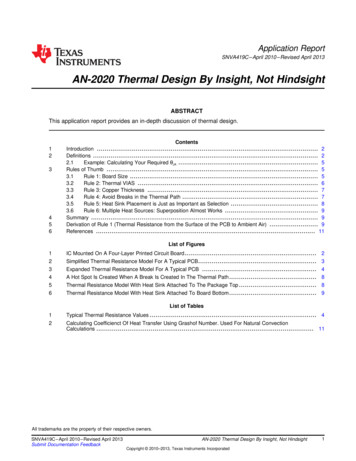
Introduction1www.ti.comIntroductionAll electronics contain semiconductor devices, capacitors and other components that are vulnerable tothermally accelerated failure mechanisms. Thermal design becomes vital to improving the reliability of anydesign. Unfortunately, thermal design can be very difficult because of the mathematical analysis of fluiddynamics for complex geometries. Although this remains true for the foreseeable future, this applicationreport covers the basics of thermal design for DC-DC converters using a simplified resistor model of heattransfer. Focus is on the thermal design for the semiconductor devices, but all of these techniques can beapplied to other components. The resistor model is very useful for quickly estimating your designrequirements, such as the PCB size and whether airflow is required. Finite element analysis software canthen be used to analyze the design in more detail. The listed reference material is home to additional dataand many useful thermal calculators, covering material that is beyond the scope of this document.Our discussion of thermal design will begin with the definition of parameters used in data sheets such asθJA and θJC, and end with some rules of thumb for the thermal design of a DC-DC converter, including theirderivation. An accompanying spreadsheet (see References) uses these derivations to quickly provide aballpark figure for the thermal performance of your design.2DefinitionsDescription of Thermal TermsParameters of interest : θJA, θJC, θCA, θJTSilicon Die (Junction)Exposed Pad (EP)Package BodyEP Landing Pattern2Top Copper Layer2Inner Ground Layer2 oz/ft (0.070 mm)1 oz/ft (0.035 mm)2Second Inner Layer1 oz/ft (0.035 mm)2Bottom Ground Layer2 oz/ft (0.070 mm)12 mil diameterThermal Vias1.6 mm r 10%Figure 1. IC Mounted On A Four-Layer Printed Circuit BoardThe most commonly specified parameter, in data sheets, for thermal performance is θJA. θJA is defined asthe thermal impedance from the Junction, of the integrated circuit under test, to the Ambient environment.If we describe it using a resistor model, it is the parallel combination of all the paths that heat can take tomove from the IC junction to the ambient air. The equation for this thermal resistance is:TJA TJUNCTION - TAMBIENTPower Dissipation(1)In our resistor model the heat transfer, measured in watts, takes the place of charge transfer measured inamps, and the temperature potential between the junction and ambient temperatures replaces the voltagepotential. The heat that needs to be transferred away from the junction is the power dissipated by the IC.2AN-2020 Thermal Design By Insight, Not HindsightCopyright 2010–2013, Texas Instruments IncorporatedSNVA419C – April 2010 – Revised April 2013Submit Documentation Feedback
Definitionswww.ti.comAmbient Air Temperature(TA)Junction Temperature(TJ)TTCase Top Temperature(TT)JTTAJCCATATJTCExposed Pad/Case Temperature(TC)JATJTAFigure 2. Simplified Thermal Resistance Model For A Typical PCBThere are two primary heat paths for a DC-DC converter represented above by their associated thermalresistances. The first path travels from the junction of the IC to the plastic molding at the top of the case(θJT) and then to the ambient air by convection/radiation (θTA). The second path is from the junction of theIC to an exposed pad (θJC). The exposed pad is then connected to the PCB, where the heat travels to thesurface of the PCB and to the ambient air by convection/radiation (θCA).There is one point of confusion that is common in defining θJC.For DC-DC converters without an exposed pad, θJC is defined as the thermal impedance from the junctionto the top of the case. This is in direct conflict with our previous definition of θJC, being the thermalimpedance from the junction to the exposed pad. This confusion comes about because of the largenumber of packages that DC-DC converters have been shoved into over the years. As newer packageswith exposed pads were released into the market it was decided that θJC should represent the lowestthermal impedance path from the junction of the IC to the outside world.Now that we have cleared up the terminology, we can discuss the usefulness of various parameters.Use the value of θJA given in the data sheet to compare different packages, and use it along with the ICpower dissipation for a sanity check in your design. The high thermal resistance of the plastic packagingensures that most of the heat travels from the exposed copper pad to the PCB, which usually has a muchlower thermal resistance. A heat sink can be added to either the top of the package or directly beneath theexposed pad on the backside of the PCB. Again, because of the high thermal resistance of plastic, a heatsink will be more effective when connected to an exposed metal pad, either directly or, through thermalvias.Since most of the heat transfer is through the exposed pad to the PCB it becomes immediately apparentthat the value of θJA is highly PCB dependant. In other words, the most critical value to determine in anydesign is thermal resistance of the PCB (θCA). Well what, exactly, is θCA and how is it calculated? θCA is theequivalent resistance of a thermal resistive lattice that centers on the IC and ends at the surfaces of theboard. It is the final of your freshman year, Circuits 101 class, all over again. Figure 3 below shows thedetails.SNVA419C – April 2010 – Revised April 2013Submit Documentation FeedbackAN-2020 Thermal Design By Insight, Not HindsightCopyright 2010–2013, Texas Instruments Incorporated3
Definitionswww.ti.comAmbient Air Temperature(TA)Junction CuCuSASASAFigure 3. Expanded Thermal Resistance Model For A Typical PCBThere are new terms to add to our ever growing lexicon of θ's. θCu is the thermal resistance of our board'scopper to lateral heat transfer. θFR4 is the thermal resistance between the copper planes provided by thevertical resistance of FR-4 laminate. θVIA is the thermal resistance of the thermal vias placed directlyunderneath the exposed pad. θSA is the thermal resistance from the surface of the PCB to the ambient air.It is a combination of convective and radiative heat transfer. If we break the board into 1 cm squares, thetypical values for these resistances are listed below.Table 1. Typical Thermal Resistance ValuesNam ValueeDescriptionConditionsθCuLateral thermalresistance ofcopper plane.Length 1 cm, width 1 cm,1 ounce copper thickness 0.0035 cm, thermalconductivity of copper (λCu) 4 W / (cm C)θVIA71.4 C /W261 C / W Thermalresistance oftypical 12 milvia.Via length 0.165 cm (65mils), 0.5 ounce copperplating thickness 0.00175cm, drill hole radius 6 mil(0.01524 cm), thermalconductivity of copper (λCu) 4 W / (cm C)EquationTCu 1 x LengthèCuArea C cmx 1 cmW1 cm x .0035 cm0.25 (2)1 x LengthOCuTVIA Area C cmx 0.165 cmW2S x [(0.01524 cm) - (0.01524 cm-0.00175 cm)2]0.25 (3)θSAθFR441000 C /W13.9 C /WThermalresistance fromthe surface of a1 cm square ofthe PCB to theambient air dueto naturalconvection.1 cm square, a first orderapproximation of the heattransfer coefficient of PCBBoard to Air for naturalconvection is (h) 0.001 W /(cm2 C)Vertical thermalresistance ofFR-4 substrate.1 cm square, FR-4 thickness 0. 032 cm (12.6 mil),thermal conductivity of FR-4(λFR4) 0.0023 W / (cm C)2 C cm11000Wh TSA Surface Area 1 cm x 1 cmTFR4 1 x ThicknessèFR4AN-2020 Thermal Design By Insight, Not HindsightCopyright 2010–2013, Texas Instruments IncorporatedArea435 (4) C cm x 0.032 cmW1 cm x 1 cm(5)SNVA419C – April 2010 – Revised April 2013Submit Documentation Feedback
Rules of Thumbwww.ti.comThe amount of variability in PCB designs is significant. You can see that the thermal resistance dependson board size, airflow, PCB thickness and many other parameters. For this reason, a series of JEDECstandards (JESD51-1 to JESD51-11) were developed, which specify the PCB size and layout for testingθJA for different types of packages. DC-DC converters that are tested to these standards can be directlycompared to one another. Always check the data sheet to see what PCB parameters were used tomeasure θJA. Later on we will discuss some tips for designing your PCB, but the final design, and thus θJA,depends on the end user.2.1Example: Calculating Your Required θJACalculate the θJA required for a DC-DC converter with an output voltage, VOUT, of 2.5V and output current,IOUT, of 4 amperes. The converter efficiency, η, is 91.4%. The ambient temperature, TA, is 50 C. Thecapacitors you selected are rated up to 100 C, and because of their proximity to the DC-DC converter youdecide that the maximum junction temperature, TJ, you would like the converter to reach is 90 C.The power dissipated by the converter, PD, can be easily calculated.PD VOUT x IOUT x ( 1 -1)PD 2.5V x 4A x ((6)1 -1) 0.94W0.914(7)Assuming that all of the power is dissipated internally to the IC, (a fair assumption if using LDOs ormodules) we can now calculate the maximum value of θJA.TJA 790 C - 50 C7 42.5 C/W0.94W(8)Since a θJA of less than 42.5 C / Watt is required for your design, you won’t get there with a SOT-23 whichhas a θJA closer to 179 C / Watt. You would need to select a package like the 14 Pin eMSOP with a θJA ofaround 40 C / W. If you would like to increase the thermal margins for your design, pick a package like theTO-PMOD-7 or TO-263, which have θJA's of around 20 C / W. Remember θJA is board dependant and allof these numbers come from using a JEDEC standard test board measuring 3” x 4”. If your board variesfrom the JEDEC board, which it will, you will need to get a better estimate of thermal performance byusing θJC, and deriving θCA.A package with a low θJC will have very good heat transfer to the case, usually to an exposed pad. θJC is avery good indicator of a packages thermal performance. A low value for θJA implies a low value for θJC.The θJC for packages designed to dissipate large amounts of power can be less than 2 C / Watt. Typically,packages with no exposed pad have a θJC of greater than 100 C / Watt. That means that for every wattdissipated in the package the temperature difference between the junction of the IC and case will increase100 C. If the value of θJC is not included in the data sheet it can often be requested from the manufacturer.3Rules of ThumbPCB DESIGN to meet a given θCAParameters of interest: θCAA low value for θJC (less than 10 C / Watt) is a good start for a thermal design, but we still need to designa PCB or heat sink to transfer the heat from the case to the ambient air. This section will provide simpleguidelines so that we can avoid calculating the full resistor model. The derivations for these rule
The amount of variability in PCB designs is significant. You can see that the thermal resistance depends on board size, airflow, PCB thickness and many other parameters. For this reason, a series of JEDEC standards (JESD51-1to JESD51-11)were developed, which specify the PCB size and layout for testing θJA for different types of packages. DC-DCconverters that are tested to these standards can be directly