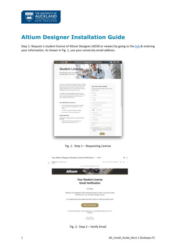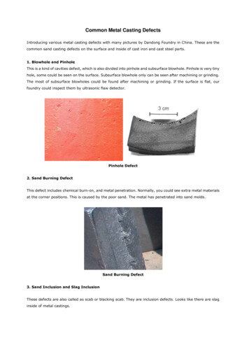
Transcription
Preventing PCB Defects
PREVENTING PCB DEFECTSPREVENTING PCB DEFECTSOne of the most important things you can do to make sure your PCB project goes off without a hitch is to be proactive from themoment of conception. As with many things in life, if you don't have a solid grasp of potential setbacks in your plans and how tocombat them, you may have a recipe for disaster. While you can stand to benefit from an honest discussion with peers about theirexperiences, trials, and errors, educating yourself on the technical aspects of the most common defects and how to prevent themwill serve you well for your entire PCB designing career. On top of boosting confidence in your process, knowing what to look out for(and how to prevent problems that could arise later on) will be a major asset in ensuring that your board will be the dependable,quality product you had in mind.Join us as we discuss topics related to preventing PCB defects, including:PCB Design for Manufacturing: Prevent Via Defects by Talking to Your ManufacturerHow to Prevent Hairline Short Circuits in Your PCB Circuit DesignRF Interference Prevention and RF PCB Design in the Internet of ThingsUsing Circuit Making Software for DFM: How to Prevent TombstoningMicrocontroller Failure Modes: Why They Happen and How to Prevent ThemImportant Considerations for Pads in PCB Design: Pad Cratering Preventionwww.altium.com
PREVENTING PCB DEFECTSPCB DESIGN FOR MANUFACTURING: PREVENT VIA DEFECTS BY TALKINGTO YOUR MANUFACTUREROne of my ex-girlfriends always used to say, “communication is key for our relationship.” While I may be good at communicating howto reduce EMI on boards, I’m not so good at expressing my emotions. I guess that’s why she’s an ex-girlfriend. Sometimes yourfeelings toward your manufacturer may resemble your feelings towards any ex-girlfriends. Especially when they tell you that yourboards have a 50% yield.At that point, you may feel like replying with some choice words. Talking is still the answer, just not that kind. Having a discussion withyour manufacturer on the front end will reduce manufacturing defects and fabrication costs.www.altium.com
PREVENTING PCB DEFECTSThose little holes can cause more problems than you think.REDUCE MANUFACTURING DEFECTSEveryone wants to date the perfect person, but that’s just not going to happen. Luckily, we can make up for our romanticshortcomings by designing excellent PCBs. Like flaws in that perfect person, defects in PCBs tend to show up over time. It’s better tojust avoid them altogether by going through your design with your manufacturer. There are lots of things to check through, but yourtop priorities should be via-in-pads, filled or capped vias, drilling methods, and surface mounted technology (SMT) pads.Via-In-Pads (VIPs) - You should know what VIPs are, they’re literally vias placed inside pads. VIPs will help you with ball gridarray (BGA) breakout but can cause issues as well. If not properly addressed, VIPs can wick solder paste away fromcomponents and cause bad connections or tombstoning. You can avoid those problems by plating over any VIPs. Plated VIPswill need to be either filled or plugged, which is where your manufacturer comes in. Talk with them about their methods forfilling or plugging, and then plating, any VIPs on your board.Capped or Filled Vias - In a related note, you should also talk to your manufacturer about any general vias that need to becapped or filled. Some people think they can slightly offset a via from a pad and it will be fine. Those people are wrong. Even ifyou’re using something like a dog bone breakout, solder paste can still wick down into vias. So guess what, you have tocap/tent/cover, plug, or fill them. Again, different methods have different pros and cons, many of which will depend on yourmanufacturer’s capabilities.Drilling Methods - Let’s keep the via ball rolling. You need to go over how your vias will be drilled with your manufacturer.www.altium.com
PREVENTING PCB DEFECTSThrough vias are no problem, but drilling can cause some problems when it comes to blind and buried vias. Vias can eitherbe drilled mechanically or with lasers. Lasers don’t usually have many fabrication problems, because they’re awesome.Mechanical drilling, however, is not awesome. Some manufacturers may recommend “peck drilling” your blind or buried vias.Peck drilling is where the drill moves in and out of a blind hole in order to remove drilled material. The problem is, thismethod can cause material or air to become trapped inside the hole during plating. Air during plating means the via won’t befully plated, causing connection problems.Pads - Not only will you need to worry about vias next to pads, you’ll need to think about the pads themselves. If pads are tooclose together, or if you accidentally forget some solder mask, solder paste will bridge pads. This is usually more a product offorgetfulness rather than bad design. You might miss this mistake, but your manufacturer will be looking for it.Defects can make you go crazy, like this poor engineer trying to jump a PCB.REDUCE COSTChanging your mind after getting married will cost you an arm and a leg. Likewise, you’ll pay a high price for changing designspartway through manufacturing. Checking your designs with your manufacturer can save you a pretty penny.You should also run your design by your manufacturer to see if it will require expensive fabrication processes. Sometimes yourmanufacturer can suggest a different design that will be less expensive to fabricate, or a different process that can lower cost.Remember how I was blathering on earlier about how blind vias can be laser drilled or peck drilled. Well, why would you ever peckwww.altium.com
PREVENTING PCB DEFECTSdrill when lasers are cooler and have less risk for defects? Peck drilling is cheap, that’s why. Some manufacturers are actually able topeck drill without causing defects. They could be that mythical perfect partner you’ve been looking for. If your manufacturer can dothings like peck drilling correctly, they can save you a lot of money. Sweet talk them and see what their capabilities are.Be sure to check individual parts as well, for example ct25664aa800.You may love your partner, but we both know that PCB design is your mistress. Clearly communicating with your manufacturer willhelp you address the flaws in your relationship with PCBs. Enlist their aid in avoiding defects in your vias and pads, and in savingmoney.As I said earlier, talking to your manufacturer will help you, but it’s better to design a great board on your own. In order to do thatyou’ll need some pretty advanced PCB design software. Altium Designer is the program for you. Altium Designer has already helpeddesigners design for manufacturing. Think I’m just blowing hot air? Hear from Sierra Circuits about how Altium Designer has madetheir manufacturing job a breeze.Want to learn more about design for manufacturing? Talk to an expert at Altium.www.altium.com
PREVENTING PCB DEFECTSHOW TO PREVENT HAIRLINE SHORT CIRCUITS IN YOUR PCB CIRCUITDESIGNWhat’s worse than finding a strand of hair in your pasta when you’re out on a dinner date? Finding it after it has ended up in yourmouth. There are two ways to avoid awkward scenarios like this. For one, you can keep a close eye on your food and make sure it ishair free before it enters your mouth. The second is to ensure that there is no chance of a hair ending up in your food; in this case,you might need to go to a new restaurant. In PCB design, dropping a couple strands of hair won’t cause much damage, but having asingle hairline short circuit on a PCB can be rage inducing in QC. The time taken to identify a single hairline short circuit and the costof fixing it can sometimes cost more than the assembled PCB. Much like dining at restaurants that leave a hair in your food, it’s bestto avoid adding hairline short circuits to your design. That being said, we’re all capable of making mistakes. You might not be able tocompletely avoid them, but you can employ these best practices to minimize their likelihood.WHAT IS A HAIRLINE SHORT CIRCUIT AND HOW DO THEY HAPPEN?A short circuit occurs from an unintended connection between two unrelated signals. For example, when the positive voltageconnection is connected to the ground signal, it is considered a short circuit. Short circuits are visible to the naked eye if the signalsare connected by thick copper. This can happen if your PCBs are being produced manually rather than machine manufactured.www.altium.com
PREVENTING PCB DEFECTSHairline short circuits are a concern when PCBs are machine manufactured. This is because copper, that is as thin as a strand of hair,can end up connecting two different signals. This sort of short circuit can go undetected by the naked eye until the assembled PCBsare put through a series of QC tests. Unfortunately, if a short circuit is detected this late in the production cycle then it is guaranteedto cause unnecessary losses in time and raw material costs.To understand how short circuits happens, you need to understand the general process of PCB manufacturing. PCBs are typicallymade of copper laminated on a non-conductive substrate. A common method to transfer the circuitry onto the PCB is throughphoto engraving, where a silk screen laminate containing the image of the circuit is placed on top of PCB made with photoresistcoating.The PCB is then exposed to ultraviolet (UV) light source and any areas that are not covered by the silkscreen will be etched away byan ammonia based solution. These processes are mostly automated, and an imperfection in the procedure could leave a thin line ofcopper connecting pads or tracks of different signals. Without thorough post-manufacturing testing, this can cause unnecessaryproblems later in the production stage.In most cases, locating a hairline short is nearly impossible until it’s too late.HAIRLINE SHORT CIRCUITS CAN BE REDUCED WITH PROPER ELECTRICAL TESTINGAs a self-taught PCB designer, one of my greatest and most painful lessons was not putting my PCBs through post-manufacturingelectrical testing. It’s not safe to assume that your PCB manufacturer will perform all the necessary electrical checks postmanufacturing. Make sure that your PCBs pass an electrical test like the Flying Probe Test before they are sent for assembly. TheFlying Probe Test moves high precision probes at high speeds over your component pads and vias to uncover any manufacturingfaults and design errors.Bear in mind that electrical testing does not guarantee a 100% error free PCB since hairline short circuits can occasionally escapewww.altium.com
PREVENTING PCB DEFECTStesting. However, it greatly reduces the chances of a faulty PCB being sent for assembly. To further reduce your risks, you shouldensure that your PCB manufacturer has a reimbursement policy for each faulty PCB that passes the electrical test. In such cases,reputable manufacturers will replace the faulty PCB and reimburse the cost of the assembled components.Always have your PCB tested before they are assembled.WHAT CAN DESIGNERS DO TO REDUCE THE POSSIBILITY OF HAIRLINE SHORT CIRCUITS?While hairline short circuits are often a fault of PCB manufacturing, electronics designers can do their part to reduce their probability.Depending on how tight your design constraints are with respect to form factor or your budget, it is a good practice to opt for alarger clearance between copper connections and pads.While there are no studies linking hairline short circuits with the clearance distance between copper traces, I have learned fromexperience that hairline short circuits are more likely to occur in compact and complicated PCB designs. To minimize this issue, I’veavoided pushing the manufacturing capability of my suppliers to the limit, and I try to maximize the clearance tolerances in mydesigns when it is possible.For instance, if a supplier specifies that it’s capable of handling 5 mil trace width and clearance, I’ll set my design’s clearance limit to 6mil. When I’m dealing with new suppliers, this is a practice I always employ. As engineers, it is always prudent to test the limits ofmanufacturers on a smaller scale, instead of risking the whole batch of production.High-quality PCB design software allows you to set customized clearance rules so that you can check your designs before finalizingthe files for production. CircuitStudio’s Clearance Matrix is a design tool that’s helped me keep my copper connections apart.Have a question? Contact an expert at Altium to find out more about clearance rules.www.altium.com
PREVENTING PCB DEFECTSRF INTERFERENCE PREVENTION AND RF PCB DESIGN IN THE INTERNETOF THINGSHave you ever been to a party where there was so much noise you could barely hear yourself think? I’m a dedicated introvert, butsometimes my friends lure me out to such gatherings with promises that it will be “very relaxed.” They never are, and I don’t seem tolearn. It’s times like those that I wish it was socially acceptable to wear noise-canceling headphones to such events. In the world ofelectronics, the burgeoning Internet of Things (IoT) is starting to make the RF spectrum look like a rowdy party. It’s likely that yourdevice is going to have to deal with interference coming from other “things.” Fortunately, it’s acceptable and even recommended, toequip your board with the PCB equivalents of noise-canceling earphones.CROWDED SPECTRUMSI once threw a party in my house in college. Unfortunately, we lived in a duplex and the neighbors who shared our wall called thecops at 9 PM. If you want to be noisy out by yourself, no one really minds, but many of the most useful spectrums are getting packedout. Even if nearby bands are vacant today, they could be occupied in the near future.The RF spectrum as a whole is starting to get a bit crowded. Even more so specific bands are chock full of devices. For example,nearly everything we use in our homes runs on 2.4 GHz. My WiFi used to go out when I turned on the microwave until I added somewww.altium.com
PREVENTING PCB DEFECTSextra shielding. That’s the kind of interference your next IoT gizmo is going to face in the home. It’s not just going to be from themicrowave, though, it could come from anyone else’s “smart” widget as well.Even if you’re working in a relatively quiet spectrum, it could soon become crowded. That’s happening to the mm-wave spectrumright now, as it’s been opened up for 5G and other high speed communication protocols. Just because don’t have to deal with loudneighbors at the moment, doesn’t mean they won’t move in soon.The IoT is becoming as loud as this child’s birthday party. Give your device earplugs.DESIGNING FOR IMMUNITYYou may be feeling as overwhelmed as I do when at a party, but have no fear, there are ways to protect your PCB from unwantedinterference.Shielding - This is probably the option you thought of first as well. Shielding your board or its sensitive components greatlyreduce the threat of troublesome EMI. While this is the most straightforward approach, it could interfere with yourtransmissions and will add cost.Proper Grounding - Grounding your PCB well is essential to managing onboard and incoming EMI. If your board is groundedcorrectly it can reduce the effects of EMI on your board. A complete ground plane can also act as a shield for your circuits. Ifyou want to shield certain components but don’t have the budget for an extra one, use the ground plane instead.Careful Routing - Long high speed routes are notorious for radiating EMI, but they can also receive it as well. Lengthy tracescan act as both transmitters and receivers of EMI. Even if your dedicated antenna can reject interference, you may havewww.altium.com
PREVENTING PCB DEFECTSseveral unintentional ones that are at risk. Keep your runs short to avoid this problem.Your primary antenna might not be the only thing receiving incoming signals.SILENCE IS GOLDENSome people don’t know how loud they speak and never realize that they’re the problem. I don’t want to be a buzzkill, but make sureyou’re not that person. Your device may be the noisy one, make sure you test it to ensure that’s not the case.Let’s face it, no one likes dealing with radiated or conducted emissions testing. It’s a huge hassle and can also be quite expensive. Ifyou’re up to the task, though, you can buy or rent your own equipment and take matters into your own hands. Radiation testingrequires a good bit of equipment, but it’s not overwhelming. Conducted emissions tests can be simpler to conduct and require lessgear. Even if you can’t do everything yourself, a little pre-compliance can go a long way and save you money in repeat visits to acertification lab.The IoT and the spectrums it operates on are getting more and more crowded. All kinds of devices are radiating EMI, and if you’renot prepared it could affect your device’s operation. Careful PCB level design can help eliminate or at least mitigate the effects ofincoming interference. You also need to be certain that your gadget isn’t the one causing problems and bothering other people’sgizmos.Designing a board that is immune to EMI is a difficult task. I can’t do it all for you, but good PCB design software like Altium'sCircuitStudio can help. It has a range of great tools and features that can help you design a great board for the IoT.Have more questions about EMI? Call an expert at Altium.www.altium.com
PREVENTING PCB DEFECTSUSING CIRCUIT MAKING SOFTWARE FOR DFM: HOW TO PREVENTTOMBSTONINGHalloween, it’s that time of year again. Soon the streets will be filled with children dressed up in their scariest costumes ringing yourdoorbell and yelling “Trick or treat!” Already there are spooky decorations everywhere, and graveyard scenes seem to be one of themost popular themes.There aren’t many things in life more frightening than the idea of weird and unnatural occurrences in a graveyard. Did you knowthough that a weird graveyard-like thing can happen right on the printed circuit board that you’ve just designed? I’m talking abouttombstoning. During the reflow solder process, your smaller passive chip components may lift up on one side and stand straight uplike a tombstone. If you haven’t heard of this before, take a look at this short video. Doesn’t that just scare the socks off of you? CallScooby and the gang, we’ve got a mystery to solve!As you can see from the video, tombstoning is a very real manufacturing problem that can be prevented with tighter designstandards and more accurate manufacturing processes. Let’s take a look at some of the causes of tombstoning and how you canhelp to prevent it.www.altium.com
PREVENTING PCB DEFECTSMANUFACTURING ISSUES THAT CAN CAUSE TOMBSTONINGThe root cause of tombstoning, which is also known as the “Manhattan effect” or the “drawbridge effect”, can be traced to unevenwetting forces on the component during solder reflow. If the solder on one end of the component melts before the other end, it willcause an imbalance in the soldering process. This imbalance between the two terminal ends of the component can pull thecomponent towards the wet or melted side, and cause the tombstoning effect.There are many factors that can contribute to this solder imbalance. One of those is an incorrectly placed component that is notaligned on its pads. You can see how the misaligned component pulls towards the pad that it has the most contact with.In addition to incorrectly placed components, there are other factors that can contribute to the tombstoning effect:Solder paste printing that is uneven.Uneven temperatures in the reflow oven.Different thermal conductivity of PCB materials.These are problems that can only be resolved by improving the accuracy of the manufacturing processes. If your manufacturer isunable to resolve these kinds of problems, it may be time to look elsewhere. There are other contributing factors that you canaddress on the design side though that will help to mitigate the tombstoning problem.Passive chip components soldered on a PCB.www.altium.com
PREVENTING PCB DEFECTSHOW TO PREVENT TOMBSTONING USING CIRCUIT MAKING SOFTWAREOne area of design where you can really help to reduce the chance of tombstoning when working with circuit making software is inthe component pad patterns. If the pads that you are using are not the correct size for the component, or if they are spaced too farapart, it can affect the thermal mass of the solder joints. If a solder joint has less mass than its solder will reflow sooner. The wetsolder will then exert a pulling force on the component that may overwhelm the other end and cause the component to tombstone.You can avoid these problems by following the manufacturer’s DFM rules when creating your pad shapes.The orientation of components on the board can also contribute to solder reflow problems. A component that is oriented on theboard so that it travels parallel through the oven’s conveyor will have one terminal end heated before the other. This can also lead totombstoning. Passive chip components should be oriented so that both ends are heated at the same time whenever possible.Another area where you can help reduce the tombstoning problem is in making sure that the two pads of the component are thesame size. Different sized pads on the same component will have different thermal masses, which will cause one pad to reflowbefore the other one resulting in tombstoning. This shouldn’t be a problem though since it is typical to use the same pad shape forboth pins of the component.Inspecting the quality of soldered components on a PCB.MANAGING THE CONFLICT BETWEEN DESIGN AND MANUFACTURINGAs we discussed earlier, the pad shapes for the two pins of a passive component should be the same size. However, this bestpractice for manufacturing can conflict with the routing requirements. Electrical considerations often dictate that one side of thecomponent should have a very wide trace to connect it to power or ground and that connection is usually made to a plane directlythrough a via. Meanwhile, the other side of the component is usually connected through a thin trace.www.altium.com
PREVENTING PCB DEFECTSAlthough the pad shapes are the same size, the different sized routing may cause the thermal mass of the pads to be different fromeach other. The wider traces, via, and ground plane will act as a heat sink for the pad that they are connected to. This will cause thepad to take more time to heat up than the pad that has the thinner traces on it. The result of all of this is a reflow timing differencebetween the two pads that can cause the component to tombstone.This situation is the classic dilemma of the circuit designer; trying to satisfy the needs of both electrical engineering andmanufacturing. In this case there isn’t a “right way” or a “wrong way” to resolve the problem. The best thing that you can do is to getboth electrical engineering and manufacturing to agree on a strategy that will satisfy all needs of the design.Plastic decorations of graveyard tombstones shouldn’t fill us with fear, but we should have a lot of respect for tombstoning partsduring manufacturing. Now that you have a better understanding of what the problem is, you will be better prepared for it. Withgood design practices and open communication with your manufacturer, you will be able to bury this problem for good.Circuit making software, like Altium Designer, has different placement utilities and other functionality built into it to work togetherwith your DFM rules. Would you like to find out more about the different design options that Altium offers its users? Talk to anexpert at Altium.www.altium.com
PREVENTING PCB DEFECTSMICROCONTROLLER FAILURE MODES: WHY THEY HAPPEN AND HOW TOPREVENT THEMI owe much of my design success to my college. Not because of the lab experiments where we learned what might accidentally blowup a capacitor, but because we learned that Murphy’s Law can strike when you least expect it to. Since I spent a lot of time playingWarcraft and struggling to finish up endless assignments, I relied on my computer to function at all times.Back then, computers were pretty limited and it wasn’t uncommon to see the infamous Windows “Blue Screen Of Death” popup oncein a while. While it’s frustrating to get interrupted from a game of Warcraft; losing hours of unsaved assignments to a systemcomputer crash would send me into a massive panic attack. As a designer, you might have experienced a similar panic when yourmicrocontroller fails in the field.HOW MICROCONTROLLER FAILURE MODES EFFECTS A SYSTEMIn an embedded system, microcontroller (MCU) failures could have worse repercussions than missing your assignment’s deadline.MCUs are often the heart of applications like payment machines, medical devices, and security systems. These systems demand highstability and often have low tolerances for system failures.An MCU that has failed can cause a complete standstill in operations. This can inconvenience users or pose safety risks in criticalwww.altium.com
PREVENTING PCB DEFECTSapplications. For the clients, unreliable systems affect the operational capacity and potentially cause losses in revenue. For designers,having hundreds of their products constantly failing in the field is a huge blow to our pride, and can affect our reputation.Pointing fingers doesn’t help a microcontroller that’s failed.WHY A MICROCONTROLLER FAILS AND WHO SHOULD BE RESPONSIBLEA reliable embedded system requires a combined effort from the hardware designer and the firmware programmer. Some designfaults can go undetected during the development phase and only rear their ugly heads once deployed. When this is the case, whoshould bear the larger portion of the responsibilities?Before we start pointing fingers, let’s have a look at the common reasons why microcontrollers fail.1. Memory Stack Overflow- A microcontroller’s memory stack is a designated area of its internal RAM that is used meant fortemporary usage. The size of a memory stack is limited and varies with different MCUs. When the firmware programmer allocates avariable greater than the stack size, a stack overflow may occur during the runtime and cause the firmware to fail.2. Illegal Pointers- In MCU firmware programming, a pointer is commonly used to indicate the address of a variable or programfunctions. Declaring and using pointers requires the firmware programmer to adhere to the strict syntax defined by theprogramming language, often in C. Introducing an illegal pointer by mistake can cause the MCU to attempt to process variables orfunctions in addresses that are outside its valid range. This could crash the MCU.3. Unstable Voltage Source- Often an overlooked factor, an MCU needs stable power network to run reliably. MCU could fail when itspower source is constantly disrupted by external interference. A dip in the operating voltage could cause an MCU to behaveerratically or freeze completely.4. Electrical Interference- Failing to handle electrical interference, especially those induced from relays and motors could crash yourwww.altium.com
PREVENTING PCB DEFECTSMCU. During one of my earlier projects driving a simple DC motor, my MCU failed each time it tried to drive the motor in reverse.This problem was solved by increasing its electrical isolation using an operational amplifier.5. Poor Assembly Processes- Occasionally, a microcontroller fail can have nothing to do with both the hardware or the firmwareengineer. Low-quality solder joints on the MCU pins can result in unpredictable MCU behavior. If only a handful of your embeddedsystems are failing, you might start to investigate the process quality of your manufacturer.Your design is as good as your PCB assembler.Instead of playing the blame game, both hardware and firmware engineers must play their part in designing a reliable embeddedsystem. Practicing good programming ethics and planning memory allocation beforehand are best practices to follow. Forprogrammers, keeping things simple can be a wise choice for minimizing buggy codes.Hardware designers need to consider the environment that the hardware will be used in and prepare for all possibilities. This meansadhering to all the best basic design practices and fully utilizing your PCB software’s tools to test the design. Altium’s CircuitStudio,which is built with Altium Designer technology, gives you the tools to design professional PCBs.Contact an expert at Altium to understand why your microcontroller is failing.www.altium.com
PREVENTING PCB DEFECTSIMPORTANT CONSIDERATIONS FOR PADS IN PCB DESIGN: PADCRATERING PREVENTIONEvery year after Halloween, my school used to have a pumpkin launch, probably so they could get the pumpkins on sale. Mostly,mechanical engineering students participated, but anyone was allowed to enter and see if they could launch their pumpkin thefarthest. Sections of campus were blocked off and your path to class was rerouted if you went at all. Most of the engineers got (ortook) the morning off for cheering and jeering.Results were haphazard. We had occasional glorious pumpkin flights, but most pumpkins really didn’t make it very far. However, oneyear, a pumpkin somehow got launched straight up, and we all raced around shrieking in excitement, unsure of where to seek cover.The total lateral distance covered was about a meter, so the spectators were in no danger, but the perfectly coiffed lawn took somedamage. New launch regulations were hotly debated with the administration for the rest of the year since apparently late fall is adifficult season for repairing pumpkin craters in the turf.I think craters in all forms should be accompanied by that level of frantic energy. On a PCB, pad cratering sounds like it should becaused by tiny flaming meteorites, or something comparably dramatic. In reality, the “craters” result from a pad separati
www.altium.com PREVENTING PCB DEFECTS One of the most important things you can do to make sure your PCB project goes off without a hitch is to be proactive from the moment of conception. As with many things in life, if you don't have a solid grasp of potential setbacks in your plans an