Transcription
International Journal of Engineering Trends and Technology (IJETT) – Volume 48 Number 4 June 2017Transformer Inrush Current Mitigation forSeries Voltage Sag CompensatorAnil Kumar Pathak1Dr. A. K. Jhala2 Pramod Kumar Rathore31M. Tech Department of Electrical & Electronics Engineering RKDF-CE, Bhopal (MP) IndiaAssociate Professor Department of Electrical & Electronics Engineering RKDF-CE, Bhopal (MP) India3Assistant Professor Department of Electrical & Electronics Engineering RKDF-CE, Bhopal (MP) India2Abstract- Manufacturing industries are located inindustrial park. Survey results suggest that 90% ofinterruption at industrial facilities is related voltagesag. An inrush mitigation technique is proposed andimplemented in a synchronous reference frame sagcompensator controller.Thevoltagesagcompensator is based on three phase voltage sourceinverter and a coupling transformer for serialconnection. In various companies voltage sag mayaffect many manufactures and may reduce theefficiency of the system which results sufficientlosses in the power system. It is the most costeffective solution against voltage sags. When voltagesag happen, the transformers, which are ofteninstalled in front of critical loads for electricalisolation, are exposed to the disfigured voltages anda DC offset will occur in its flux linkage. Atransformer inrush may occur at the start of sagcompensator. This over current may damage theinrush protection of the series connected inverterand the transformer output voltage is greatlyreduced due the magnetic saturation. When thecompensator restores the load voltage, the fluxlinkage will be driven to the level of magneticsaturation and severe inrush current occurs. Thecompensator is likely to be interrupted because of itsown over current protection. This paper proposes aninrush current mitigation technique together with astate-feedback controller for the Voltage sagcompensator.Keywords- SVPWM, Inrush current, Voltage sagcompensator.I. INTRODUCTIONTo strengthen the power network stability bymitigating the power quality issues. The study showshow much work is done in the field of power qualityand what can be done to increase reliability andstability.The main objective of the dissertation can begrouped as follows-ISSN: 2231-5381 Balancing the active and reactive power in powersystem. To maintain voltage profile across power systemby reducing the inrush current in the distributionsystem. Various methods and their effect on distributionsystem. To study the harmonic distortion due to variousmethods used for inrush current mitigation.Problem Formulation: The Electrical Power Systemis a very large network in which number of powerquality issues may occurs such as voltage sag/swell,harmonics, interruptions, transients, voltagefluctuation, noise, notching. In a power systemdifferent types of loads are connected across loadside as well as source side of system. In survey it isfound that most of the interruption at industrialfacilities is voltage sag related. Voltage sag is a mostinfamous problem as it goes on affecting a largenetwork.As the power network, consist of large numbers oftransformers which are affected by inrush currentdrawn due to sudden loading. Hence inrush currentacross the transformer also create the voltage sagwhich is not addressed in any voltage sagcompensator. A system to mitigate the inrush currentis required to minimize the voltage sag in thenetwork. Hence proposed mitigation techniquereduces the inrush current in distribution powersystem.Work Methodology:The dissertation will focus on the concept ofmitigation technique of power quality issues (inrushcurrent mitigation) and how they can be used tomaintain the power distribution system reliabilityand stability. Simulation of inrush mitigation technique withseries voltage sag compensator in MATLAB andits behavior when disturbances are applied on thesystem under critical load condition and also withdifferent control technique PWM & SVPWM. Study of different control techniques used formitigation.http://www.ijettjournal.orgPage 187
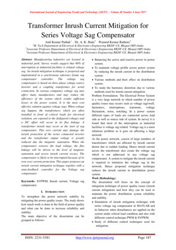
International Journal of Engineering Trends and Technology (IJETT) – Volume 48 Number 4 June 2017 Simulation and implementation of mitigationtechnique with series voltage sag compensator inabove simulation of test system. Analysis, performance and calculation of inrushmitigation technique with series voltage sagcompensator for different as well as online andoffline load conditions.II. PROPOSED METHODOLOGYWhen the grid is normal, the compensator isbypassed by the thyristors for high operatingefficiency. When voltage sags occur, the voltage sagcompensator injects the required compensationvoltage through the coupling transformer to protectsensitive loads from being interrupted by sags.However, certain detection time (typically within4ms) is required by the sag compensator controllerto identify the sag event. And the load transformer isexposed to the. Deformed voltage from the sagoccurrence to the moment when the compensatorrestores the load voltage. Also its short duration, thedeformed voltage causes magnetic flux linkagedeviation inside the load transformer, and magneticsaturation may easily occur when the compensatorrestores the load voltage, thus results in inrushcurrent. The inrush current could trigger the overcurrent protection of the compensator and lead tocompensation failure thus this paper proposes inrushmitigation technique by correcting the flux linkageoffsets of the load transformer. This technique canbe seamlessly integrated with the state feedbackcontroller of the compensator.compared with reference phase voltages. A carrierindex, I, is defined to designate the carrier regions inwhich the reference phase voltages lie during thesampling interval under consideration. When n isodd. The carrier index I for the top carrier is 1, and itincreases in steps of 1 towards the bottom carriers.The carrier index I for the lowest carrier is equal to(n-1). During a sampling interval, the carrier indices,, and (which can be from 1 to (n-1), for A, Band C phases, respectively, are determineddepending on the carrier region in which therespective phase voltage lies. The determination ofthe time durations,,, and.When n is odd, can be generalized as(1)(2)(3)When n is even, the triangular carrier & referencephase voltage, are as shown in this case, thereference phase voltage are centred on the middletriangular carrier. The determination of,, andcan be generalized as(4)(5)(6)Space vector is employed as it is an advancedtopology from the conventional PWM techniques.Space vector PWM technique is an advancement ofsinusoidal PWM as the pulses produced by digitalswitching of the fundamentalwaveform.Considering six switch operation we divide the VSIinto two parts as upper part and lower part. Theupper part contain the switches S1 S3 & S5 leavingthe lower part of the VSI with S2 S4 & S6.TABLE 1. SWITCHING STATESFig. 1. Simplified One Line Diagram of the Off-Line SeriesVoltage Sag Compensator Generalization of the Proposed SVPWMScheme for An n' Level PWM Inverter:The SVPWM, proposed for a three-level inverter,can be easily extended to any n-level PWMgeneration. In the SPWM scheme for an n levelinverter, the reference signals are compared with(n-1)level shifted carriers The triangular carriers and thereference signals, for an n-level PWM scheme, for nis odd, for n is even. The (n-1) triangular carriers areISSN: 2231-5381Switch1st Mode2nd Mode3rd mode4th Mode5th Mode6th Mode7th Mode8th 1S301010101Page 188
International Journal of Engineering Trends and Technology (IJETT) – Volume 48 Number 4 June 2017The signal generation of space vector is compared tothe triangular waveform to generate three PWMpulses to which NOT gates are given to get the otherthree pulses. The control signal of space vectorPWM is given blow fig. 2Fig. 3. Per phase equivalent circuit of the voltage sagcompensator series(7) (8)TWhereTFig. 2. Control signals of Space vector PWMTIII. SYSTEM CONFIGURATION OF THEPROPOSED COMPENSATORThe series compensator is consisted by a three phasevoltage source inverter. The leakage inductor ofcoupling transformerand capacitorisrecognized as the low-pass filter to suppress PWMripples of inverter output voltage . Fig. 3 showsthe equivalent circuit of series voltage sagcompensator and its dynamic equation can beexpressed as, is the inverter output voltage,is the filter inductor current,is the compensation voltage, andT (9) (10)IV. SIMULATION AND RESULTS ANALYSIS Simulation with proposed mitigation technique(PWM):Fig. 4. Simulation model with mitigation technique (PWM) a)Output waveforms:Source voltageISSN: 2231-5381http://www.ijettjournal.orgPage 189
International Journal of Engineering Trends and Technology (IJETT) – Volume 48 Number 4 June 2017Fig. 7. Load Current waveformFig. 5. Source voltage WaveformD)Magnetic Flux of Load Transformerb) Load VoltageFig. 8. Magnetic Flux WaveformFig. 6. Load Voltage WaveformFig. 5 shows the input source voltage waveformand Fig. 6 shows load voltage waveform which isget stabilized to normal value due to inrushmitigation technique.C) Output load current Offline mitigation technique (SVPWM) :Fig. 9 shows the simulation model with inrushcurrent with online mitigation technique with seriesvoltage sag compensator in which space vector pulsewidth modulation (SVPWM) technique is used.In offline mitigation technique at 0.3 sec loadconnected without compensator at 1 seccompensation on, from 1.5 to 2 sec load isdisconnected, at 2 sec and 2.3 sec load 2 and 3connected with compensation.Fig. 9. Simulation model With Migration Technique (SVPWM)ISSN: 2231-5381http://www.ijettjournal.orgPage 190
International Journal of Engineering Trends and Technology (IJETT) – Volume 48 Number 4 June 2017A)Source voltagesystem in which at 1 sec due to mitigation techniqueflux linkage in load transformer is reduced.Fig. 13. Magnetic Flux WaveformFig. 10. Source voltage waveformHarmonics Analysis:B)Load voltageTABLE 2 TOTAL HARMONIC DISTORTION ANALYSISRESULTSr. No.12Fig. 11. Load Voltage WaveformFig. 10 shows the input source voltage waveformFig. 11 shows the output load voltage waveformwhich is get stabilized to normal value due to inrushmitigation. At 0.3 sec load connected withoutcompensation so load voltage waveform get disturbup to 1 sec where compensation on. After 1 secwaveform get stabilized.c)Output load currentFig. 12. Load Current waveformd) Magnetic Flux of Load TransformerAs shown in magnetic flux waveform in Fig. 13 theflux linkage in load transformer increases due tovoltage sag occurs by connection of critical load inISSN: 2231-5381Mitigation TechniquesPWM TechniquesSVPWM TechniquesTHD value5.06%3.54%V. CONCLUSIONAs the distribution system is connected with numberof critical load, electronics load which are verysensitive load as change in supply occurs they getdamage to avoid this need of mitigation of inrushcurrent is required.In this dissertation work, a new technique usedfor mitigation of transformer inrush current has beenpresented and simulated. A relative comparativestudy was done with and without mitigationtechniques. The proposed technique based on thethyristor control pulse width modulation (PWM) andspace vector pulse width modulation (SVPWM)control. SVPWM technique offers flexible control ofoutput voltage as well as harmonic reduction. Withthe above topology in a simple test grid system withnon-linear load the voltage profile of the system ismaintained even in the different load condition also. We have studied, designed and simulate inrushmitigation technique of load transformer forseries voltage sag compensator with differentcompensator technique and found that theSVPWM technique is better over PWMtechnique and system goes on improving theperformance. We also have tested results for two different loadcondition and we can conclude that thistechnique can be used for different loadconditions. We also have done graphical comparison of pulsewidth modulation (PWM) and space vector pulsewidth modulation (SVPWM) on the basis of totalharmonic distortion (THD) and it is found thathttp://www.ijettjournal.orgPage 191
International Journal of Engineering Trends and Technology (IJETT) – Volume 48 Number 4 June 2017SVPWM control technique offers less harmonicdistortion as compare to PWM control technique.ReferencesREFERENCES[1]D. Sabin, An assessment of distribution system powerquality, Elect. Power Res. Inst., Palo Alto, CA, EPRI FinalRep. TR-106249-V2, vol. 2, Statistical Summary Report,May 1996.[2] C. J. Huang, S. J. Huang, F. S. Pai, Design of dynamicvoltage restorer with disturbance-filtering enhancement,IEEE Transactions on Power Electronics, vol.18, pp.12021210, Sept. 2003.[3] P. K. Lim, D.S. Dorr, Understanding and resolving voltagesag related problems for sensitive industrial customers,IEEE Power Engineering Society Winter Meeting, vol.4,pp.2886-2890, 2000.[4] P. T. Cheng, C. L. Ni, J. M. Chen, Design of a statefeedback controller for series voltage sag compensators,Power Conversion Conference, pp. 398-403, April 2007.[5] Po-Tai Cheng An Inrush Mitigation Technique Of loadTransformers For The Series Voltage Sag Compensator9784244-1668-4/08/ 25.00 2008 IEEE.[6] Yogesh K Chauhan Bhavnesh Kumar and Sajid Ali.GBUStudy and Performance of DVR for Voltage QualityEnhancement 987-1-4673-6150-7/13IEEE2013.[7] Ajinkya M. Bhaware, 2M.F.A.R Satarkar Series TransformerInrush Mitigation Technique during Change in Load forDistribution System Proceedings of 32nd IRF InternationalConference, 12th July 2015, Pune, India, ISBN: 978-9385465-54-3.[8] Venkatesh Dugyala, Ch.Nagalaxmi, V.K.R.Mohan Rao ANovel Control Strategy to Reduce Transformer InrushCurrents by Series Voltage Sag Compensator ScienceInternational Journal of Engineering Research e 8, Issue 5 (August 2013), PP. 54-63.[9] S.F. Torabi ,D. Nazarpour, Y. Shayestehfard Compensationof Sag and Swell Voltage using Dynamic Voltage Restorer(DVR) during Single line to Ground and Three phase faultsISSN 2077-3528 IJTPE Journal, September 2012.[10] R.H. Salimin M.S.A .Rahim Simulation Analysis of DVRPerformance for Volt-age Sag Mitigation the 5thInternational PEOCO 2011, Shah Alam , Selangor,Malaysai:6-7 June.[11] Fawzi AL Jowder Modeling and Simulation of DynamicVoltage Restore (DVR) Based on Hysteresis VoltageControl Member, IEEE. Apurva Kulkarni, Vinesh Choudhari,Rupesh Juware Mitigation of an Inrush Current of PowerTrans-former by Using PWM-Inverter based Series VoltageCompensator.ISSN: 2231-5381http://www.ijettjournal.orgPage 192
Hence inrush current across the transformer also create the voltage sag which is not addressed in any voltage sag compensator. A system to mitigate the inrush current is required to minimize the voltage sag in the network. Hence proposed mitigation technique reduces the