Transcription
Soadio HandbookSoff t ware Defined RRadio10th EditionSamplingPrinciples of SDRTechnologyProductsApplicationsLinksbyRodger HH. HoskingVice-President & Cofounder of Pentek, Inc.Pentek, Inc.One Park Way, Upper Saddle River, New Jersey 07458Tel: (201) 818-5900 Fax: (201) 818-5904Email: info@pentek.com http://www.pentek.comCopyright 1998, 2001, 2003, 2006, 2008, 2009, 2010, 2011, 2012, 2013 Pentek, Inc.Last updated: April 2013All rights reserved.Contents of this publication may not be reproduced in any form without written permission.Specifications are subject to change without notice.Pentek, GateFlow, ReadyFow, SystemFlow and Cobalt are registered trademarks of Pentek, Inc.1Pentek, Inc. One Park Way, Upper Saddle River, NJ 07458 Tel: (201) 818-5900 Fax: (201) 818-5904 Email: info@pentek.com http://www.pentek.com
Software Defined Radio HandbookPrefaceSDR (Software-Defined Radio) has revolutionized electronic systems for avariety of applications including communications, data acquisition and signal processing.This handbook shows how DDCs (Digital Downconverters) and DUCs (Digital Upconverters),the fundamental building blocks of SDR, can replace legacy analog receiver and transmitter designs whileoffering significant benefits in performance, density and cost.In order to fully appreciate the benefits of SDR, conventional analog receiver and transmittersystems will be compared to their digital counterparts, highlighting similarities and differences.The inner workings of the SDR will be explored with an in-depth description of the internalstructure and the devices used. Finally, some actual board- and system-level implementations and availableoff-the-shelf SDR products and applications based on such products will be presented.For more information on complementary subjects, the reader is referred to these Pentek Handbooks:Putting FPGAs to Work in Software Radio SystemsCritical Techniques for High-Speed A/D Converters in Real-Time SystemsHigh-Speed Switched Serial Fabrics Improve System DesignHigh-Speed, Real-Time Recording Systems2Pentek, Inc. One Park Way, Upper Saddle River, NJ 07458 Tel: (201) 818-5900 Fax: (201) 818-5904 Email: info@pentek.com http://www.pentek.com
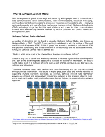
Software Defined Radio HandbookSamplingNyquist’s Theorem and SamplingA Simple TTechniqueechnique to Visualize SamplingBefore we look at SDR and its various implementations in embedded systems, we’ll review a theoremfundamental to sampled data systems such as thoseencountered in Software-Defined t’s Theorem:“Any signal can be represented by discretesamples if the sampling frequency is at least twicethe bandwidth of the signal.”Zone 1Zone 2Zone 3Zone 4Zone 5Zone 6Zone 7Figure 1Notice that we highlighted the word bandwidthrather than frequency. In what follows, we’ll attempt toshow the implications of this theorem and the correctinterpretation of sampling frequency, also known assampling rate.To visualize what happens in sampling, imaginethat you are using transparent “fan-fold” computerpaper. Use the horizontal edge of the paper as thefrequency axis and scale it so that the paper folds lineup with integer multiples of one-half of the samplingfrequency ƒs. Each sheet of paper now represent what wewill call a “Nyquist Zone”, as shown in Figure 1.3Pentek, Inc. One Park Way, Upper Saddle River, NJ 07458 Tel: (201) 818-5900 Fax: (201) 818-5904 Email: info@pentek.com http://www.pentek.com
Software Defined Radio HandbookSamplingSampling y0Baseband Sampling2fs5fs/23fs7fs/2No Signal EnergyZone 1Zone 2Zone 3Zone 4Zone 5Zone 6Zone 7Zone 1Figure 20Zone 3Zone 4Zone 5Zone 6Zone 7Figure 4Use the vertical axis of the fan-fold paper for signalenergy and plot the frequency spectrum of the signal tobe sampled, as shown in Figure 2. To see the effects ofsampling, collapse the transparent fan-fold paper into astack.Folded SignalsFall On Top ofEach OtherZone 2A baseband signal has frequency components thatstart at ƒ 0 and extend up to some maximum frequency.To prevent data destruction when sampling a basebandsignal, make sure that all the signal energy falls ONLY inthe 1st Nyquist band, as shown in Figure 4.There are two ways to do this:1. Insert a lowpass filter to eliminate all signalsabove ƒs /2, or2. Increase the sampling frequency so all signalspresent fall below ƒs /2.fs/2Note that ƒs/2 is also known as the “folding frequency”.Sampling Bandpass SignalsLet’s consider bandpass signals like the IF frequencyof a communications receiver that might have a 70 MHzcenter frequency and 10 MHz bandwidth. In this case,the IF signal contains signal energery from 65 to 75 MHz.Figure 3The resulting spectrum can be seen by holding thetransparent stack up to a light and looking through it.You can see that signals on all of the sheets or zones are“folded” or “aliased” on top of each other — and theycan no longer be separated.If we follow the baseband sampling rules above, wemust sample this signal at twice the highest signalfrequency, meaning a sample rate of at least 150 MHz.However, by taking advantage of a technique called“undersampling”, we can use a much lower sampling rate.Once this folding or aliasing occurs during sampling,the resulting sampled data is corrupted and can never berecovered. The term “aliasing” is appropriate becauseafter sampling, a signal from one of the higher zonesnow appears to be at a different frequency.4Pentek, Inc. One Park Way, Upper Saddle River, NJ 07458 Tel: (201) 818-5900 Fax: (201) 818-5904 Email: info@pentek.com http://www.pentek.com
Software Defined Radio o Signal EnergyZone 1Zone 23fsFolded signalsstill fall on top ofeach other - butnow there isenergy inonly one sheet !7fs/20fs/2No Signal EnergyZone 3Zone 4Zone 5Zone 6Zone 7Figure 5Figure 6Undersampling allows us to use aliasing to ouradvantage, providing we follow the strict rules of theNyquist Theorem.The major rule to follow for successful undersamplingis to make sure all of the energy falls entirely in oneNyquist zone.In our previous IF signal example, suppose we try asampling rate of 40 MHz.There two ways to do this:1. Insert a bandpass filter to eliminate all signalsoutside the one Nyquist zone.2. Increase the sampling frequency so all signalsfall entirely within one Nyquist zone.Figure 5 shows a fan-fold paper plot with Fs 40 MHz.You can see that zone 4 extends from 60 MHz to 80 MHz,nicely containing the entire IF signal band of 65 to 75 MHz.Now when you collapse the fan fold sheets as shownin Figure 6, you can see that the IF signal is preservedafter sampling because we have no signal energy in anyother zone.SummarySummaryBaseband sampling requires the sample frequency tobe at least twice the signal bandwidth. This is the sameas saying that all of the signals fall within the firstNyquist zone.Also note that the odd zones fold with the lowerfrequency at the left (normal spectrum) and the evenzones fold with the lower frequency at the right (reversedspectrum).In real life, a good rule of thumb is to use the 80%relationship:In this case, the signals from zone 4 are frequencyreversed. This is usually very easy to accommodate inthe following stages of SDR systems.Bandwidth 0.8 x ƒs/2Undersampling allows a lower sample rate even thoughsignal frequencies are high, PROVIDED all of thesignal energy falls within one Nyquist zone.To repeat the Nyquist theorem: The sampling frequencymust be at least twice the signal bandwidth — not thesignal frequency.5Pentek, Inc. One Park Way, Upper Saddle River, NJ 07458 Tel: (201) 818-5900 Fax: (201) 818-5904 Email: info@pentek.com http://www.pentek.com
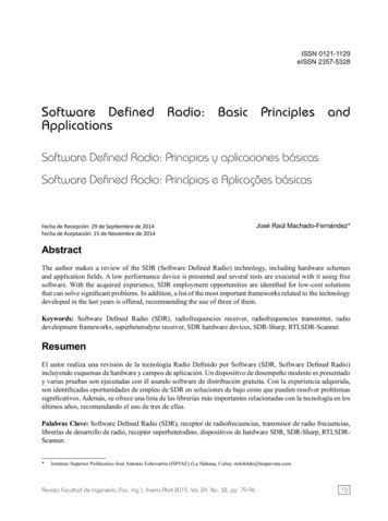
Software Defined Radio HandbookPrinciples of SDRAnalog Radio Receiver Block DiagramRadioReceiverAnalog Radio Receiver MixerRadioReceiverRF INPUT SIGNALFROM ANTENNASPEAKERANTENNAMIXER TRANSLATESINPUT SIGNAL BANDto IF FREQUENCYANALOGMIXERRFAMPIF OG LOCALOSCILLATORANALOGLOCALOSCILLATOR0FIFFRFFigure 8Figure 7The conventional heterodyne radio receiver shownin Figure 7, has been in use for nearly a century. Let’sreview the structure of the analog receiver so comparisonto a digital receiver becomes apparent.The mixer performs an analog multiplication of thetwo inputs and generates a difference frequency signal.The frequency of the local oscillator is set so that thedifference between the local oscillator frequency and thedesired input signal (the radio station you want toreceive) equals the IF.First the RF signal from the antenna is amplified,typically with a tuned RF stage that amplifies a regionof the frequency band of interest.For example, if you wanted to receive an FMstation at 100.7 MHz and the IF is 10.7 MHz, you wouldtune the local oscillator to:This amplified RF signal is then fed into a mixerstage. The other input to the mixer comes from the localoscillator whose frequency is determined by the tuningcontrol of the radio.100.7 - 10.7 90 MHzThis is called “downconversion” or “translation”because a signal at a high frequency is shifted down to alower frequency by the mixer.The mixer translates the desired input signal to theIF (Intermediate Frequency) as shown in Figure 8.The IF stage is a bandpass amplifier that only letsone signal or radio station through. Common centerfrequencies for IF stages are 455 kHz and 10.7 MHzfor commercial AM and FM broadcasts.The IF stage acts as a narrowband filter which onlypasses a “slice” of the translated RF input. The bandwidth of the IF stage is equal to the bandwidth of thesignal (or the “radio station”) that you are trying toreceive.The demodulator recovers the original modulatingsignal from the IF output using one of several differentschemes.For commercial FM, the bandwidth is about100 kHz and for AM it is about 5 kHz. This is consistent with channel spacings of 200 kHz and 10 kHz,respectively.For example, AM uses an envelope detector and FMuses a frequency discriminator. In a typical home radio,the demodulated output is fed to an audio power amplifierwhich drives a speaker.6Pentek, Inc. One Park Way, Upper Saddle River, NJ 07458 Tel: (201) 818-5900 Fax: (201) 818-5904 Email: info@pentek.com http://www.pentek.com
Software Defined Radio HandbookPrinciples of SDRSDR Receiver Block DiagramReceiverDDCDigital DownconverterAnalogRF SignalRFTUNERAnalogIF SignalA/DCONVDigital FILTERDSPDIGITALLOCALOSCFigure 9SDR Receiver MixerReceiverFigure 9 shows a block diagram of a softwaredefined radio receiver. The RF tuner converts analog RFsignals to analog IF frequencies, the same as the first threestages of the analog receiver.CHANNELBANDWIDTHThe A/D converter that follows digitizes the IF signalthereby converting it into digital samples. These samplesare fed to the next stage which is the digital downconverter(DDC) shown within the dotted lines.SignalMIXER TRANSLATESINPUT SIGNALBAND to DCIF BWDIGITAL LOCALOSCILLATORFLO FSIGThe digital downconverter is typically a singlemonolithic chip or FPGA IP, and it is a key part of theSDR system.0A conventional DDC has three major sections: A digital mixer A digital local oscillator An FIR lowpass filterFigure 10FSIGAt the output of the mixer, the high frequencywideband signals from the A/D input (shown in Figure10 above) have been translated down to DC as complex Iand Q components with a frequency shift equal to thelocal oscillator frequency.The digital mixer and local oscillator translate thedigital IF samples down to baseband. The FIR lowpassfilter limits the signal bandwidth and acts as a decimating lowpass filter. The digital downconverter includes alot of hardware multipliers, adders and shift registermemories to get the job done.This is similar to the analog receiver mixer exceptthere, the mixing was done down to an IF frequency.Here, the complex representation of the signal allows usto go right down to DC.The digital baseband samples are then fed to a blocklabeled DSP which performs tasks such as demodulation,decoding and other processing tasks.By tuning the local oscillator over its range, anyportion of the RF input signal can be mixed down to DC.Traditionally, these needs have been handled withdedicated application-specific ICs (ASICs), and programmable DSPs.In effect, the wideband RF signal spectrum can be“slid” around 0 Hz, left and right, simply by tuning thelocal oscillator. Note that upper and lower sidebands arepreserved.7Pentek, Inc. One Park Way, Upper Saddle River, NJ 07458 Tel: (201) 818-5900 Fax: (201) 818-5904 Email: info@pentek.com http://www.pentek.com
Software Defined Radio HandbookPrinciples of SDRDDC LLocalocal Oscillator and DecimationDDC Signal PProcessingrocessingTranslationA/DCONV90ODigital BasebandSamplesDIGITALLOCALOSCTuning FreqF1F2DecimationF3Figure 12Figure 11A Local Oscillator Frequency SwitchingThis process is called decimation and it means keepingone out of every N signal samples. If the decimatedoutput sample rate is kept higher than twice the outputbandwidth, no information is lost.A/D Sample Rate(before decimation)Sample Rate: FsDecimatedFilter OutputThe clear benefit is that decimated signals can beprocessed easier, can be transmitted at a lower rate, orstored in less memory. As a result, decimation candramatically reduce system costs!Sample Rate: Fs/NFigure 11B FIR Filter DecimationAs shown in Figure 12, the DDC performs twosignal processing operations:Because the local oscillator uses a digital phaseaccumulator, it has some very nice features. It switchesbetween frequencies with phase continuity, so you cangenerate FSK signals or sweeps very precisely with notransients as shown in Figure 11A.1. Frequency translation with the tuning controlledby the local oscillator.2. Lowpass filtering with the bandwidth controlledby the decimation setting.The frequency accuracy and stability are determinedentirely by the A/D clock so it’s inherently synchronousto the sampling frequency. There is no aging, drift orcalibration since it’s implemented entirely with digital logic.We will next turn our attention to the SoftwareDefined Radio Transmitter.Since the output of the FIR filter is band-limited, theNyquist theorem allows us to lower the sample rate. Ifwe are keeping only one out of every N samples, as shownin Figure 11B above, we have dropped the sampling rateby a factor of N.8Pentek, Inc. One Park Way, Upper Saddle River, NJ 07458 Tel: (201) 818-5900 Fax: (201) 818-5904 Email: info@pentek.com http://www.pentek.com
Software Defined Radio HandbookPrinciples of SDRSDR TTransmitterransmitter Block RFs/NDigitalBasebandSamples DIGITALDigital IFSamplesMIXERFsFsDUCDigital gRFSignalPowerAmplifierDIGITALLOCALOSCFigure 13DUC Signal PProcessingrocessingThe input to the transmit side of an SDR system isa digital baseband signal, typically generated by a DSPstage as shown in Figure 13 above.The digital hardware block in the dotted lines is aDUC (digital upconverter) that translates the basebandsignal to the IF frequency.DigitalBasebandSamplesFs/NThe D/A converter that follows converts the digitalIF samples into the analog IF signal.INTERPOLATIONFILTERDigitalBasebandSamples DIGITALMIXERFsDUCDigital UpConverterNext, the RF upconverter converts the analog IFsignal to RF frequencies.Digital IFSamplesFsDIGITALLOCALOSCFigure 14Finally, the power amplifier boosts signal energy tothe antenna.Inside the DUC shown in Figure 14, the digitalmixer and local oscillator at the right translate basebandsamples up to the IF frequency. The IF translationfrequency is determined by the local oscillator.The mixer generates one output sample for each ofits two input samples. And, the sample frequency atthe mixer output must be equal to the D/A samplefrequency ƒs .Therefore, the local oscillator sample rate and thebaseband sample rate must be equal to the D/A samplefrequency ƒs .The local oscillator already operates at a sample rateof ƒs , but the input baseband sample frequency at theleft is usually much lower. This problem is solved withthe Interpolation Filter.9Pentek, Inc. One Park Way, Upper Saddle River, NJ 07458 Tel: (201) 818-5900 Fax: (201) 818-5904 Email: info@pentek.com http://www.pentek.com
Software Defined Radio HandbookPrinciples of SDRInterpolation FFilter:ilter: Time domainFs/NIQInterpolation FFilter:ilter: FFrequencyrequency DomainFsINTERPOLATINGLOW PASSFIR FILTERFsDUCDigital IONFACTOR NINTERPOLATEDBASEBAND INPUTBaseband InputDigital IFSamplesTRANSLATED OUTPUTMIXERSample Rate: Fs/NLOCALOSCILLATORF IF FreqInterpolatingFilter OutputSample Rate: Fs0Figure 15IF FreqFigure 16Figure 16 is a frequency domain view of the digitalupconversion process.The interpolation filter must boost the basebandinput sample frequency of ƒs /N up to the required mixerinput and D/A output sample frequency of ƒs .This is exactly the opposite of the frequency domainview of the DDC in Figure 10.The interpolation filter increases the sample frequencyof the baseband input signal by a factor N, known asthe interpolation factor.The local oscillator setting is set equal to therequired IF signal frequency, just as with the DDC.At the bottom of Figure 15, the effect of theinterpolation filter is shown in the time domain.Notice the baseband signal frequency content iscompletely preserved by filling in additional samples inthe spaces between the original input samples.The signal processing operation performed by theinterpolation filter is the inverse of the decimation filterwe discussed previously in the DDC section.10Pentek, Inc. One Park Way, Upper Saddle River, NJ 07458 Tel: (201) 818-5900 Fax: (201) 818-5904 Email: info@pentek.com http://www.pentek.com
Software Defined Radio HandbookPrinciples of SDRDDC PProcessingrocessingA/DCONVDUC INTERPOLATEFILTERDIGITALMIXERD/ACONVFs N NDeci mationInter polationBandwidthBandwidthFreq uencyTuningDSPFilteringDIGITALLOCALOSCFreq uencyTuningFigure 18Figure 17Figure 17 shows the two-step processing performedby the digital downconverter.Figure 18 shows the two-step processing performedby the digital upconverter:Frequency translation from IF down to baseband isperformed by the local oscillator and mixer.The ratio between the required output sample rateand the sample rate input baseband sample rate determines the interpolation factor N.The “tuning knob” represents the programmabilityof the local oscillator frequency to select the desiredsignal for downconversion to baseband.The baseband signal bandwidth is set by settingdecimation factor N and the lowpass FIR filter: Baseband sample frequency ƒb ƒs /N Baseband bandwidth 0.8 x ƒb Baseband bandwidth 0.8 x ƒb Output sample frequency ƒs ƒb x NAgain, the bandwidth equation assumes a complex(I Q) baseband input and an 80% filter.The “bandwidth knob” represents the programmability of the interpolation factor to select the desiredinput baseband signal bandwidth.The baseband bandwidth equation reflects a typical80% passband characteristic, and complex (I Q) samples.Frequency translation from baseband up to IF isperformed by the local oscillator and mixer.The “bandwidth knob” represents the programmability of the decimation factor to select the desiredbaseband signal bandwidth.The “tuning knob” represents the programmabilityof the local oscillator frequency to select the desired IFfrequency for translation up from baseband.11Pentek, Inc. One Park Way, Upper Saddle River, NJ 07458 Tel: (201) 818-5900 Fax: (201) 818-5904 Email: info@pentek.com http://www.pentek.com
Software Defined Radio HandbookPrinciples of SDRKey DDC and DUC BenefitsA/DCONVDigital IFSamplesDIGITALMIXERSDR ATIONFILTERDUCDigital DownConverterDigitalBasebandSamples DIGITALMIXERFsDUCDigital UpConverterDigital IFSamplesFsD/ACONVDIGITALLOCALOSCFigure 19Figure 20Think of the DDC as a hardware preprocessor forprogrammable DSP or GPP processor. It preselects onlythe signals you are interested in and removes all others.This provides an optimum bandwidth and minimumsampling rate into the processor.Here we’ve ranked some of the popular signalprocessing tasks associated with SDR systems on a twoaxis graph, with computational Processing Intensity onthe vertical axis and Flexibility on the horizontal axis.What we mean by process intensity is the degree ofhighly-repetitive and rather primitive operations. At theupper left, are dedicated functions like A/D convertersand DDCs that require specialized hardware structuresto complete the operations in real time. ASICs are usuallychosen for these functions.The same applies to the DUC. The processor onlyneeds to generate and deliver the baseband signalssampled at the baseband sample rate. The DUC thenboosts the sampling rate in the interpolation filter,performs digital frequency translation, and deliverssamples to the D/A at a very high sample rate.Flexibility pertains to the uniqueness or variabilityof the processing and how likely the function may haveto be changed or customized for any specific application.At the lower right are tasks like analysis and decisionmaking which are highly variable and often subjective.The number of processors required in a system isdirectly proportional to the sampling frequency ofinput and output data. As a result, by reducing thesampling frequency, you can dramatically reduce thecost and complexity of the programmable DSPs orGPPs in your system.Programmable general-purpose processors or DSPsare usually chosen for these tasks since these tasks can beeasily changed by software.Not only do DDCs and DUCs reduce the processorworkload, the reduction of bandwidth and sampling ratehelps save time in data transfers to another subsystem. Thishelps minimize recording time and disk space, and reducestraffic and bandwidth across communication channels.Now let’s temporarily step away from the softwareradio tasks and take a deeper look at programmablelogic devices.12Pentek, Inc. One Park Way, Upper Saddle River, NJ 07458 Tel: (201) 818-5900 Fax: (201) 818-5904 Email: info@pentek.com http://www.pentek.com
Software Defined Radio HandbookTechnologyEarly Roles for FPGAsRolesLegacy FPGA Design Methodologies§ Tools were oriented to hardware engineers§ Used primarily to replace discrete digitalhardware circuitry for: Schematic processors Boolean processors Gates, registers, counters, multipliers Control logic Glue logic§ Successful designs required high-levelhardware engineering skills for: Registers and gates State machines Counters and dividers§ Devices were selected by hardware engineers§ Programmed functions were seldom changedafter the design went into productionFigure 21Critical paths and propagation delaysPin assignment and pin lockingSignal loading and drive capabilitiesClock distributionInput signal synchronization and skew analysisFigure 22As true programmable gate functions becameavailable in the 1970’s, they were used extensively byhardware engineers to replace control logic, registers,gates, and state machines which otherwise would haverequired many discrete, dedicated ICs.These programmable logic devices were mostly thedomain of hardware engineers and the software toolswere tailored to meet their needs. You had tools foraccepting boolean equations or even schematics to helpgenerate the interconnect pattern for the growingnumber of gates.Often these programmable logic devices were onetime factory-programmed parts that were soldered downand never changed after the design went into production.Then, programmable logic vendors started offeringpredefined logic blocks for flip-flops, registers andcounters that gave the engineer a leg up on popularhardware functions.Nevertheless, the hardware engineer was stillintimately involved with testing and evaluating thedesign using the same skills he needed for testingdiscrete logic designs. He had to worry about propagation delays, loading, clocking and synchronizing—alltricky problems that usually had to be solved the hardway—with oscilloscopes or logic analyzers.13Pentek, Inc. One Park Way, Upper Saddle River, NJ 07458 Tel: (201) 818-5900 Fax: (201) 818-5904 Email: info@pentek.com http://www.pentek.com
Software Defined Radio HandbookTechnologyFPGAs: New Device TTechnologyechnologyFPGAs: New Development TToolsoolsu500 MHz DSP Slices and Memory StructuresOver 3500 dedicated on-chip hardware multipliersu On-board GHz Serial TransceiversuPartial Reconfigurability Maintainsu Operation During Changesu Switched Fabric Interface Enginesu Over 690,000 Logic Cellsu Gigabit Ethernet media access controllersu On-chip 405 PowerPC RISC micro-controller coresu Memory densities approaching 85 million bitsu Reduced power with core voltages at 1 voltu Silicon geometries to 28 nanometersu High-density BGA and flip-chip packagingu Over 1200 user I/O pinsuu§ High Level Design Tools Block Diagram System Generators Schematic Processors High-level language compilers forVHDL & Verilog Advanced simulation tools for modeling speed,propagation delays, skew and board layout Faster compilers and simulators save time Graphically-oriented debugging tools§ IP (Intellectual Property) Cores FPGA vendors offer both free and licensed cores FPGA vendors promote third party core vendors Wide range of IP cores availableConfigurable logic and I/O interface standardsFigure 24Figure 23To support such powerful devices, new design toolsare appearing that now open up FPGAs to both hardware and software engineers. Instead of just acceptinglogic equations and schematics, these new tools acceptentire block diagrams as well as VHDL and Verilogdefinitions.It’s virtually impossible to keep up to date on FPGAtechnology, since new advancements are being madeevery day.The hottest features are processor cores inside thechip, computation clocks to 500 MHz and above, andlower core voltages to keep power and heat down.Choosing the best FPGA vendor often hingesheavily on the quality of the design tools available tosupport the parts.Several years ago, dedicated hardware multipliersstarted appearing and now you’ll find literally thousandsof them on-chip as part of the DSP initiative launchedby virtually all FPGA vendors.Excellent simulation and modeling tools help toquickly analyze worst case propagation delays andsuggest alternate routing strategies to minimize themwithin the part. This minimizes some of the trickytiming work for hardware engineers and can save onehours of tedious troubleshooting during design verification and production testing.High memory densities coupled with very flexiblememory structures meet a wide range of data flowstrategies. Logic slices with the equivalent of over tenmillion gates result from silicon geometries shrinkingbelow 0.1 micron.BGA and flip-chip packages provide plenty of I/Opins to support on-board gigabit serial transceivers andother user-configurable system interfaces.In the last few years, a new industry of third partyIP (Intellectual Property) core vendors now offerthousands of application-specific algorithms. These areready to drop into the FPGA design process to help beatthe time-to-market crunch and to minimize risk.New announcements seem to be coming out everyday from chip vendors like Xilinx and Altera in a neverending game of outperforming the competition.14Pentek, Inc. One Park Way, Upper Saddle River, NJ 07458 Tel: (201) 818-5900 Fax: (201) 818-5904 Email: info@pentek.com http://www.pentek.com
Software Defined Radio HandbookTechnologyFPGAs for SDRFPGAs Bridge the SDR Application Space§ Parallel Processing§ Hardware Multipliers for DSP FPGAs can now have over 500 hardware multipliers§ Flexible Memory Structures Dual port RAM, FIFOs, shift registers, look up tables, etc.§ Parallel and Pipelined Data Flow Systolic simultaneous data movement§ Flexible I/O Supports a variety of devices, buses and interface standards§ High Speed§ Available IP cores optimized for special functionsFigure 26Figure 25Like ASICs, all the logic elements in FPGAs canexecute in parallel. This includes the hardware multipliers, and you can now get over 1000 of them on a singleFPGA.As a result, FPGAs have significantly invaded theapplication task space as shown by the center bubble inthe task diagram above.This is in sharp contrast to programmable DSPs,which normally have just a handful of multipliers thatmust be operated sequentially.They offer the advantages of parallel hardware tohandle some of the high process-intensity functions likeDDCs and the benefit of programmability to accommodate some of the decoding and analysis functions of DSPs.FPGA memory can now be configured with thedesign tool to implement just the right structure fortasks that include dual port RAM, FIFOs, shift registersand other popular memory types.These advantages may come at the expense ofincreased power dissipation and increased product costs.However, these considerations are often secondary to theperformance and capabilities of these remarkable devices.These memories can be distributed along the signalpath or interspersed with the multipliers and mathblocks, so that the whole signal processing task operatesin parallel in a systolic pipelined fashion.Again, this is dramatically different from sequentialexecution and data fetches from external memory as in aprogrammable DSP.As we said, FPGAs now have specialized serial andpar
Software Defined Radio Handbook Figure 7 The conventional heterodyne radio receiver shown in Figure 7, has been in use for nearly a century. Let’s review the structure of the analog receiver so comparison to a digital receiver becomes apparent. First the RF signal from the antenna is amplified, typically with a tuned RF stage that amplifies a .