Transcription
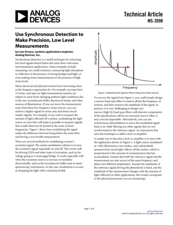
Technical ArticleMS-2698Use Synchronous Detection toMake Precision, Low LevelMeasurementsby Luis Orozco, systems applications engineer,Analog Devices, Inc.Synchronous detection is a useful technique for extractinglow level signals buried below the noise floor with manyinstrumentation applications. Some examples includemeasuring very small resistance, measuring light absorptionor reflection in the presence of strong background light, oreven making strain measurements in the presence of highnoise levels.Many electrical and physical systems have increasing noiseas the frequency approaches dc. For example, op amps have1/f noise, and open air light measurement systems aresubject to noise from changing ambient light conditions dueto the sun, incandescent bulbs, fluorescent lamps, and othersources of illumination. If you can move the measurementaway from these low frequency noise sources, you canachieve a higher signal-to-noise ratio and detect muchweaker signals. For example, if you wish to measure theamount of light reflected off a surface, modulating the lightsource at a few kHz will make it possible to measure signalsthat would otherwise be buried in the noise at lowerfrequencies. Figure 1 shows how modulating the signalmakes the difference between being below the noise floorand having a recoverable measurement.Figure 1. Modulating the Signal to Move It Away from Noise SourcesTo recover the signal from Figure 1, you could simply designa narrow band-pass filter to remove all but the frequency ofinterest, and then measure the amplitude of the signal. Inpractice, it is very challenging to design verynarrow (high Q) band-pass filters with discrete components.If the specifications call for an extremely narrow filter, itmay even be impossible. Alternatively, you can usesynchronous demodulation to move the modulated signalback to dc while filtering out other signals that are notsynchronized to the reference signal. An instrument thatuses this technique is called a lock-in amplifier.A simple way to describe a lock-in amplifier is to start withthe application shown in Figure 2. A light source modulatedat 1 kHz illuminates a test surface, and a photodiodemeasures how much light reflects off the surface, which isproportional to the amount of contamination that hasaccumulated. Assume that both the reference signal and themeasurement are sine waves (of the same frequency andphase, but different amplitudes). Assume the amplitude ofthe reference signal driving the photodiode is fixed, and theamplitude of the measurement changes with the amount oflight reflected (in other applications, this would correspondto the physical parameter you are measuring).There are several methods for modulating a sensor’sexcitation signal. The easiest modulation scheme is to turnthe excitation signal repeatedly on and off. This works wellfor driving LEDs and other types of excitation, such as thevoltage going to a strain gage bridge. It works especially wellwhen the excitation source is not easy to modulateelectronically, such as the incandescent bulbs used in manyspectroscopy instruments. In this case, modulation is as easyas chopping the light with a mechanical disk.Page 1 of 8www.analog.com@2014 Analog Devices, Inc. All rights reserved.
Technical ArticleMS-2698The result of multiplying two sine waves together is a signalwith frequency components at the sum and difference of thetwo input sine waves. In this case, the two sine waves have thesame frequency, and Equation 1 shows how the result is onesignal at dc and another at twice the original frequency (thenegative sign indicates it has 180 of phase shift). A low-passfilter removes everything but the dc component of the signal.consider a noisy input signal. The output of themultiplication stage will still result in only the signal at themodulation frequency moving back to dc, with all otherfrequency components moving to other, non-dcfrequencies. For example, Figure 3 depicts a system withstrong noise sources at 50 Hz and 2.5 kHz, and a very weaksignal of interest modulated with a sine wave at 1 kHz.The advantage of using this technique is more evident if you𝐴𝑠𝑖𝑛(2𝜋𝑓𝑚 𝑡) 𝐵 𝑠𝑖𝑛(2𝜋𝑓𝑚 𝑡) 12111𝐴𝐵 𝑐𝑜𝑠(2𝜋 (𝑓𝑚 𝑓𝑚 ) 𝑡) 𝐴𝐵 𝑐𝑜𝑠(2𝜋 (𝑓𝑚 𝑓𝑚 ) 𝑡)221𝐴𝐵 𝐴𝐵𝑐𝑜𝑠(2𝜋2𝑓𝑚 𝑡)2(Equation 1)The result of multiplying the input with the reference is asignal at dc, and other signals at 950 Hz, 1.05 kHz, 1.5 kHz,2 kHz, and 3.5 kHz. The dc signal contains the desiredinformation, so you can use a low-pass filter to remove all ofthe other frequencies.Figure 2. Measuring Surface Contamination with a Lock-In AmplifierFigure 3. Synchronous Demodulation Picks Out a Weak, 1 kHz Signal in the Presence of Strong Noise Sources at 50 Hz and 2.5kHz Page 2 of 8
Technical ArticleMS-2698Using a square wave-based lock-in amplifier requires asimple circuit, but its noise rejection performance is inferiorto a system using sine waves. Figure 5 shows the frequencydomain representation of using a square wave as the sensorexcitation and reference signal. A square wave is made up ofan infinite sum of sine waves at the fundamental and all oddharmonics. Multiplying two square waves of the samefrequency involves multiplying each sine component of thereference times each sine component of the measured signal.The result is a dc signal that contains energy from everyharmonic of the square wave. Any unwanted signals thatappear at any odd harmonic frequency will not be filteredout (although it will be scaled down depending on whichharmonic it falls in). When designing a square wave-basedlock-in amplifier, it is important to pick a modulationfrequency with harmonics that are not at any frequency orharmonics of known noise sources. For example, instead ofpicking a 1 kHz modulation frequency (the 20th harmonic of50 Hz), pick 1.0375 kHz, which does not coincide withharmonics of 50 Hz or 60 Hz.Any noise components that are close to the signal of interestwill appear at frequencies close to dc, so it is important topick a modulation frequency that does not have strong noisesources near it. If this is not possible, then you will need alow-pass filter with a very low cutoff frequency and sharpresponse, at the expense of a long settling time.PRACTICAL LOCK-IN IMPLEMENTATIONSGenerating a sine wave to modulate the signal source can beimpractical, and some systems use a square wave instead.Generating a square wave excitation is much simpler thangenerating a sine wave, because it can be done withsomething as simple as a microcontroller pin that toggles ananalog switch or a MOSFET.The circuit of Figure 4 is an easy way to implement ahardware-based lock-in amplifier. A microcontroller orother digital device generates a square wave excitation signalthat causes the sensor to respond. In the case of aphotodiode, the first amplifier would be a current-to-voltageconverter, while a strain gage bridge would require aninstrumentation amplifier.Even with this drawback, the circuit is simple and low cost.Using a low noise amplifier and picking the rightmodulation frequency can still result in a greatimprovement over trying to make a dc measurement.The same signal that excites the sensor controls the ADG619SPDT switch. When the excitation signal is positive, theADG619 configures the amplifier for a gain of 1. When theexcitation is negative, the ADG619 configures the amplifierfor a gain of –1, which essentially “flips” the negative side ofthe square wave. This is mathematically equivalent tomultiplying the measured signal times the reference squarewave. The output RC filter removes any signals at otherfrequencies, and the output voltage is a dc signal equal tohalf the peak-to-peak voltage of the measured square wave.Figure 5. If the Input Signal (A) and the Reference (B) Are Both Square Waves,Multiplying Them Together (C) Effectively Demodulates Every Harmonic ofthe Input SignalA SIMPLE, INTEGRATED ALTERNATIVEThe circuit of Figure 4 requires an op amp, analog switch,and some discrete components, plus a reference clock froma microcontroller. An alternative to this circuit is to use anintegrated synchronous demodulator like the ADA2200.Figure 6 shows the internal blocks of the ADA2200, whichinclude a buffered input, a programmable IIR filter, and amultiplier. It also includes a block that shifts the referencesignal by 90 , which makes it easy to measure or compensatefor phase shifts between the reference clock and input signal.Figure 4. Lock-In Amplifier Using Square Wave ExcitationAlthough the circuit is simple, it is important to pick theright op amp for the job. The input ac coupling stageremoves most of the input noise at low frequencies, but any1/f noise and offset error from the last amplifier are notfiltered out. The ADA4077-1 has 250 nV p-p of noise from0.1 Hz to 10 Hz and 0.55 µV/ C of offset drift, making it anideal candidate for this application.Page 3 of 8
Technical ArticleMS-2698The benefits of this operation are explained in detail in thefollowing section.Figure 8. Using a Sine Wave as the Reference Signal Prevents Noise fromDemodulating to DCFigure 6. ADA2200 Internal ArchitectureOne additional difficulty is that if there is any phase shiftbetween the reference signal and the measured signal, theresult of multiplying the two together will result in a loweramplitude output than if they were perfectly in phase. Thiscan occur if the sensor signal conditioning circuit includesany filters (which introduce phase delay). With an analoglock-in amplifier, the only way to address this is to includeadditional phase compensation circuits in the referencesignal path. This is not trivial, because the circuit needs to beadjustable to compensate for different phase delays, and willvary with temperature, component tolerance, etc. An easieralternative is to add a second multiplication stage thatmultiplies the measured signal with a 90 phase shiftedversion of the reference. The result of this second stage willbe a signal proportional to the out of phase component ofthe input. Figure 9 shows this concept.Implementing a lock-in detection circuit with the ADA2200simply requires applying a clock frequency that is 64 timesthe desired reference frequency. The default configurationof the programmable filter is for a band-pass response,removing the need to ac couple the signal as in the circuit ofFigure 4. The ADA2200’s sampled analog output willgenerate images around multiples of the sampling rate. Youcan use an RC filter followed by a Σ-Δ ADC to remove theseimages and measure only the demodulated dc component ofthe signal.The outputs of the low-pass filters after the two multiplierstages are low frequency signals proportional to the in-phase(I) and quadrature (Q) components of the input. Tocalculate the magnitude of the input signal, simply take thesum of the squares of the I and Q outputs. An additionalbenefit of this architecture is that you can also calculate thephase between the excitation/reference signal and the input.Figure 7. Lock-In Amplifier Implementation with the ADA2200IMPROVING THE SQUARE WAVE LOCK-IN CIRCUITFigure 8 shows an improvement to a square wave modulatedcircuit. If you excite the sensor with a square wave, but nowmultiply the measured signal with a sine wave of the samefrequency and phase, only the signal content at thefundamental frequency will move to dc, while all of theother harmonics will move to non-dc frequencies. Thismakes it easy to use a low-pass filter and eliminateeverything but the dc component of the measured signal.Page 4 of 8
Technical ArticleMS-2698a sine wave of the same frequency and phase as the inputreference. One caveat of this approach is that the internallygenerated sine wave must have low distortion.Although this system could be implemented using a discretePLL and multipliers, using an FPGA to implement the lockin amplifier functions results in several performance benefits.Figure 11 shows a lock-in amplifier built with an FPGA usinga front end based on the ADA4528-1 zero-drift amplifier andan AD7175 24-bit Σ-Δ ADC. An application like this doesnot need very high bandwidth, so we can set the lock-inamplifier’s equivalent noise bandwidth to 50 Hz. The deviceunder test is again any sensor that can be excited externally.The ADA4528-1 is configured with a noise gain of 20 to takeadvantage of the full scale range of the ADCFigure 9. Using a Quadrature Version of the Reference Signal to CalculateMagnitude and PhaseAll of the systems discussed so far generate a referencesignal that excites a sensor. One final refinement to the lock-Figure 10. Using a PLL to Lock on to an External Reference Signalin amplifier is to allow an external signal to act as areference. For example, Figure 10 shows a system that uses abroadband incandescent light to test the optical propertiesof a surface. A system like this can measure parameters suchas the reflectivity of mirrors, or the amount ofcontamination on a surface. It is much simpler to use amechanical chopper disk to modulate an incandescentsource than to apply electronic modulation. A cheapposition sensor close to the chopper disk generates a squarewave reference signal to feed the lock-in amplifier. Ratherthan using this signal directly, a phase-locked loop generates(arbitrarily set for this example). Although dc errors do notaffect the measurement, it is still important to minimizeoffset drift and 1/f noise because they will decrease theavailable dynamic range, especially when the amplifier isconfigured for high gain. The ADA4528-1’s 2.5 µV of worstcase input offset error represents only 10 ppm of theAD7175’s full scale input range (with a 2.5 V reference). Thedigital high-pass filter after the ADC removes any dc offsetand very low frequency noise. To calculate the output noise,we need to know the voltage noise density of the AD7175.The data sheet specifies the ADC noise at 5.9 µV rms with anPage 5 of 8
Technical ArticleMS-2698other unwanted signals present at the harmonic frequencies,just like when two square waves are multiplied together (seeFigure 5). One advantage of generating this reference sinewave digitally is that it is relatively easy to generate a verylow distortion signal simply by adjusting the numberprecision. For example, Figure 12 shows four digitallygenerated sine waves using 4-, 8-, 16-, and 32-bit precision.Obviously, using 4-bit precision results in performance notmuch different from the case in Figure 5, but the situationquickly improves by using higher precision numbers. At16 bits of precision, it would take some effort to generate ananalog signal with such low total harmonic distortion(THD), and at 32 bits, where the THD is over –200 dB, itwould be impossible to match with an analog circuit. Inaddition, because these are digitally generated signals, theyare perfectly repeatable. Once the data has been converted tothe digital domain and enters the FPGA, there is noadditional noise or drift to take into account.output data rate of 50 kSPS, using the Sinc5 Sinc1 filterand with the input buffer enabled. The equivalent noisebandwidth with these settings is 21.7 kHz, which results in avoltage noise density of 40 nV/ Hz. The broadband inputnoise of the ADA4528 is 5.9 nV/ Hz, which appears at theoutput as 118 nV/ Hz resulting in a combined noise densityof 125 nV/ Hz. Since the digital filter has an equivalent noisebandwidth of only 50 Hz, the output noise is 881 nVrms.With a 2.5 V input range, this results in a system with126 dB of dynamic range. We can trade off bandwidth fordynamic range by adjusting the frequency response of thelow-pass filter. For example, setting the filters for anequivalent noise bandwidth of 1 Hz results in 143 dB ofdynamic range, and setting the bandwidth to 250 Hz resultsin 119 dB of dynamic range.After the multipliers, the low-pass filters remove any highfrequency components and output the in-phase andquadrature components of the signal. Continuing with theassumption that the equivalent noise bandwidth of thefilters is only 50 Hz, there is no reason to deliver data at theoriginal sampling rate of 250 kSPS. The low-pass filters caninclude a decimation stage to reduce the output data rate.The last step in the process is to calculate the magnitude andphase of the input signal from the in-phase and quadraturecomponents.Figure 11. FPGA-Based Lock-In AmplifierThe digital phase-locked loop generates a sine wave lockedto the excitation signal (which can be an external signal, orinternally generated in the FPGA, and does not have to be asine wave). Any harmonics in the reference sine wave willalso multiply with the input signal, demodulating noise andPage 6 of 8
Technical ArticleMS-2698Figure 12. Numerically Generated Sine Waves with Different Number Precisionattractive when compared with a simple dc measurement.An improvement from this circuit is to use a sine wavereference and a multiplier, but this can be challenging toimplement in the analog domain. For the ultimateperformance, consider using a low noise, high resolutionΣ-Δ ADC, such as the AD7175, to digitize the input signal,and then generate the reference sine wave, and all of theother elements of the lock-in amplifier in the digital domain.SUMMARYSmall, low frequency signals buried in the noise floor can bedifficult to measure, but applying modulation and lock-inamplifier techniques can result in high precisionmeasurements. In its simplest form, a lock-in amplifier canbe an op amp that switches between two gains. Althoughthis does not result in the lowest noise performance, thesimplicity and low cost of the circuit still make it veryPage 7 of 8
Technical ArticleMS-2698AUTHORLuis Orozco [luis.orozco@analog.com] is a systemapplications engineer in ADI’s industrial andinstrumentation segment. He focuses on precisioninstrumentation, chemical analysis, and environmentalmonitoring applications. Luis joined ADI in February 2011.Prior to joining ADI, he designed data acquisitionequipment for over 10 years.RESOURCESShare this article onOne Technology Way P.O. Box 9106 Norwood, MA 02062-9106, U.S.A.Tel: 781.329.4700 Fax: 781.461.3113 www.analog.comTrademarks and registered trademarks are the property of theirrespective owners.TA12671-0-9/14www.analog.com 2014 Analog Devices, Inc. All rights reserved.Page 8 of 8
lock-in amplifier, it is important to pick a modulation frequency with harmonics that are not at any frequency or harmonics of known noise sources. For example, instead of picking a 1 kHz modulation frequency (the 20. th. harmonic of 50 Hz), pick 1.0375 kHz,