Transcription
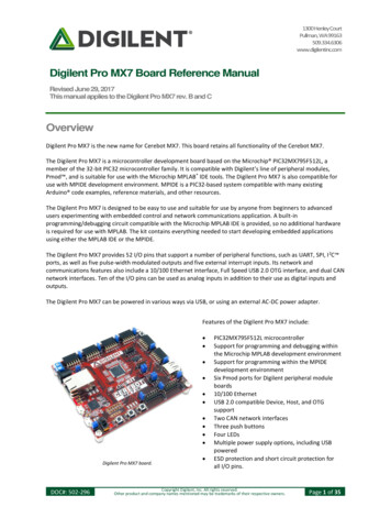
1300 Henley CourtPullman, WA 99163509.334.6306www.digilentinc.comDigilent Pro MX7 Board Reference ManualRevised June 29, 2017This manual applies to the Digilent Pro MX7 rev. B and COverviewDigilent Pro MX7 is the new name for Cerebot MX7. This board retains all functionality of the Cerebot MX7.The Digilent Pro MX7 is a microcontroller development board based on the Microchip PIC32MX795F512L, amember of the 32-bit PIC32 microcontroller family. It is compatible with Digilent's line of peripheral modules,Pmod , and is suitable for use with the Microchip MPLAB IDE tools. The Digilent Pro MX7 is also compatible foruse with MPIDE development environment. MPIDE is a PIC32-based system compatible with many existingArduino code examples, reference materials, and other resources.The Digilent Pro MX7 is designed to be easy to use and suitable for use by anyone from beginners to advancedusers experimenting with embedded control and network communications application. A built-inprogramming/debugging circuit compatible with the Microchip MPLAB IDE is provided, so no additional hardwareis required for use with MPLAB. The kit contains everything needed to start developing embedded applicationsusing either the MPLAB IDE or the MPIDE.The Digilent Pro MX7 provides 52 I/O pins that support a number of peripheral functions, such as UART, SPI, I 2C ports, as well as five pulse-width modulated outputs and five external interrupt inputs. Its network andcommunications features also include a 10/100 Ethernet interface, Full Speed USB 2.0 OTG interface, and dual CANnetwork interfaces. Ten of the I/O pins can be used as analog inputs in addition to their use as digital inputs andoutputs.The Digilent Pro MX7 can be powered in various ways via USB, or using an external AC-DC power adapter.Features of the Digilent Pro MX7 include: Digilent Pro MX7 board.DOC#: 502-296 PIC32MX795F512L microcontrollerSupport for programming and debugging withinthe Microchip MPLAB development environmentSupport for programming within the MPIDEdevelopment environmentSix Pmod ports for Digilent peripheral moduleboards10/100 EthernetUSB 2.0 compatible Device, Host, and OTGsupportTwo CAN network interfacesThree push buttonsFour LEDsMultiple power supply options, including USBpoweredESD protection and short circuit protection forall I/O pins.Copyright Digilent, Inc. All rights reserved.Other product and company names mentioned may be trademarks of their respective owners.Page 1 of 35
Digilent Pro MX7 Board Reference ManualFeatures of the PIC32MX795F512L include: Digilent Pro MX7 Circuit Diagram 512KB internal program flash memory128KB internal SRAM memoryUSB 2.0 compliant full-speed On-The-Go (OTG)controller with dedicated DMA channel10/100 Ethernet controllerTwo CAN network controllersUp to four serial peripheral interfaces (SPI)Up to six UART serial interfacesUp to four I2C serial interfacesFive 16-bit timer/countersFive timer capture inputsFive compare/PWM outputsSixteen 10-bit analog inputsTwo analog comparatorsFunctional DescriptionThe Digilent Pro MX7 is designed for embedded control and network communications applications as well asgeneral microprocessor experimentation. Firmware suitable for many applications can be downloaded to theDigilent Pro MX7’s programmable PIC32 microcontroller.The Digilent Pro MX7 has a number of input/output connection options, and is designed to work with the Digilentline of Pmods that provide various input and output functions. For more information, visit www.digilentinc.com. Inaddition to the Pmod ports, the board provides three push buttons and four LEDs for user I/O, as well as providingconnections for two I2C busses. A serial EEPROM is provided on one of the I 2C busses.The Digilent Pro MX7 features a flexible power supply system with a number of options for powering the board aswell as powering peripheral devices connected to the board. It can be USB powered via the debug USB port, theUSB UART serial port, or the USB device port. It can also be powered from an external 5V power supply.1Programming ToolsThe Digilent Pro MX7 can be used with either the Microchip MPLAB development environment or the MPIDEdevelopment environment. When used with the MPLAB \ IDE, in-system-programming and debugging of firmwarerunning on the PIC32MX795 microcontroller is supported using an on-board programming/debugging circuitlicensed from Microchip.The Digilent Pro MX7 is immediately useable with either the MPLAB IDE or the MPIDE. No additional hardware isrequired to use the board with the Microchip MPLAB tools.Copyright Digilent, Inc. All rights reserved.Other product and company names mentioned may be trademarks of their respective owners.Page 2 of 35
Digilent Pro MX7 Board Reference Manual1.1Using the Digilent Pro MX7 with Microchip Development ToolsThe Microchip MPLAB IDE or the MPLAB X IDE can be used to program and debug code running on the Digilent ProMX7 board using the built-in programming/debugging circuit.The MPLAB development environment can be downloaded from the Microchip website. This software suiteincludes a free evaluation copy of the Microchip C32 compiler for use with the PIC32 microcontroller family. Thelicensed debugger is compatible with the MPLAB IDE version 8.63 or later, or all versions of MPLAB X.When creating a new project, use the "Configure.Select Device " menu to specify the PIC32 device being used.Ensure that the device is set to PIC32MX795F512L.In order to use the on-board programming/debugging circuit, it must be selected as the debugger or programmerwithin the MPLAB IDE. Use the "Debugger.Select Tool" menu, or the "Programmer.Select Tool" menu, and select"Licensed Debugger" as the programmer or debugger.The licensed debugger interface uses USB connector J15, labeled DEBUG. Connector J15 is a USB micro-Bconnector located on the left side of the board below the Ethernet RJ45 connector. Use a USB-A to micro-B cable(provided with the board) to connect to an available USB port on the PC.When the licensed debugger is selected as the programming or debugging device, the MPLAB IDE will check theversion number of the firmware running on the debugger and offer to update if it is out of date with the version ofMPLAB being used.The PIC32 in-system programming/debugging interface uses two pins on the microcontroller. These devicessupport two alternate pin pairs for this interface: PGC1/PGD1 or PGC2/PGD2. The PGC2/PGD2 pair is used bydefault. Due to conflicting uses of the microcontroller pins, the Digilent Pro MX7 is designed to use the PGC1/PGD1pair of pins. Because of this, it is necessary to select the use of PGC1/PGD1 for the debugging interface. This isdone using configuration variables set using the #pragma config statement. The following statement must beused to configure the microcontroller for use with the on-board licensed debugger circuit:#pragma config ICESEL ICS PGx1The MPLAB IDE may report an error indicating that the device is not configured for debugging until a programcontaining this statement has been programmed into the board.The MCLR pin on the PIC32 microcontroller is used by the hardware programming/debugging interface to reset theprocessor. This same pin is used by the USB serial converter to reset the processor when using the MPIDE. It ispossible that the reset function from the USB serial interface can interfere with correct operation of the Microchipprogramming and debugging tools. If this happens, jumper JP11 can be used to disconnect the USB serial converterreset circuit. Remove the shorting block from JP11 to disable the reset circuit. If the shorting block has beenremoved, it is necessary to reinstall it on JP11 in order to use the Digilent Pro MX7 board with the MPIDE again.Using the Microchip development tools to program the Digilent Pro MX7 will erase the boot loader. To use theboard with the MPIDE again, it is necessary to program the boot loader back onto the board. The programming filefor the boot loader programmed into the board by Digilent at the factory is available for download from theproduct page for the Digilent Pro MX7 on the Digilent web site. Additionally, the boot loader source code isavailable in the chipKIT project repository at To reprogram the boot loader using MPLAB, perform the following steps: Use the "Configure.Select Device " menu to select the PIC32MX795F512L Use the "Programmer.Select Programmer" menu to select the "Licensed Debugger".Copyright Digilent, Inc. All rights reserved.Other product and company names mentioned may be trademarks of their respective owners.Page 3 of 35
Digilent Pro MX7 Board Reference Manual Use the "File Import " dialog box to navigate to and select the boot loader programming downloaded fromthe Digilent web site. The file name will be something like: chipKIT Bootloader MX7.hex Use the "Programmer.Program" command to program all memories on the device.1.2Using the Digilent Pro MX7 with the MPIDEMPIDE is a PIC32 based hardware and software system compatible with many existing Arduino code examples,reference materials, and other resources. The MPIDE development platform was produced by modifying theArduino IDE and is fully backward compatible with the Arduino IDE. The Digilent Pro MX7 board is designed to befully compatible with the MPIDE system, version 20111221 or later.The MPIDE uses a serial communications port to communicate with a boot loader running in the target board. Theserial port on the MX7 board is implemented using an FTDI FT232R USB serial converter. Before attempting to usethe MPIDE with the MX7, the appropriate USB device driver must be installed.The USB serial converter on the Digilent Pro MX7 uses USB connector J2, labeled UART on the board. Thisconnector is a USB micro-AB, and is located on the lower left side of the board adjacent to the power switch. Use astandard USB-A to micro-B cable (provided with the board) to connect the board to an available USB port on thePC.In the MPIDE, use the "Tools.Board" command to select the Digilent Pro MX7 from the list of available boards. Usethe "Tools.Serial Port" command to choose the appropriate serial port from the list of available serial ports on thePC.When the MPIDE needs to communicate with the MX7 board, the PIC32 microcontroller is reset and starts runningthe boot loader. The MPIDE then establishes communications with the boot loader and downloads the user’sprogram, programming it into the flash memory in the microcontroller .When the MPIDE opens the serial communications connection on the PC, the DTR pin on the FT232R chip is drivenlow. This pin is coupled through a capacitor to the MCLR pin on the PIC32 microcontroller. Driving the MCLR linelow resets the microcontroller, restarting execution with the boot loader.The automatic reset action when the serial communications connection is opened can be disabled. To disable thisoperation, remove the shorting block from jumper JP11. The shorting block is reinstalled on JP11 to restoreoperation with the MPIDE.Two red LEDs (LD9 and LD10) will blink when data is being sent or received between the Digilent Pro MX7 and thePC over the serial connection.The header connector J1 provides access to the other serial handshaking signals provided by the FT232R.Connector J1 is not loaded at the factory but can be installed by the user to access these signals.1.3Additional Reference DocumentationAdditional information about the Digilent Pro MX7 board and the use and operation of the PIC32MX795F512Lmicrocontroller can be obtained from the following sources.The Digilent Pro MX7 Schematic, various support libraries, and example reference designs are available on theboard product page on the Digilent web site: www.digilentinc.comCopyright Digilent, Inc. All rights reserved.Other product and company names mentioned may be trademarks of their respective owners.Page 4 of 35
Digilent Pro MX7 Board Reference ManualThe PIC32MX5XX/6XX/7XX Family Data Sheet and the PIC32MX Family Reference Manual are available from theMicrochip web site: www.microchip.comReference material for the MPIDE system is included in the MPIDE software download and on-line in the chipKITwiki. Help with questions and problems using the board with the MPIDE software can also be obtained in thechipKIT forums:www.github.com/chipKIT32 (software 2Board Power SupplySwitch SW1 in the lower left corner of the board is the power switch. Place this switch in the ON position to turnon board power and in the OFF position to turn off board power.The Digilent Pro MX7 may be USB powered via either the USB debug port, the USB UART port, or the USB deviceport. Alternatively, the board may be powered via dedicated "external" power supply connectors.Jumper block J3 selects the power source used to provide power to the board. This jumper block provides thefollowing four positions: USB – power is supplied by USB device connector J19. This is used when the Digilent Pro MX7 is being used toimplement a USB bus powered device. EXT – Power is supplied by one of the external power connectors. DBG – Power is supplied by DEBUG USB connector J15. UART – Power is supplied by UART USB connector J2.Place the shorting block in the appropriate position on J3 for the desired power source for the board.The Digilent Pro MX7 is rated for external power from 3.6 to 5.5 volts DC. Using a voltage outside this range willdamage the board and connected devices. For most purposes when using external power, a regulated 5V supplyshould be used. If the board is operated from an external supply with a voltage less than 5V, some features won’twork correctly.The USB specification requires that USB devices not draw more than 100mA of current until they have enumeratedon the USB bus and informed the host that they want to consume more current. To meet this specification, thedebugger circuit turns on main board power by driving the PWR ON signal high after successfully enumerating onthe USB bus. The bus labeled on the schematic as VCC5V0 is powered when this occurs. The VCC5V0 bus powersthe input to the main board voltage regulator, the input voltage to the USB bus voltage load switch used whenusing the board as a USB host, the power supply voltage for the CAN transceivers, and the 5V0 side of the powerselect jumpers for the Pmod ports. The voltage on the VCC5V0 bus will be 5V when the board is being operatedfrom USB power or an external regulated 5V supply. If a different external supply voltage is used, that voltage willappear on the VCC5V0 bus.The power supply selected by the shorting block on J3 will appear on the input power supply bus, labeled VIN inthe schematic. This voltage is regulated to 3.3V to power the licensed debugger circuit by IC11, a MicrochipMCP1801 Low Dropout voltage regulator. This regulator is turned on and the debugger circuit is poweredwhenever the power switch is in the on position. The VIN power bus also supplies power to IC9, a PFET load switchused to turn main board power on or off.Copyright Digilent, Inc. All rights reserved.Other product and company names mentioned may be trademarks of their respective owners.Page 5 of 35
Digilent Pro MX7 Board Reference ManualWhen the power switch is turned on, transistor Q7A attempts to drive the ON/OFF pin of IC9 high to enable themain power supply.If the licensed debugger is connected to an active USB port, it initially disables the main power supply by holdingthe PWR ON signal low. This causes Q8B to hold the ON/OFF pin of IC9 low, forcing the main supply off. Thelicensed debugger will enumerate with the host computer and once it has successfully enumerated, will turn onthe main board power supply by driving the PWR ON signal high.If the licensed debugger is not connected to an active USB port, the signal labeled DBG5V0 will not be powered.Transistor Q8B will be unable to hold the ON/OFF pin low and the main power supply will be turned onimmediately when the power switch is turned on. When load switch IC9 is turned on, it powers the boardunregulated power bus VCC5V0, which provides the input power to the main regulator.The main board power supply is a switch mode voltage regulator implemented using a Microchip MCP16301switch mode step-down regulator, IC10. This regulator provides 3.3V at up to 600 mA with approximately 96%efficiency. When the main power supply is enabled, it powers the regulated power bus VCC3V3.When powering the board from an external power supply, there are two connectors that can be used: J17 and J18.The barrel connector, J17, is used to power the board from a "wall wart" style power supply. This type of powersupply is available from many sources. Digilent has a power supply available, the 5V Switching Power Supply, whichcan be used with connector J17. Connector J17 is a 2.5mm x 5.5mm coaxial connector wired with the centerterminal as the positive voltage.Connector J18 is a screw terminal connector for an alternative power supply connection for use with battery packs,bench supplies, or other power sources where use of a hard wired power supply is desirable.Connectors J17 and J18 are wired in parallel and connect to the EXT position on the Power Select jumper block J3.A shorting block should be placed on the "EXT" position of J3 when using this option for board power. Only one ofthe external power connectors should be used at a time. If multiple power supplies are connected simultaneously,damage to the board or the power supplies may occur.When the Digilent Pro MX7 is operating as a USB host, an external power supply connected to either J17 or J18must be used to power the board. In addition to powering the logic on the Digilent Pro MX7 board, this supplyprovides the USB bus voltage supplied to any connected USB device and must be a regulated 5V with at least500mA current capability to meet the USB specifications.The CAN bus operates at 5V, and therefore the transceivers for the two CAN interfaces require 5V to operatecorrectly and within the CAN specification. When using the CAN network interfaces, the board should be operatedfrom a 5V supply if using an external power supply.The PIC32 microcontroller and on-board I/O devices operate at a supply voltage of 3.3V provided by the VCC3V3bus. The main voltage regulator is capable of providing a maximum of 600mA of current. The PIC32 microcontrollerwill use approximately 85mA when running at 80MHz. The SMSC LAN8720 Ethernet PHY consumes approximately45mA when operating at 100Mbps. The Microchip MCP2551 CAN transceivers can draw up to 75mA each whenoperating the CAN busses. The other circuitry on the board will draw 10-20 mA. The remaining current is availableto provide power to attached Pmods and I2C devices.The Digilent Pro MX7 can provide power to any peripheral modules attached to the Pmod ports, JA-JF, and to I2Cdevices powered from the I2C daisy chain connectors, J7 and J8. Each Pmod port provides power pins that can bepowered from either the switched main power bus, VCC5V0, or regulated voltage, VCC3V3, by setting the voltagejumper block to the desired position. The I2C connectors only provide the regulated voltage, VCC3V3.Copyright Digilent, Inc. All rights reserved.Other product and company names mentioned may be trademarks of their respective owners.Page 6 of 35
Digilent Pro MX7 Board Reference Manual2.1RESETA reset button is at the upper right corner of the board. Pressing this button will reset the PIC32 microcontroller.3Pmod PortsThe Digilent Pro MX7 has six connectors for connecting Digilent Pmods. The Pmod ports labeled JA–JF, are 2x6 pin,right-angle, female pin header connectors. Each connector has an associated power select jumper block labeledJPA–JPF.Digilent Pmods are a line of small peripheral modules that provide various kinds of I/O interfaces. The Pmodproduct line includes such things as button, switch and LED modules, connector modules, LCD displays, highcurrent output drivers, various kinds of RF interfaces, and many others.There are two styles of Pmod port: six-pin and twelve-pin. Both connectors use standard pin headers with 100milspaced pins. The six-pin ports have the pins in a 1x6 configuration, while the twelve-pin ports use a 2x6configuration. All of the Pmod ports on the Digilent Pro MX7 are twelve pin connectors.Six-pin Pmod ports provide four I/O signals, ground and a switchable power connection. The twelve-pin portsprovide eight I/O signals, two power pins, and two ground pins. The twelve-pin ports have the signals arranged sothat one twelve-pin port is equivalent to two of the six-pin ports. Pins 1–4 and 7–10 are the signal pins, pins 5 and11 are the ground pins, and pins 6 & 12 are the power supply pins.The pin numbering that Digilent uses on the twelve-pin Pmod ports is non-standard. The upper row of pins arenumbered 1–6, left to right (when viewed from the top of the board), and the lower row of pins are numbered 7–12, left to right. This is in keeping with the convention that the upper and lower rows of pins can be considered tobe two six-pin ports stacked. When viewed from the end of the connector, pin 1 is the upper right pin and pin 7 isimmediately below it (closer to the PCB).Each Pmod port has an associated power select jumper. These are used to select the power supply voltagesupplied to the power supply pins on the Pmod port. They are switchable between either the unregulated powersupply, VCC5V0, or the 3.3V main board supply, VCC3V3. Place the shorting block in the 3V3 position for regulated3.3V and in the 5V0 position to use the unregulated supply.Each signal pin on the Pmod ports are connected to an input/output pin on the PIC32 microcontroller. Each pin hasa 200 ohm series resistor and an ESD protection diode. The series resistor provides short circuit protection toprevent damaging the I/O block in the microcontroller if the pin is inadvertently shorted to VDD or GND, or twooutputs are shorted together. The ESD protection diode protects the I/O block from damage due to electro-staticdischarge.The 200 ohm resistor in series with each I/O pin limits the amount of current that can be sourced from themicrocontroller pins. There will be a 200mV voltage drop per mA of current sourced by the pin. This will not be aproblem when driving typical, high impedance, logic inputs, but can be problematic when trying to drive lowimpedance inputs. In some cases it may be necessary to use external buffers when trying to drive low impedanceinputs.Although ESD protection is provided between the connector pins and the microcontroller pins, ESD safe handlingprocedures should be followed when handling the circuit board. The pins on the microcontroller and other circuitson the board are exposed and can be damaged through ESD when handling the board.Copyright Digilent, Inc. All rights reserved.Other product and company names mentioned may be trademarks of their respective owners.Page 7 of 35
Digilent Pro MX7 Board Reference ManualDigilent Pmods can either be plugged directly into the ports on the Digilent Pro MX7 or attached via cables.Digilent has a variety of Pmod interconnect cables available.See the Pinout Tables in Appendix C for more information about connecting peripheral modules and other devicesto the Digilent Pro MX7. These tables describe the mapping between pins on the PIC32MX795 microcontroller andthe pins on the various ports.The PIC32 microcontroller can source or sink a maximum of 18mA on all digital I/O pins. However, to keep theoutput voltage within the specified input/output voltage range (VOL 0.4V, VOH 2.4V) the pin current must berestricted to 7/-12mA. The maximum current that can be sourced or sunk across all I/O pins simultaneously is /200mA. The maximum voltage that can be applied to any digital I/O pin is 5.5V. The maximum voltage that can beapplied to any analog input capable pin is 3.6V. For more detailed specifications, refer to thePIC32MX5XX/6XX/7XX Family Data Sheet.4Digital Inputs and OutputsThe Digilent Pro MX7 board provides access to 48 of the I/O pins from the PIC32MX795 microcontroller via thePmod ports. Four additional I/O pins can be accessed via the I2C connectors, J7 and J8. Any of the pins on the Pmodor I2C ports can be individually accessed for digital input or output. Note that when the I2C signals on J7 or J8 arebeing used for I2C communications, they are not available for general purpose I/O.On PIC32 microcontrollers, the input/output pins are grouped into I/O Ports and are accessed via peripheralregisters in the microcontroller. There are seven I/O Ports numbered A–G and each of the ports are 16 bits wide.Depending on the particular PIC32 microcontroller, some of the I/O Ports are not present, and not all 16 bits arepresent in all I/O Ports.Each I/O Port has four associated registers: TRIS, LAT, PORT, and ODC. The registers for I/O Port A are namedTRISA, LATA, PORTA, and ODCA. The registers for the other I/O Ports are named similarly.The TRIS register is used to set the pin direction. Setting a TRIS bit to 0 makes the pin an output. Setting the TRISbit to 1 makes the pin an input.The LAT register is used to write to the I/O Port. Writing to the LAT register sets any pins configured as outputs.Reading from the LAT register returns the last value written.The PORT register is used to read from the I/O Port. Reading from the PORT register returns the current state of allof the pins in the I/O Port. Writing to the PORT register is equivalent to writing to the LAT register.PIC32 microcontrollers allow any pin set as an output to be configured as either a normal totem-pole output or asan open-drain output. The ODC register is used to control the output type. Setting an ODC bit to 0 makes the pin anormal output and setting it to 1 makes the pin an open drain output.Refer to the PIC32MX5XX/6XX/7XX Family Data Sheet, and the PIC32 Family Reference Manual, Section 12, I/OPorts, for more detailed information about the operation of the I/O Ports in the microcontroller.Pmod port JF, pins 8, 9, and 10 are connected to the signals TCK/RA1, TDI/RA4, and TDO/RA5 respectively. Thesemicrocontroller pins are shared between general purpose I/O functions and use by the JTAG controller. The JTAGcontroller is enabled on reset, so these pins are not available for general purpose I/O until the JTAG controller isdisabled. The following statement can be used to disable the JTAG controller:DDPCONbits.JTAGEN 0;The JTAG controller is disabled by the startup initialization code in the MPIDE runtime. It is not necessary to disablethe JTAG controller when using the board with MPIDE.Copyright Digilent, Inc. All rights reserved.Other product and company names mentioned may be trademarks of their respective owners.Page 8 of 35
Digilent Pro MX7 Board Reference ManualThe MPIDE system uses logical pin numbers to identify digital I/O pins on the connectors. These pin numbers startwith pin 0 and are numbered up consecutively.On the Digilent Pro MX7, pin numbers 0-47 are used to access the pins on the Pmod ports and pin numbers 55-58are used for the signal pins on the I2C connectors, J7 and J8. The pin numbers are assigned so that connector JA pin1 (JA-01) is digital pin 0, JA pin 2 (JA-02) is digital pin 1, and so on.Pins 0-7 are on connector JA, pins 8-15 on JB, pins 16-23 on JC, pins 24-31 and so on. Refer to the tables inAppendix B for detailed information about the pin mapping between Pmod port, logical pin number, and PIC32microcontroller pin number and pin function.When using the Digilent Pro MX7 with the MPIDE, the functions pinMode(), digitalRead(), and digitalWrite() areused for digital pin I/O.The pinMode() function is used to set the pin direction. Pin direction can be set to: INPUT, OUTPUT, or OPEN.OPEN is used for open-drain and implies output.The digitalRead() and digitalWrite() functions are used to read or write the pins. DigitalRead() returns the currentstate of the specified pin, and digitalWrite() is used to set the state of an output pin. The pin state can be eitherHIGH or LOW.4.1Push Buttons and LEDsThe Digilent Pro MX7 board provides three push button switches for user input and four LEDs for output. Thebuttons, BTN1 and BTN2 are connected to I/O Port G, bits 6 and 7 respectively. BTN3 is connected to I/O Port A, bit0. To read the buttons, pins 6 and 7 of I/O Port G and pin 0 of I/O Port A must be configured as inputs by settingthe corresponding bits in the TRISG and TRISA registers. The button state is then obtained by reading the PORTG orPORTA registers. When a button is pressed, the corresponding bit will be high (‘1’). The pins used by the buttonsare dedicated to this use and do not appear on any connector.Button BTN3 is connected to the signal TMS/RA0 on the PIC32 microcontroller. This microcontroller pin is sharedbetween general purpose I/O functions and use by the JTAG controller. The JTAG controller is enabled on reset,and so BTN3 is not useable as a button input until the JTAG controller is disabled. The following statement can beused to disable the JTAG controller:DDPCONbits.JTAGEN 0;The JTAG controller is disabled by the startup initialization code in the MPIDE runtime. It is not necessary to disablethe JTAG controller when using the board with MPIDE.The four LEDs are connected to bits 12-15 of I/O Port G. LED 1 is connected to bit 12; LED 2 is connected to bit 13,and so on. These four pins are dedicated to use with the LEDs and do not appear on any connector pin. To use theLEDs, configure the desired bits as outputs by clearing the corresponding bits in the TRISG register. The state of anLED is set by writing values to the LATG register. Setting a bit to 1 will illuminate the LED and setting the bit to 0will turn it off.When using the MPIDE and the Digilent system, the buttons are accessed using digitalRead() and the LEDs usingdigitalWrite(). Use the following pins to access t
Arduino code examples, reference materials, and other resources. The Digilent Pro MX7 is designed to be easy to use and suitable for use by anyone from beginners to advanced users experimenting with