Transcription
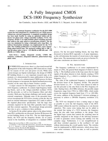
2054IEEE JOURNAL OF SOLID-STATE CIRCUITS, VOL. 33, NO. 12, DECEMBER 1998A Fully Integrated CMOSDCS-1800 Frequency SynthesizerJan Craninckx, Student Member, IEEE, and Michel S. J. Steyaert, Senior Member, IEEEAbstract—A prototype frequency synthesizer for the DCS-1800system has been integrated in a standard 0.4- m CMOS processwithout any external components. A completely monolithic designhas been made feasible by using an optimized hollow-coil inductor low-phase-noise voltage-controlled oscillator (VCO). Thefrequency divider is an eight-modulus phase-switching prescalerthat achieves the same speed as asynchronous dividers. The diearea was minimized by using a dual-path active loop filter. Anindirect linearization technique was implemented for the VCOgain. The resulting architecture is a fourth-order, type-2 chargepump phase-locked loop. The measured settling time is 300 s,and the phase noise is up to 0123 dBc/Hz at 600 kHz and 0138dBc/Hz at 3-MHz offset.Index Terms— Analog integrated circuits, CMOS RF,frequency synthesizer, integrated inductors, phase-locked loop,phase noise.Fig. 1. PLL frequency synthesizer.process. For the low-speed building blocks, the loop filterdiscussed in Section III-D especially is of great importance,as this will determine the transfer of circuit noise to the outputphase noise. The measurement results are given in Section IV,and some conclusions are drawn in Section V.I. INTRODUCTIONII. PLL ARCHITECTUREIN WIRELESS transceivers, there is a clear trend toward fullintegration of the radio-frequency (RF) front end on a singledie for reasons of low cost and power [1]–[4]. While mostcurrent designs use bipolar technologies, the design of CMOSRF building blocks is a very important research topic at themoment, as is demonstrated by many publications in that area[5]–[12]. The use of a submicrometer CMOS process for thesecircuits prepares to incorporate the digital baseband processingcircuitry on the same chip in future wireless systems.A major concern for full integration is the local oscillator(LO) frequency synthesizer. It contains high-frequency building blocks, such as the voltage-controlled oscillator (VCO)and the prescaler, as well as low-frequency filters and othercircuitry. Both pose big design challenges and mostly requireexternal components. Although some of the presented transceivers incorporate the VCO active circuitry on the die, they allneed an external inductance–capacitance (LC) tank to achievethe required phase-noise specification. And the large timeconstants required for the loop filter generally lead to largeand thus external capacitors. The prototype design presentedhere tries to give a solution to these problems.In Section II, the global options taken in the phase-lockedloop (PLL) architecture are discussed. Section III discusses theseveral building blocks of the PLL. The two high-frequencyblocks, the VCO and the frequency divider, are of coursecrucial in the feasibility of integration in a standard CMOSManuscript received May 6, 1998; revised July 6, 1998.J. Craninckx is with Alcatel Microelectronics, Zaventem B-1930 Belgium.M. S. J. Steyaert is with the Department Elektrotechniek, KatholiekeUniversiteit Leuven, Heverlee B-3001 Belgium.Publisher Item Identifier S 0018-9200(98)08877-5.The frequency synthesizer is of course implemented bymeans of a PLL, the general block diagram of which is shownin Fig. 1. The feedback action in the loop causes the two inputsignals of the phase detector to lock, thereby creating a VCO, which is a multiple of the referenceoutput frequency.frequencyThe value of the synthesized frequency is determined bythe division factor of the frequency divider. The prescaler71) have been chosen in order todivision factors (i.e., 64use this prescaler as the only block in the PLL frequency divider. Starting from a 26.6-MHz reference, the possible outputfrequencies range from 1702.4 to 1888.6 MHz, which neatlycovers the required frequency band from 1.71 to 1.88 GHz.Of course, addition of the fractional- division technique isnecessary to achieve a 200-kHz frequency resolution [13],[14].The VCO was designed to have a tuning range as largeas possible to cover the full frequency band of the DCS1800 system without the need for switching in or out discretecapacitors. This coarse extra tuning that can be added tothe normal fine tuning of a VCO increases the frequencyrange but also adds some problems to the design. First,the digital logic system that controls the switching must becarefully integrated in the design of the full-loop dynamicsin order to guarantee correct locking and stability over thecomplete range. Furthermore, it is not straightforward toadd these switched capacitors to the oscillator’s LC tankwithout deteriorating the overall quality factor. The switchesmust be implemented as MOS transistors, which always havesome series resistance in their on state, as well as parasitic0018–9200/98 10.00 1998 IEEE
CRANINCKX AND STEYAERT: FREQUENCY SYNTHESIZERjunction capacitance to the substrate from their source anddrain regions. So the circuit design as well as the layout willhave an important influence on the resulting quality factor.A drawback of this “single-step” VCO tuning is the fact thatthe VCO sensitivity must be very large, which will have itsconsequences in the various transfer functions of charge pumpand loop filter noise to the output. This will be investigated inSection III-D. Second, the fact that the junction capacitanceused for VCO tuning cannot always be biased far from theforward region for the lower frequency range will increasethe nonlinearities in the VCO. As a result, upconverted lownoise will have a larger contribution to thefrequencyVCO phase noise [15]. This is a problem that has not beensolved yet.2055(a)(b)Fig. 2. Planar inductor coil shape: (a) standard octagonal and (b) symmetrical.TABLE IOPTIMIZED COIL PARAMETERSIII. PLL BUILDING BLOCKSA. Voltage-Controlled OscillatorThe performance of planar inductors has improved recentlydue to efficient analysis of the parasitics with finite-elementsimulation techniques [11], [12]. These studies have resultedin some general guidelines for designing high-quality spiralinductors on silicon substrates.1) Limit the width of the metal conductors: This is due to amore important increase in the high-frequency resistancebecause of the skin effect.2) Use minimum spacing in between the conductors: Thiswill maximize the inductance value, and the fringingcapacitance is generally negligible.3) Do not fill the inductor up to the center: The innermosttracks contribute only a small amount of inductance, butdue to eddy currents generated by the magnetic field ofthe outer turns, their high-frequency resistance increasesenormously. It is best if they are simply omitted. Thisleads to the hollow coil shape.4) Limit the area occupied by the coil: This way, themagnetic field penetrates less deeply into the substrate,and the associated substrate losses will be smaller. Thisguideline is only valid for conductive substrates, as thesubstrate currents in lowly doped wafers are alreadysmall.As the process available for this design uses nonepi wafers,the substrate resistivity is high enough to indeed neglect thelast guideline. This generally leads to larger values of forthe optimal coil. This is not always an advantage, as largeinductance values lead to a smaller capacitance value andhence less tuning range, if an important part of the capacitanceis already accounted for by the coil and transistor parasitics.Using two coils in series to form a balanced inductor will resultin this constraint. The optimum VCO design must include onlyone coil in the inductor.Therefore, a new coil shape was developed, as shown inFig. 2. Instead of drawing a normal spiral track and then making the connection to the inner turn in a different metallizationlevel, the metal track now moves inside every half turn, untilthe center is reached, and then moves outside again everyhalf turn. Both the Metal1 and Metal2 routing levels are used,except for the cross sections, which use of course only onemetal level for each direction. The number of cross sections isequal for both shapes, so this new shape has no effect on thedc series resistance. This coil is completely symmetrical andcan thus be used as a differential floating inductor. Using thefinite-element optimization procedure described in [11], thecoil parameters given in Table I are obtained. In spite of thefact that only two metal layers are available, a quality factoras high as 8.6 is reached.The oscillator circuit schematic is shown in Fig. 3. Thenegative resistance is formed by the double cross connection of–and a PMOS–differential pairan NMOSin positive feedback. In a 3-V system, the supply current canbe used twice for amplification with this circuit. A drawback ofthis configuration is of course the larger parasitic capacitancesof the PMOS transistors with respect to an NMOS-onlyimplementation. This will result in a slightly smaller availabletuning range as the fixed part of the tank capacitance hasincreased. The use of slower PMOS transistors in this oscillatorconfiguration is no problem, as the gate–source capacitance issituated in parallel with the resonance tank. An advantage isthat there is no need for a connection to the common-modepoint of the inductor, which would be a problem for the newsymmetrical coil shape. The frequency tuning is done withthe standard available P /N-well junction capacitors. The biascurrent is set at 3.7 mA, and the transistors are biased atV.The measured free-running oscillation frequency is 1.99GHz, which is only 0.5% off of the predicted value of 1.98GHz. The resulting phase noise was measured with a spectrum
2056IEEE JOURNAL OF SOLID-STATE CIRCUITS, VOL. 33, NO. 12, DECEMBER 1998which is optimized to avoid glitches in the output. As willbe shown in the following paragraphs, two pumps must beimplemented, but the control signals are of course reused.The loop-filter design is a big challenge, as it determinesthe PLL settling time and the output phase-noise characteristicand is responsible for the biggest contribution to the chip areabecause of the integrated capacitors. This filter will determinewhether the DCS-1800 phase-noise specifications of 119dBc/Hz at 600 kHz offset and 136 dBc/Hz at 3-MHz offsetcan be met.The simplest configuration is a passive filter that uses twocapacitors and a resistor, as shown in Fig. 7. The resultingPLL is then a type-2, third order.The open loop gain equalsFig. 3. Planar-LC oscillator circuit schematic.analyzer to be 113 dBc/Hz at 200 kHz offset. Extrapolatingthis to 600 kHz results in 122.5 dBc/Hz. A 20% frequencyrange from 1.62 to 1.99 GHz can be covered [12].B. PrescalerWith the phase-switching prescaler architecture of Fig. 4,multimodulus prescalers can be realized that do not sufferfrom any speed degradation with respect to prescalers with afixed division ratio. This technique is based on the 90 phaserelationship between the outputs of the master and the slavesection of a master/slave divide-by-two toggle flip-flop [16].from a certainSwitching the phase-select output signalphase of these four differential quadrature outputs to the onethat lags the present signal inserts a 90 delay. This 90 atone-fourth of the input frequency is equivalent to a full periodof the input signal. The modulus control block is designed toinsert a number of the phase switches per output period,thereby increasing the normal division modulus from 64 to 64. The three bits of the control word Mode can set to anyvalue from zero to seven, so the resulting prescaler divisionmoduli range from 64 to 71.C. Phase DetectorThe phase-frequency detector schematic is shown in Fig. 5.It is the commonly employed circuit that inserts pulses on theup and down outputs of a certain minimum width, even whenthe phase difference is zero. This eliminates the dead-zoneproblem of the PLL, i.e., changes in the phase detector gainwhen the loop is in lock [17], [18].D. Loop FilterThe loop-filter charge-pump circuit is shown in Fig. 6. Boththe up and the down current can be either connected to theoutput or drained to a dummy reference voltage by the fourswitches. To minimize clock feedthrough, all switches areimplemented by an NMOS and a PMOS transistor, and everytransistor has its own control signal, the relative timing of(1)the VCO sensitivity,the charge-pump current,withthe frequency division modulus.andequals approximatelyThe cross-over frequency(2)a factor belowWe will place the loop gain zeroand the third polea factor aboveto guarantee enoughand are typically equal tophase margin. These factorsfour, which gives a phase margin of approximately 60 . Thesize of the passive elements can easily be calculated from theloop parameters(3)This configuration might seem a good solution at first sight,but it cannot be used here for two reasons. First, the outputvoltage, which is the VCO input control voltage, must varyover a wide range to use the full tuning range of the VCO.Due to the finite output impedance of the current sources, theup and down current cannot be matched over this full range.This will result in a small offset at the input of the phaseand frequency detector (PFD) and consequently cause spursin the output spectrum. Increasing the output impedance by,e.g., placing cascode transistors in the charge pump is also notpossible, as it will reduce drastically the output voltage rangeand hence also the frequency tuning range.The second reason this configuration cannot be used here isthe large contribution to the output phase noise of the thermalnoise in the charge pump and the loop filter resistors. For offset
CRANINCKX AND STEYAERT: FREQUENCY SYNTHESIZER2057Fig. 4. Eight-modulus phase-switching prescaler.Fig. 6. Charge-pump core circuit.Fig. 5. Phase-frequency detector without dead zone.frequencies larger thanwill have a dependency on the offset frequency ofThe following equations describe this behavior:., these can be approximated by(5)(4)is the overdrive voltage of the chargewhereis the fraction of time thesepump current sources andcurrent sources are active when the loop is in lock. For the, a very low loop bandwidth is neededcharge-pump noiseto reduce the phase noise to a value well below the DCS-1800, a very lowspecification. And for the filter resistor noiseis needed. Both equations hence lead to the usevalue forof extremely large capacitor values, which are not feasible forintegration.So a fourth pole must be inserted in the loop filter, as shownby makingin Fig. 8. The extra pole is placed on top of. We keep one degree of freedom in doing this, i.e.,a factor smaller than , we must increaseif we makeby the same amount. To keep the phase margin high enough,must be increased from four to six. Since the loop transferfunction now falls off at 60 dB/decade for frequencies beyond, the noise of the charge pump and the loop filter resistor(6)(7)(8)But also, this solution leads to a total capacitance that is toolarge to be integrated.Therefore, a special filter topology is employed that splitsup the loop filter in two paths, as was already done in[17]. The principle is explained in Fig. 9. The passive loopandactually forms a pole atfilter consisting of, and another pole atIt iszero frequency, a zero atthe capacitor creating the zero that has the largest size andhence poses difficulties in integration. In this new technique,the same filter characteristic is achieved by combining twocombination at thesignals, which does not need an actualfrequency of the zero.
2058IEEE JOURNAL OF SOLID-STATE CIRCUITS, VOL. 33, NO. 12, DECEMBER 1998(a)(a)(b)Fig. 7. (a) Third-order, type-2 charge-pump PLL passive filter. (b) Openloop gain Bode plot.The goal is to add two signals, which we will calland. The first signal is an integrated version of the input current.So it has a pole at zero frequency(b)Fig. 8. (a) Active loop filter for a fourth order, type-2 charge-pump PLL.(b) Open loop gain Bode plot.(9)The other signal path has a low-pass transfer function(10)These two signals are now added to form the complete outputsignal, but the second one is amplified by a factor . Thisresults inFig. 9. Dual-path loop filter principle.with(11)So a large time constant (or a low frequency) is realized forthe filter zero without the requirement for a large capacitor,profits from the multiplication by the factor . Theasimplementation for this configuration is shown in Fig. 10.The circuit has two input currents, one to be integrated toand one to be low-passed toThe impact on the chargepump design is minimal, as only the charge-pump core mustbe implemented twice. The control signals can be reused forboth parts. And multiplication of the second signal by a factoris also very easy to do, as this is done in the currentdomain by using a pump current that is a factor larger in thecharge-pump core driving the signal . Both input currentsare represented here with a negative sign, which means that theand theterminals must be interchangedposition of thein the phase-frequency detector. The adder that sums the twofromsignals is actually a subtracter the subtractsLast, a fourth pole is added by the combination ofand
CRANINCKX AND STEYAERT: FREQUENCY SYNTHESIZER2059(17)(18)(19)Fig. 10.Dual-path loop filter implementation.Moreover, in the configuration of Fig. 10, the dc operating. This isvoltage of both current inputs is positioned atobvious in the active integrator, but it is also true for the lowwhen the loop ispass path, as no current flows throughpath isin lock. So an active implementation for thenot necessary.The resulting PLL open loop gain is equal to(12)originates from the charge pump,andwherefrom the filter resistors,from the integrator amplifier, andfrom the adder.andrepresent the equivalentinput noise transconductance of the filter amplifier and adder,respectively. These equations illustrate the 60-dB per decaderolloff of the most important phase-noise contributions, i.e.,the charge pump and the resistorA behavioral linear model for the PLL implemented inSPICE, as shown in Fig. 11, was used to determine the loopandVoltages were used to representparametersthe phase of the input and output signals. The loop filtercan be implemented with ideal amplifiers or with real circuitschematics. Some biasing elements that are required to set allthe correct operating points are not indicated in the figure. Theappropriate noise sources can be introduced, and the resultingoutput phase noise is calculated with(20)The cross-over frequency is(13)can be neglected with respect to.provided thata factor below the loopWe will put the zerobandwidth. Considering the two high-frequency polesand, the best results for noise suppression outside the loopbandwidth versus phase margin are obtained if they coincide.So if the resistorWe will place them a factor aboveis made a factor smaller than,must be larger thanby the same amount. This gives the following equationsfor the passive element values:(14)The several contributions to the out-of-band output phasenoise can be approximated by(15)(16)Using this model, the loop parameters can be varied, andtheir effect on the PLL performance can be evaluated rapidly.andWe cannot change the relative position of the zerobecause the phase margin must be highthe two poles atandenough to maintain a stable system. So we putThe VCO gainequals at most400 MHz/V,is 64. So the remaining loopand the division modulusparameters that are incorporated into the optimization are thethe charge-pump currentthe filterloop bandwidthand the fourth pole parameterOur goal is tofactorachieve a low phase noise within two constraints. The firstconstraint is a low power consumption, which will be reflectedandThe secondin the restrictions on the values ofconstraint is the most important one and limits the occupiedchip area. We must limit the sum of the capacitor sizes ofandto a value realizable in an integrated circuit.The final optimized loop parameters are listed in Table II.A pump current of 1 A is used, and the loop bandwidthequals 45 kHz. This should be sufficiently large for the settlingtime. The total capacitance value is as large as 960 pF. Thiswill be responsible for a large chip area, but it is the onlyway to achieve the required low phase noise. Even with thesevalues, the spec is only achieved without any margin, i.e., anyother phase noise introduced in the circuit will cause the phasenoise to be higher than allowed in the DCS-1800 system. Thesituation is, however, much relaxed at lower VCO gains, whichappear rapidly at slightly higher output frequencies. So therequired specs will be achieved over most of the frequencyrange.Fig. 12 shows the simulated open-loop gain, which hasindeed a cross-over frequency of 45 kHz. The phase marginis 58 a value that is high enough to avoid excessive ringing
2060Fig. 11.IEEE JOURNAL OF SOLID-STATE CIRCUITS, VOL. 33, NO. 12, DECEMBER 1998Behavioral SPICE PLL model.TABLE IIFINAL PLL PARAMETERSfor the integrating current path andforthe low-pass path). In the middle graph, the phase noiserelated to the thermal noise in the two resistorsandis shown. Last, the bottom graph lists thephase noise originating from the active elements used in therepresents the noise from the integratorloop filter.is due to the adder. We can clearly seeamplifier andorin all graphs for highthe dependency onoffset frequencies. The values at 600 kHz were already listedin the above table, and they agree very well with the theoreticalformulas (15)–(19).E. Linearizationand slow settling. In the charge pump, an on-time fractionof 0.1 and aof 0.3 V has been assumed.Fig. 13 shows the several phase-noise contributions versusfrequency for the designed loop parameters. The first graphshows the phase noise originating in the two charge pumpsBecause the standard available P /N-well junction capacisitance has been used for the VCO tuning, its gainhighly nonlinear. As this changes the overall PLL loop gain,the feedback will become unstable if no countermeasures aretaken. The insertion of a linearization block in between theloop filter and the VCO is not feasible for noise reasons.Indeed, noise inserted at this point is not suppressed atoffset frequencies larger than the loop bandwidth. The powerconsumption needed to bring the linearization noise below therequired level is too high.Instead, it can be noted from (12) that the open loopgain is proportional to the product of the VCO gain andthe charge-pump current. In the presented design, this currentis adjusted to the proper value, dependent on the valueA six-step piece-wise linear fitting of the VCOoftuning characteristic is used in the linearization block ofthe PLL to switch on/off the required current sources in a
CRANINCKX AND STEYAERT: FREQUENCY SYNTHESIZERFig. 12.2061Simulated PLL open-loop gain.current mirror bank. The block diagram of the linearizationcircuitry is shown in Fig. 14.The VCO control voltage is compared with five referencevoltages. These reference levels are generated with the resistorand the transistorThe transistorstringtracks the absolute value of the NMOS threshold voltage,and hence also tracks the VCO tuning curve, whose absolute position is partly determined by the NMOS amplifyingtransistors in the oscillator schematic. The five switch-controlare used to add or remove current sources fromsignalsSchmitt triggers are inserted to providethe output currentsome hysteresis and avoid instabilities around the thresholdvoltages. The output current is fed to the charge pump to setandThis approach has thethe nominal current ofadvantage that almost no extra phase noise is introduced. Noisepresent in the linearization output is fed to the up as well asthe down current source in the charge pump. In lock, bothcurrent sources are active for a short duration of time (givenbut they both contain the same amount ofby the fractionlinearization noise, which cancels out since the two currentsare subtracted.IV. MEASUREMENT RESULTSAll the circuits described above have been implementedin a single IC, shown in Fig. 15. The hollow coil used inthe VCO can be clearly distinguished in the lower right-handcorner of the die. The prescaler is situated in the lower lefthand corner. The largest part of the IC is occupied by thethree filter capacitors. They are realized using the poly/polystructure available in this process with a nominal capacitancevalue of 1.5 fF/. The active filter amplifiers are placed inbetween these capacitors. The phase-frequency detector andthe charge pump are situated in the middle on the left-handside of the die, and the linearization circuitry occupies the1.9 m .upper left-hand corner. The total die size is 1.7The reference frequency is 26.6 MHz, and the power-supplyvoltage is 3 V for all circuits. The power consumption of thechip is 51 mW, which is divided over the several buildingblocks as follows: PFD one, charge pump one, loop filter 18,VCO 11, prescaler 18, and linearization 2 mW.An important aspect of the variation of the VCO gain withfrequency is of course the different noise-transfer functions andhence different output phase noise. This is even deterioratednoise in the VCO itself at low tuningby the increase involtages. Fig. 16 shows the output spectrum for two outputfrequencies, i.e., 1.71 and 1.88 GHz. The measurement wasperformed using a dedicated phase-noise measurement setupthat is based on the delay-line method. Outside the loop band45 kHz), we clearly see the dominant VCO noise.widthFor the 1.71-GHz signal, it consists mainly of upconverted
2062Fig. 13.Fig. 14.IEEE JOURNAL OF SOLID-STATE CIRCUITS, VOL. 33, NO. 12, DECEMBER 1998Simulated PLL output phase noise.Indirect linearization circuitry for the PLL.noise, which results in a magnitude of 115 dBc/Hz at600-kHz offset. Because of the smaller nonlinearities whenoperating at 1.88 GHz, the VCO spectrum is much cleanerand the PLL phase noise is correspondingly lower, downto 123 dBc/Hz at 600 kHz, which is sufficient accordingto the DCS-1800 specification. Further from the carrier, themeasured phase noise at 3-MHz offset is 134 dBc/Hz and138 dBc/Hz for the two output frequencies shown.Inside the loop bandwidth, it is not the charge-pump noisethat is dominant, as would be predicted by the simulationsperformed in Fig. 13. Unfortunately, missing data on thenoise of the transistors in the active filter circuitry caused us tonoise of the biasing circuitry for the amplifieroverlook theand adder in the active filter. Therefore, the in-band phasenoise is higher than expected but still remains below 75dBc/Hz. Closer to the carrier, the phase noise increases againdue to the reference-signal phase-noise feedthrough.The second important thing that has been measured is theFig. 17settling time after a change in the division factorcompares the simulated and measured waveforms of the VCOcontrol voltage when changing the division modulus from64 to 68 and back. Mixed-signal simulations predict a risetime of approximately 120 s and a settling to a 100-Hzaccuracy within 250 s. The measurement is not accurateenough to determine the actual settling time to a voltagewith V accuracy, but based on the simulations and the smalldifference in rise time, we can conclude that the PLL has asettling time smaller than 300 s.V. CONCLUSIONSIn this paper, we have described a working prototypefor a monolithic CMOS DCS-1800 frequency synthesizer.The integrated VCO uses an optimized hollow coil with a
CRANINCKX AND STEYAERT: FREQUENCY SYNTHESIZER2063Fig. 15.IC microphotograph.Fig. 16.Measured PLL output phase noise at two extreme output frequencies.quality factor of 8.6 to achieve the required phase noise withminimal power consumption. The phase-switching prescalerarchitecture allows the implementation of multimodulus dividers without a speed penalty with respect to fixed prescalers.Most design effort has been put in the loop filter and thelinearization. The dual-path loop filter circuit uses two signalpaths, one of which uses a scaled current, to create a smalltime constant without the need for very large capacitor values.
2064Fig. 17.IEEE JOURNAL OF SOLID-STATE CIRCUITS, VOL. 33, NO. 12, DECEMBER 1998Measured PLL settling.A behavioral model of the PLL was implemented in SPICEto optimize the loop parameters for low noise and low area.An indirect linearization technique was used for the VCO thatkeeps the product of the charge-pump current and the VCOgain constant over the complete frequency range, which isalso sufficient to create a constant open loop gain, and henceassures stability.1.9 mm die in aThe PLL was realized on a 1.7standard 0.4- m CMOS process. Of course, it uses no external components and functions without tuning, trimming, orpostprocessing steps. It consumes 51 mW from a single 3V power supply. The loop bandwidth is 45 kHz, and a totalcapacitance of almost 1 nF is integrated.The output phase noise complies with the DCS-1800 standard of 119 dBc/Hz at 600 kHz offset apart from twonoise.remaining problems, both of which are related tonoise of the VCO for theThe first one is the too-highlowest output frequencies, which is caused by the increasednonlinearities when the tuning junction capacitances are biasedin almost-forward conditions. The second problem can easilynoise in the biasingbe remedied because it originates fromcircuitry of the active filter amplifiers. The measured settlingtime for a 100-MHz frequency step is below 300 s, which isfast enough for the DCS-1800 standard.To conclude, we can state that although this design does notfulfill the DCS-1800 specification over the complete frequencyrange, it has demonstrated the feasibility of a full CMOS PLLwith no external components as the frequency synthesizer in amodern high-performant mobile communication system suchas DCS-1800. As a suggestion for further improvement of thePLL, we think that coarse tuning of the VCO with a binaryweighted bank of capaci
Title: A Fully Integrated CMOS DCS-1800 Frequency Synthesizer - Solid-State Cir cuits, IEEE Journal of Author