Transcription
LOGIC DESIGN LABORATORY MANUAL
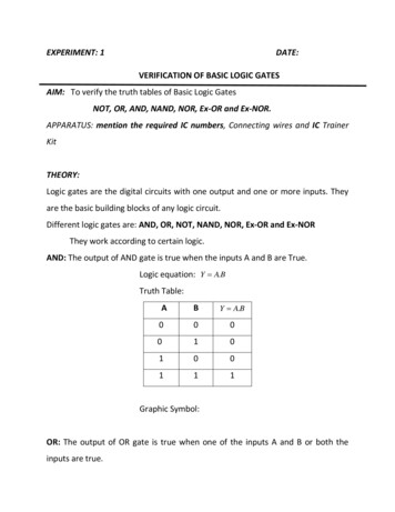
Logic Design Laboratory Manual1EXPERIMENT: 1LOGIC GATESAIM: To study and verify the truth table of logic gatesLEARNING OBJECTIVE: Identify various ICs and their specification.COMPONENTS REQUIRED: Logic gates (IC) trainer kit. Connecting patch chords. IC 7400, IC 7408, IC 7432, IC 7406, IC 7402, IC 7404, IC 7486THEORY:The basic logic gates are the building blocks of more complex logic circuits. These logicgates perform the basic Boolean functions, such as AND, OR, NAND, NOR, Inversion,Exclusive-OR, Exclusive-NOR. Fig. below shows the circuit symbol, Boolean function, andtruth. It is seen from the Fig that each gate has one or two binary inputs, A and B, and onebinary output, C. The small circle on the output of the circuit symbols designates the logiccomplement. The AND, OR, NAND, and NOR gates can be extended to have more than twoinputs. A gate can be extended to have multiple inputs if the binary operation it represents iscommutative and associative.These basic logic gates are implemented as small-scale integrated circuits (SSICs) or as partof more complex medium scale (MSI) or very large-scale (VLSI) integrated circuits. DigitalIC gates are classified not only by their logic operation, but also the specific logic-circuitfamily to which they belong. Each logic family has its own basic electronic circuit uponwhich more complex digital circuits and functions are developed. The following logicfamilies are the most frequently used.TTL Transistor-transistor logicECL Emitter-coupled logicMOS Metal-oxide semiconductorCMOS Complementary metal-oxide semiconductorTTL and ECL are based upon bipolar transistors. TTL has a well established popularityamong logic families. ECL is used only in systems requiring high-speed operation. MOS andCMOS, are based on field effect transistors. They are widely used in large scale integratedcircuits because of their high component density and relatively low power consumption.CMOS logic consumes far less power than MOS logic. There are various commercial
Logic Design Laboratory Manual2integrated circuit chips available. TTL ICs are usually distinguished by numerical designationas the 5400 and 7400 series.PROCEDURE:1. Check the components for their working.2. Insert the appropriate IC into the IC base.3. Make connections as shown in the circuit diagram.4. Provide the input data via the input switches and observe the output on output LEDs
Logic Design Laboratory Manual3VIVA QUESTIONS:1. Why NAND & NOR gates are called universal gates?2. Realize the EX – OR gates using minimum number of NAND gates.3. Give the truth table for EX-NOR and realize using NAND gates?4. What are the logic low and High levels of TTL IC’s and CMOS IC’s?5. Compare TTL logic family with CMOS family?6. Which logic family is fastest and which has low power dissipation?EXPERIMENT: 2REALIZATION OF A BOOLEAN FUNCTION.AIM: To simplify the given expression and to realize it using Basic gates andUniversal gatesLEARNING OBJECTIVE: To simplify the Boolean expression and to build the logic circuit. Given a Truth table to derive the Boolean expressions and build the logic circuit torealize it.COMPONENTS REQUIRED:IC 7400, IC 7408, IC 7432, IC 7406, IC 7402, Patch Cords & IC Trainer Kit.THEORY:Canonical Forms (Normal Forms): Any Boolean function can be written in disjunctivenormal form (sum of min-terms) or conjunctive normal form (product of max-terms).A Boolean function can be represented by a Karnaugh map in which each cell corresponds toa minterm. The cells are arranged in such a way that any two immediately adjacent cellscorrespond to two minterms of distance 1. There is more than one way to construct a mapwith this property.Karnaugh MapsFor a function of two variables, say, f(x, y),For a function of three variables, say, f(x, y, z)For a function of four variables: f(w, x, y, z)
Logic Design Laboratory Manual4Realization of Boolean expression:1)Y A B C D A BC D ABC D A B C D A B C D A B C D A B CDAB1111111After simplifying using K-Map method we getY A B C DTRUTH TABLERealization using Basic gatesRealization using NAND gatesRealization using NOR 10
Logic Design Laboratory Manual52) For the given Truth Table, realize a logical circuit using basic gates and NAND 01PROCEDURE:Check the components for their working.Insert the appropriate IC into the IC base.Make connections as shown in the circuit diagram.Provide the input data via the input switches and observe the output on output LEDsVerify the Truth TableRESULT: Simplified and verified the Boolean function using basic gates and universal gatesVIVA QUESTIONS:1) What are the different methods to obtain minimal expression?2) What is a Min term and Max term3) State the difference between SOP and POS.
Logic Design Laboratory Manual64) What is meant by canonical representation?5) What is K-map? Why is it used?6) What are universal gates?EXPERIMENT: 3ADDERS AND SUBTRACTORSAIM: To realizei) Half Adder and Full Adderii) Half Subtractor and Full Subtractor by using Basic gates and NAND gatesLEARNING OBJECTIVE: To realize the adder and subtractor circuits using basic gates and universal gates To realize full adder using two half adders To realize a full subtractor using two half subtractorsCOMPONENTS REQUIRED:IC 7400, IC 7408, IC 7486, IC 7432, Patch Cords & IC Trainer Kit.THEORY:Half-Adder: A combinational logic circuit that performs the addition of two data bits, A andB, is called a half-adder. Addition will result in two output bits; one of which is the sum bit,S, and the other is the carry bit, C. The Boolean functions describing the half-adder are:S A BC ABFull-Adder: The half-adder does not take the carry bit from its previous stage into account.This carry bit from its previous stage is called carry-in bit. A combinational logic circuit thatadds two data bits, A and B, and a carry-in bit, Cin , is called a full-adder. The Booleanfunctions describing the full-adder are:S (x y) CinC xy Cin (x y)Half Subtractor: Subtracting a single-bit binary value B from another A (i.e. A -B ) producesa difference bit D and a borrow out bit B-out. This operation is called half subtraction and thecircuit to realize it is called a half subtractor. The Boolean functions describing the halfSubtractor are:S A BC A’ BFull Subtractor: Subtracting two single-bit binary values, B, Cin from a single-bit value Aproduces a difference bit D and a borrow out Br bit. This is called full subtraction. TheBoolean functions describing the full-subtracter are:D (x y) CinBr A’B A’(Cin) B(Cin)
Logic Design Laboratory Manual7I.TO REALIZE HALF ADDERTRUTH TABLEINPUTS OUTPUTSABSC0000011010101101i) Basic GatesII.BOOLEAN EXPRESSIONS:S A BC A Bii) NAND GatesFULL ADDERTRUTH TABLEINPUTSBOOLEAN 0101011100111111i)BASIC GATESS A B CC A B B Cin A Cin
Logic Design Laboratory Manual8ii) NAND GATESIII.HALF SUBTRACTORTRUTH TABLEINPUTSABBOOLEAN EXPRESSIONS:OUTPUTSDBr0000011110101100D A BBr A B
Logic Design Laboratory Manual9i)BASIC GATESIV.ii) NAND GatesFULL SUBTRACTORTRUTH TABLEINPUTSBOOLEAN 10101001100011111i) BASIC GATESD A B CBr A B B Cin A Cin
Logic Design Laboratory Manual10ii) To Realize the Full subtractor using NAND Gates only PROCEDURE:Check the components for their working.Insert the appropriate IC into the IC base.Make connections as shown in the circuit diagram.Verify the Truth Table and observe the outputs.RESULT: The truth table of the above circuits is verified.VIVA QUESTIONS:1) What is a half adder?2) What is a full adder?3) What are the applications of adders?4) What is a half subtractor?5) What is a full subtractor?6) What are the applications of subtractors?7) Obtain the minimal expression for above circuits.8) Realize a full adder using two half adders9) Realize a full subtractors using two half subtractors
Logic Design Laboratory Manual11EXPERIMENT: 4PARALLEL ADDER AND SUBTRACTORAIM: To design and set up the following circuit using IC 7483.i)A 4-bit binary parallel adder.ii)A 4-bit binary parallel subtractor.LEARNING OBJECTIVE: To learn about IC 7483 and its internal structure. To realize a subtractor using adder IC 7483COMPONENTS REQUIRED:IC 7483, IC 7486, Patch Cords & IC Trainer Kit.THEORY:The Full adder can add single-digit binary numbers and carries. The largest sum that can beobtained using a full adder is 112. Parallel adders can add multiple-digit numbers. If fulladders are placed in parallel, we can add two- or four-digit numbers or any other size desired.Figure below uses STANDARD SYMBOLS to show a parallel adder capable of adding two,two-digit binary numbers The addend would be on A inputs, and the augend on the B inputs.For this explanation we will assume there is no input to C0 (carry from a previous circuit)To add 102 (addend) and 012 (augend), the addend inputs will be 1 on A2 and 0 on A1. Theaugend inputs will be 0 on B2 and 1 on B1. Working from right to left, as we do in normaladdition, let’s calculate the outputs of each full adder. With A1 at 0 and B1 at 1, the output ofadder1 will be a sum (S1) of 1 with no carry (C1). Since A2 is 1 and B2 is 0, we have a sum(S2) of 1 with no carry (C2) from adder1. To determine the sum, read the outputs (C2, S2, andS1) from left to right. In this case, C2 0, S2 1, and S1 1. The sum, then, of 102 and 012
Logic Design Laboratory Manual12is 0112. To add four bits we require four full adders arranged in parallel. IC 7483 is a 4- bitparallel adder whose pin diagram is shown.MSBINPUTSOUTPUTCoutA3B3S3A2B2S2IC 7483 pin diagrami)4-Bit Binary AdderAn Example: 7 2 11 (1001) 7 is realized at A3 A2 A1 A0 01112 is realized at B3 B2 B1 B0 0010Sum 1001ADDER CIRCUIT:A1B1S1LSBCinA0B0S0
Logic Design Laboratory Manual13PROCEDURE: Check all the components for their working. Insert the appropriate IC into the IC base. Make connections as shown in the circuit diagram. Apply augend and addend bits on A and B and cin 0. Verify the results and observe the outputs.ii)4-BIT BINARY SUBTRACTOR.Subtraction is carried out by adding 2’s complement of the subtrahend.Example: 8 – 3 5 (0101) 8 is realized at A3 A2 A1 A03 is realized at B3 B2 B1 B0 through X-OR gatesOutput of X-OR gate is 1’s complement of 32’s Complement can be obtained by adding CinThereforeCin 1A3 A2 A1 A0 1 0 0 0B3 B2 B1 B0 1 1 0 0S3 S2 S1 S0 0 1 0 1Cout 1 (Ignored) 1000 0011 1100 1
Logic Design Laboratory Manual14PROCEDURE: Check all the components for their working. Insert the appropriate IC into the IC base. Make connections as shown in the circuit diagram. Apply Minuend and subtrahend bits on A and B and cin 1. Verify the results and observe the outputs.RESULTS: Verified the working of IC 7483 as adder and subtractor.EXPERIMENT: 5BCD TO EXCESS- 3 CODE CONVERTERS.AIM: To design and realize the following using IC 7483.I)BCD to Excess- 3 CodeII)Excess-3 to BCD Code.LEARNING OBJECTIVE: To learn to realize BCD to Excess-3 code using adder IC 7483 To learn to realize Excess-3 to BCD Code using adder IC 7483COMPONENTS REQUIRED:IC 7483, IC 7486, Patch Cords & IC Trainer Kit.THEORY:
Logic Design Laboratory Manual15Code converter is a combinational circuit that translates the input code word into a newcorresponding word. The excess-3 code digit is obtained by adding three to the correspondingBCD digit. To Construct a BCD-to-excess-3-code converter with a 4-bit adder feed BCDcode to the 4-bit adder as the first operand and then feed constant 3 as the second operand.The output is the corresponding excess-3 code.To make it work as a excess-3 to BCD converter, we feed excess-3 code as the first operandand then feed 2's complement of 3 as the second operand. The output is the BCD code.Circuit DiagramTRUTH TABLE:i)BCD - EXCESS-3 CODEBCDii)EX-30 0 0 000110 0 0 101000 0 1 001010 0 1 101100 1 0 001110 1 0 110000 1 1 01001EXCESS-3 TO BCD CODE
Logic Design Laboratory Manual160 1 1 110101 0 0 010111 0 0 E: Check all the components for their working. Insert the appropriate IC into the IC base. Make connections as shown in the circuit diagram. Apply BCD code as first operand(A) and binary 3 as second operand(B) and cin 0 forRealizing BCD-to-Excess-3-code: Apply Excess-3-code code as first operand(A) and binary 3 as second operand(B) andCin 1 for realizing Excess-3-code to BCD. Verify the Truth Table and observe the outputs.RESULT: Realized BCD code to Excess-3 code conversion and vice versa using 7483 ICVIVA QUESTIONS:1) What is the internal structure of 7483 IC?2) What do you mean by code conversion?3) What are the applications of code conversion?4) How do you realize a subtractor using full adder?5) What is a ripple Adder? What are its disadvantages?EXPERIMENT: 6BINARY TO GRAY CODE CONVERTERAIM: To realize Binary to Gray code converter and vice versa.
Logic Design Laboratory Manual17LEARNING OBJECTIVE: To learn the importance of non-weighted code To learn to generate gray codeCOMPONENTS REQUIRED:IC 7400, IC 7486, and IC 7408, Patch Cords & IC Trainer KitI) BINARY TO GRAY CONVERSIONBinaryGrayB3 B2 B1 B0 G3 G2 G1 G000110010000G3 101100110100110010000111100001111G2 B3 B2G1 B1 B2G0 B1 B0BOOLEAN EXPRESSIONS:G3 B3G2 B3 B2G1 B1 B2; G0 B1 B0
Logic Design Laboratory Manual18BINARY TO GRAY CODE USING EX-OR GATESREALIZATION USING NAND GATES:II) GRAY TO BINARY CONVERSION0011001100110011B3 G3
Logic Design Laboratory Manual190101010101010101GrayBinaryB2 G3 G2G3 G2 G1 G0 B3 B2 B1 101001011010B1 G3 G2 G1B0 G3 G2 G1 G0BOOLEAN EXPRESSIONS:B3 G3B2 G3 G2B1 G3 G2 G1B0 G3 G2 G1 G0GRAY TO BINARY CODE CONVERSION USING EX-OR GATES
Logic Design Laboratory Manual20REALIZATION USING NAND GATES:PROCEDURE: Check all the components for their working. Insert the appropriate IC into the IC base. Make connections as shown in the circuit diagram. Verify the Truth Table and observe the outputs.RESULT: Binary to gray code conversion and vice versa is realized using EX-OR gates andNAND gates.VIVA QUESTIONS:1) What are code converters?2) What is the necessity of code conversions?3) What is gray code?4) Realize the Boolean expressions fora) Binary to gray code conversionb) Gray to binary code conversion
Logic Design Laboratory Manual21EXPERIMENT: 7MULTIPLEXER AND DEMULTIPLEXERAIM: To design and set up the following circuit1)To design and set up a 4:1 Multiplexer (MUX) using only NAND gates.2)To design and set up a 1:4 Demultiplexer(DE-MUX) using only NAND gates.3)To verify the various functions of IC 74153(MUX) and IC 74139(DEMUX).4)To set up a Half/Full Adder and Half/Full Subtractor using IC 74153.LEARNING OBJECTIVE: To learn about various applications of multiplexer and de-multiplexer To learn and understand the working of IC 74153 and IC 74139 To learn to realize any function using MultiplexerTHEORY:Multiplexers are very useful components in digital systems. They transfer a large number ofinformation units over a smaller number of channels, (usually one channel) under the controlof selection signals. Multiplexer means many to one. A multiplexer is a circuit with manyinputs but only one output. By using control signals (select lines) we can select any input tothe output. Multiplexer is also called as data selector because the output bit depends on theinput data bit that is selected. The general multiplexer circuit has 2n input signals, ncontrol/select signals and 1 output signal.De-multiplexers perform the opposite function of multiplexers. They transfer a small numberof information units (usually one unit) over a larger number of channels under the control ofselection signals. The general de-multiplexer circuit has 1 input signal, n control/selectsignals and 2n output signals. De-multiplexer circuit can also be realized using a decodercircuit with enable.COMPONENTS REQUIRED:IC 7400, IC 7410, IC 7420, IC 7404, IC 74153, IC 74139, Patch Cords & IC Trainer Kit.i) 4:1 MULTIPLEXERInputs4:1MUXYE’SelectinputsOutput Y E’S1’S0’I0 E’S1’S0I1 E’S1S0’I2 E’S1S0I3
Logic Design Laboratory Manual22REALIZATION USING NAND GATESTRUTH TABLEOutputsSelectInputsEnableInputS1 X1100XX0X0100XX1X1110XXX00110XXX11VERIFY IC 74153 MUX (DUAL 4:1 MULTIPLEXER)Inputs
Logic Design Laboratory Manual23ii) DE-MUX USING NAND GATESEnable Data SelectInputs Input InputsOutputsEDS1 S0 Y3 Y2 Y1 TION OF IC 74139 (DEMUX)TRUTH 101Y111011Y010111
Logic Design Laboratory Manual24HALF ADDER USING MUX:DESIGN:SUMI0I10123AA’TRUTH TABLECARRYI0 ULL ADDER USING TRUTH 0100110010111I115AI326AI3371
Logic Design Laboratory Manual25FULL ADDER CIRCUITHALF SUBTRACTOR USING I101230A’TRUTH TABLEInputsOutputsA00B01D01Br0110101100
Logic Design Laboratory Manual26FULL SUBTRACTOR USING ROWI0I101450A’I226A’I3371TRUTH 11010110010001PROCEDURE: Check all the components for their working. Insert the appropriate IC into the IC base. Make connections as shown in the circuit diagram. Verify the Truth Table and observe the outputs.RESULT: Adder and subtractor circuits are realized using multiplexer IC 74153.VIVA QUESTIONS:1) What is a multiplexer?2) What is a de-multiplexer?3) What are the applications of multiplexer and de-multiplexer?4) Derive the Boolean expression for multiplexer and de-multiplexer.5) How do you realize a given function using multiplexer6) What is the difference between multiplexer & demultiplexer?7) In 2n to 1 multiplexer how many selection lines are there?8) How to get higher order multiplexers?9) Implement an 8:1 mux using 4:1 muxes?
Logic Design Laboratory Manual27EXPERIMENT: 8COMPARATORSAIM: To realize One & Two Bit Comparator and study of 7485 magnitude comparator.LEARNING OBJECTIVE: To learn about various applications of comparator To learn and understand the working of IC 7485 magnitude comparator To learn to realize 8-bit comparator using 4-bit comparatorTHEORY:Magnitude Comparator is a logical circuit, which compares two signals A and B andgenerates three logical outputs, whether A B, A B, or A B. IC 7485 is a highspeed 4-bit Magnitude comparator , which compares two 4-bit words . The A B Inputmust be held high for proper compare operation.COMPONENTS REQUIRED:IC 7400, IC 7410, IC 7420, IC 7432, IC 7486, IC 7402, IC 7408, IC 7404, IC 7485, PatchCords & IC Trainer Kit.1) 1- BIT COMPARATORTRUTH TABLEA B A BA B A BINPUTSAB00011011A B A B AB2)2- BIT COMPARATOR(A B) A1 B 1 A0 B 1 B 0 B 0 A1A0(A B) (A0 B0) (A1 B1) (A B) B1 A1 B0 A1 A 0 A 0 B1B 0OUTPUTSA B A B A B010001100010
Logic Design Laboratory Manual282-bit comparator circuit diagramTRUTH 011001100110011B00101010101010101A B0000100011001110OUTPUTSA B1000010000100001A B0111001100010000
Logic Design Laboratory Manual293)TO COMPARE THE GIVEN DATA USING 7485 001A BA BA BPROCEDURE: Check all the components for their working. Insert the appropriate IC into the IC base. Make connections as shown in the circuit diagram. Verify the Truth Table and observe the outputs.RESULT: One bit, two bit and four bit comparators are verified using basic gates andmagnitude comparator IC7485VIVA QUESTIONS:1)2)3)4)5)6)What is a comparator?What are the applications of comparator?Derive the Boolean expressions of one bit comparator and two bit comparators.How do you realize a higher magnitude comparator using lower bit comparatorDesign a 2 bit comparator using a single Logic gates?Design an 8 bit comparator using a two numbers of IC 7485?
Logic Design Laboratory Manual30EXPERIMENT: 9DECODERSAIM: To realize a decoder circuit using basic gates and to verify IC 74LS139LEARNING OBJECTIVE: To learn about working principle of decoder To learn and understand the working of IC 74LS139 To realize using basic gates as well as universal gatesCOMPONENTS REQUIRED:IC74LS139, IC 7400, IC 7408, IC 7432, IC 7404, IC 7410, Patch chords, & IC Trainer KitTHEORY:A decoder is a combinational circuit that connects the binary information from ‘n’ input linesto a maximum of 2n unique output lines. Decoder is also called a min-term generator/maxterm generator. A min-term generator is constructed using AND and NOT gates. Theappropriate output is indicated by logic 1 (positive logic). Max-term generator is constructedusing NAND gates. The appropriate output is indicated by logic 0 (Negative logic).The IC 74139 accepts two binary inputs and when enable provides 4 individual active lowoutputs. The device has 2 enable inputs (Two active low).CIRCUIT DIAGRAM:2:4 DECODER (MIN TERM GENERATOR):TRUTH TABLE:INPUTAB00011011OUTPUTY0 Y110010000Y20010Y30001BOOLAEN EXPRESSIONS:Y 0 ABY 1 ABY 2 ABY 3 AB
Logic Design Laboratory Manual31CIRCUIT DIAGRAM:2:4 DECODER (MAX TERM GENERATOR):TRUTH TABLE:INPUTAB00011011OUTPUTY0 Y101101111CIRCUIT DIAGRAM:Y21101Y31110
Logic Design Laboratory Manual32STUDY OF IC 74LS139:
Logic Design Laboratory Manual33PROCEDURE:1. Make the connections as per the circuit diagram.2. Change the values of G1, G2A, G2B, A, B, and C, using switches.3. Observe status of Y0, to Y7 on LED’s.4. Verify the truth table.RESULT: Verified the Operation of 3 to 8 DecoderVIVA QUESTIONS:1. What are the applications of decoder?2. What is the difference between decoder & encoder?3. For n- 2n decoder how many i/p lines & how many o/p lines?4. What are the different codes & their applications?5. What are code converters?6. Using 3:8 decoder and associated logic, implement a full adder?7. Implement a full subtractor using IC 74138?8. What is the difference between decoder and de-mux?
Logic Design Laboratory Manual34EXPERIMENT: 10BCD TO 7-SEGMENT DECODER/DRIVERAIM: To set up and test a 7-segment static display system to display numbers 0 to 9.LEARNING OBJECTIVE: To learn about various applications of decoder To learn and understand the working of IC 7447 To learn about types of seven-segment displayCOMPONENTS REQUIRED:IC7447, 7-Segment display (common anode), Patch chords, resistor (1KΩ) & IC Trainer KitTHEORY:The Light Emitting Diode (LED) finds its place in many applications in these modernelectronic fields. One of them is the Seven Segment Display. Seven-segment displayscontains the arrangement of the LEDs in “Eight” (8) passion, and a Dot (.) with a commonelectrode, lead (Anode or Cathode). The purpose of arranging it in that passion is that we canmake any number out of that by switching ON and OFF the particular LED's. Here is theblock diagram of the Seven Segment LED arrangement.The Light Emitting Diode (LED), finds its place in many applications in this modernelectronic fields. One of them is the Seven Segment Display. Seven-segment displayscontains the arrangement of the LEDs in “Eight” (8) passion, and a Dot (.) with a commonelectrode, lead (Anode or Cathode). The purpose of arranging it in that passion is that we canmake any number out of that by switching ON and OFF the particular LED's. Here is theblock diagram of the Seven Segment LED arrangement.LED’s are basically of two typesCommon Cathode (CC) -All the 8 anode legs uses only one cathode, which is common.Common Anode (CA)-The common leg for all the cathode is of Anode type.A decoder is a combinational circuit that connects the binary information from ‘n’ input linesto a maximum of 2n unique output lines. The IC7447 is a BCD to 7-segment patternconverter. The IC7447 takes the Binary Coded Decimal (BCD) as the input and outputs therelevant 7 segment code.
Logic Design Laboratory Manual35CIRCUIT DIAGRAM:TRUTH TABLE:BCD InputsD0000000011C0000111100B0011001100Output Logic Levels from IC 7447 to 0000d0100100101e0101110101PROCEDURE: Check all the components for their working. Insert the appropriate IC into the IC base. Make connections as shown in the circuit diagram. Verify the Truth Table and observe the outputs.VIVA QUESTIONS:1. What are the different types of LEDs?2. Draw the internal circuit diagram of an LED.3. What are the applications of 3456789
Logic Design Laboratory Manual36EXPERIMENT: 11ENCODERSAIM:1. To set up a circuit of Decimal-to-BCD Encoder using IC 74147.2. To design and set up a circuit of Hexadecimal-to-Binary Encoder using IC3. 74148 Encoders and IC 74157 MultiplexerLEARNING OBJECTIVE: To learn about various applications of Encoders To learn and understand the working of IC 74147 , IC 74148 & IC 74157 To learn to do code conversion using encodersCOMPONENTS REQUIRED:IC 74147, IC 74148, IC 74157, Patch chords & IC Trainer KitTHEORY:An encoder performs a function that is the opposite of decoder. It receives one or moresignals in an encoded format and output a code that can be processed by another logic circuit.One of the advantages of encoding data, or more often data addresses in computers, is that itreduces the number of required bits to represent data or addresses. For example, if a memoryhas 16 different locations, in order to access these 16 different locations, 16 lines (bits) arerequired if the addressing signals are in 1 out of n format. However, if we code the 16different addressesinto a binary format, then only 4 lines (bits) are required. Such a reduction improves thespeed of information processing in digital systems.CIRCUIT DIAGRAM:1)DECIMAL-TO BCD ENCODER USING IC 74147.TRUTH TABLEINPUTSOUTPUTSI1I2I3I4I5I6I7 I8 I9 A3 A2 A1 A01111111100110X X X X X X X010111X X X X X X0111000X X X X X01111001X X X X011111010X X X0111111011X 1
Logic Design Laboratory Manual372)OCTAL TO BINARY ENCODER USING IC 74148.TRUTH TABLEInputsE1 I03)I1I2I3OutputsI4I5I6I7 A2 A1 A0 GS E01X X X X X X X X111110111111100X X X X X X X0000010X X X X X X01001010X X X X X011010010X X X X0111011010X X X01111100010X AL TO BINARY ENCODER1111
Logic Design Laboratory Manual38TRUTH SI7 I8 I90 1 11 1 11 1 11 1 11 1 11 1 11 1 11 1 11 1 11 1 11 1 11 1 11 1 11 1 11 1 01 0 11 1 10 0 0I10 1110111110PROCEDURE: Check all the components for their working. Insert the appropriate IC into the IC base. Make connections as shown in the circuit diagram. Verify the Truth Table and observe the outputs.VIVA QUESTIONS:1. What is a priority encoder?2. What is the role of an encoder in communication?3. What is the advantage of using an encoder?4. What are the uses of validating I15111111110111111110Y3111111110000000010OUTPUTSY2 Y1 111000
Logic Design Laboratory Manual39EXPERIMENT: 12FLIP FLOPSAIM: Truth Table verification ofRS Flip Flop1)2)T type Flip Flop.D type Flip Flop.3)4)JK Flip Flop.5)JK Master Slave Flip Flop.LEARNING OBJECTIVE: To learn about various Flip-Flops To learn and understand the working of Master slave FF To learn about applications of FFs Conversion of one type of Flip flop to anotherCOMPONENTS REQUIRED:IC 7408, IC 7404, IC 7402, IC 7400, Patch Cords & IC Trainer Kit.THEORY:Logic circuits that incorporate memory cells are called sequential logic circuits; their outputdepends not only upon the present value of the input but also upon the previous values.Sequential logic circuits often require a timing generator (a clock) for their operation.The latch (flip-flop) is a basic bi-stable memory element widely used in sequential logiccircuits. Usually there are two outputs, Q and its complementary value.Some of the most widely used latches are listed below.SR LATCH:An S-R latch consists of two cross-coupled NOR gates. An S-R flip-flop can also be designusing cross-coupled NAND gates as shown. The truth tables of the circuits are shown below.A clocked S-R flip-flop has an additional clock input so that the S and R inputs areactive only when the clock is high. When the clock goes low, the state of flip-flop is latchedand cannot change until the clock goes high again. Therefore, the clocked S-R flip-flopis also called “enabled” S-R flip-flop.A D latch combines the S and R inputs of an S-R latch into one input by adding aninverter. When the clock is high, the output follows the D input, and when the clockgoes low, the state is latched.A S-R flip-flop can be converted to T-flip flop by connecting S input to Qb and R to Q.1)S-R LATCH:(A) LOGIC DIAGRAM(B) SYMBOL
Logic Design Laboratory Manual40TRUTH TABLESRQ Q b 00Q011001Qb10110*0*S R LATCH:TRUTH TABLES00112)R0101Q 1*10QQ b 1*01QbSR FLIP FLOP:CIRCUIT DIAGRAM:(A) LOGIC DIAGRAMS(B) SYMBOLTRUT
Logic Design Laboratory Manual 11 _ EXPERIMENT: 4 PARALLEL ADDER AND SUBTRACTOR AIM: To design and set up the following circuit using IC 7483. i) A 4-bit binary parallel adder. ii) A 4-bit binary parallel subtractor. LEARNING OBJECTIVE: To learn about IC 7483 and its intern