Transcription
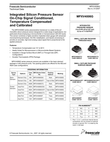
Freescale SemiconductorTechnical DataMPXV4006GRev 6, 01/2007Integrated Silicon Pressure SensorOn-Chip Signal Conditioned,Temperature Compensatedand CalibratedMPXV4006GINTEGRATEDPRESSURE SENSOR0 to 6 kPa (0 to 0.87 psi)0.2 to 4.7 V OUTPUTThe MPXV4006G series piezoresistive transducer is a state-of-the-artmonolithic silicon pressure sensor designed for a wide range of applications, butparticularly those employing a microcontroller or microprocessor with A/D inputs.This sensor combines a highly sensitive implanted strain gauge with advancedmicromachining techniques, thin-film metallization, and bipolar processing toprovide an accurate, high level analog output signal that is proportional to theapplied pressure.SMALL OUTLINE PACKAGETHROUGH-HOLEFeatures Temperature Compensated over 10 to 60 CIdeally Suited for Microprocessor or Microcontroller-Based SystemsAvailable in Gauge Surface Mount (SMT) or Through-hole (DIP)ConfigurationsDurable Thermoplastic (PPS) PackageJMPXV4006G7UCASE 482B-03MPXV4006G series pressure sensors are available in the basic elementpackage or with pressure ports. Two packing options are offered for the 482 and482A case configurations.MPXV4006GC7UCASE 482C-03SMALL OUTLINE PACKAGESURFACE MOUNTORDERING onsCase MPX Series OrderNo.No.Element Only482MPXV4006G6UElement 006GTape & Reel MPXV4006GElement Only482B MPXV4006G7URailsMPXV4006GAxial Port482A MPXV4006GC6URailsMPXV4006GAxial Port482A MPXV4006GC6T1 Tape & Reel MPXV4006GAxial Port482C MPXV4006GC7URailsMPXV4006GSide Port1369 MPXV4006GPTraysMPXV4006GDual Port1351 MPXV4006DPTraysMPXV4006GMPXV4006G6U/6T1 MPXV4006GC6U/C6T1CASE 482-01CASE 482A-01MPXV4006DPCASE 1351-01MPXV4006GPCASE 1369-01PIN NUMBERS(1)1N/C5N/C2VS6N/C3Gnd7N/C4Vout8N/C1. Pins 1, 5, 6, 7, and 8 are internal deviceconnections. Do not connect to externalcircuitry or ground. Pin 1 is noted by thenotch i n the lead. Freescale Semiconductor, Inc., 2007. All rights reserved.
VSGain Stage #2andGroundReferenceShift CircuitryThin FilmTemperatureCompensationandGain Stage #1SensingElementGNDVoutPins 1, 5, 6, 7, and 8 are NO CONNECTSfor small outline package deviceFigure 1. Fully Integrated Pressure Sensor SchematicTable 1. Maximum Ratings(1)ParametricsSymbolValueUnitsMaximum Pressure (P1 P2)Pmax24kPaStorage TemperatureTstg-30 to 100 COperating TemperatureTA-10 to 60 C1. Exposure beyond the specified limits may cause permanent damage or degradation to the device.Table 2. Operating essure RangePOP0—6.0kPaSupply Voltage(1)VS4.755.05.25VdcSupply CurrentIS——10mAdcFull Scale Output(2)(RF 51kΩ)VFSS—4.6—VOffset(3)(5)(RF �— 5.0%VFSSSensitivityAccuracy(4)(5)(10 to 60 C)1. Device is ratiometric within this specified excitation range.2. Full Scale Span (VFSS) is defined as the algebraic difference between the output voltage at full rated pressure and the output voltage at theminimum rated pressure.3. Offset (Voff) is defined as the output voltage at the minimum rated pressure.4. Accuracy (error budget) consists of the following: Linearity:Output deviation from a straight line relationship with pressure over the specified pressure range. Temperature Hysteresis: Output deviation at any temperature within the operating temperature range, after the temperature is cycled toand from the minimum or maximum operating temperature points, with zero differential pressure applied. Pressure Hysteresis:Output deviation at any pressure within the specified range, when this pressure is cycled to and from minimumor maximum rated pressure, at 25 C. Offset Stability:Output deviation, after 1000 temperature cycles, -30 to 100 C, and 1.5 million pressure cycles, withminimum rated pressure applied. TcSpan:Output deviation over the temperature range of 10 to 60 C, relative to 25 C. TcOffset:Output deviation with minimum pressure applied, over the temperature range of 10 to 60 C, relative to 25 C.5. Auto Zero at Factory Installation: Due to the sensitivity of the MPXV4006G, external mechanical stresses and mounting position can affectthe zero pressure output reading. To obtain the 5% FSS accuracy, the device output must be “autozeroed'' after installation. Autozeroing isdefined as storing the zero pressure output reading and subtracting this from the device's output during normal operations.MPXV4006G2SensorsFreescale Semiconductor
ON-CHIP TEMPERATURE COMPENSATION, CALIBRATION, AND SIGNAL CONDITIONINGThe performance over temperature is achieved byintegrating the shear-stress strain gauge, temperaturecompensation, calibration and signal conditioning circuitryonto a single monolithic chip.Figure 2 illustrates the gauge configuration in the basicchip carrier (Case 482). A fluorosilicone gel isolates the diesurface and wire bonds from the environment, while allowingthe pressure signal to be transmitted to the silicon diaphragm.The MPXV4006G series sensor operating characteristicsare based on use of dry air as pressure media. Media, otherthan dry air, may have adverse effects on sensorperformance and long-term reliability. Internal reliability andqualification test for dry air, and other media, are availableFluorosiliconeGel Die Coatfrom the factory. Contact the factory for information regardingmedia tolerance in your application.Figure 3 shows the recommended decoupling circuit forinterfacing the output of the integrated sensor to the A/D inputof a microprocessor or microcontroller. Proper decoupling ofthe power supply is recommended.Figure 4 shows the sensor output signal relative topressure input. Typical, minimum and maximum outputcurves are shown for operation over a temperature range of10 C to 60 C using the decoupling circuit shown in Figure 3.The output will saturate outside of the specified pressurerange.StainlessSteel CapDie 5 me1.0 µF0.01 µFGND470 pFP2Die BondDifferential SensingElementFigure 3. Recommended Power Supply Decouplingand Output Filtering Recommendations(For additional output filtering, please refer toApplication Note AN1646.)Figure 2. Cross Sectional Diagram SOP(Not to Scale)5Output (V)Transfer Function:4.5 Vout VS*[(0.1533*P) 0.045] 5% VFSS4 VS 5.0 V 0.25 VdcTEMP 10 to 60 C3.53Typical2.52Max1.5Min10.50036Differential Pressure (kPa)See Note 5 in Operating CharacteristicsFigure 4. Output versus Pressure DifferentialMPXV4006GSensorsFreescale Semiconductor3
PRESSURE (P1)/VACUUM (P2) SIDE IDENTIFICATION TABLEFreescale designates the two sides of the pressure sensoras the Pressure (P1) side and the Vacuum (P2) side. ThePressure (P1) side is the side containing silicone gel whichisolates the die from the environment. The pressure sensor isdesigned to operate with positive differential pressureapplied, P1 P2.The Pressure (P1) side may be identified by using thetable below:Table 3. Pressure (P1)/Vacuum (P2) Side Identification TablePart NumberCase TypeMPXV4006G6U/T1Pressure (P1) Side Identifier482Stainless Steel CapMPXV4006GC6U/T1482ASide with Port AttachedMPXV4006G7U482BStainless Steel CapMPXV4006GC7U482CSide with Port AttachedMPXV4006GP1369Side with Port AttachedMPXV4006DP1351Side with Part MarkingMINIMUM RECOMMENDED FOOTPRINT FOR SURFACE MOUNTED APPLICATIONSSurface mount board layout is a critical portion of the totaldesign. The footprint for the surface mount packages must bethe correct size to ensure proper solder connection interfacebetween the board and the package. With the correctfootprint, the packages will self align when subjected to asolder reflow process. It is always recommended to designboards with a solder mask layer to avoid bridging andshorting between solder pads.0.100 TYP2.540.66016.760.060 TYP 8X1.520.3007.620.100 TYP 8X2.54inchmmFigure 5. SOP Footprint (Case 482)MPXV4006G4SensorsFreescale Semiconductor
PACKAGE DIMENSIONS-A-D 8 PL0.25 (0.010)45MT BSASNOTES:1. DIMENSIONING AND TOLERANCING PER ANSIY14.5M, 1982.2. CONTROLLING DIMENSION: INCH.3. DIMENSION A AND B DO NOT INCLUDE MOLDPROTRUSION.4. MAXIMUM MOLD PROTRUSION 0.15 (0.006).5. ALL VERTICAL SURFACES 5 TYPICAL DRAFT.-BG81SNHCJ-TSEATINGPLANEPIN 1 IDENTIFIERKMDIMABCDGHJKMNSINCHESMINMAX0.415 0.4250.415 0.4250.212 0.2300.038 0.0420.100 BSC0.002 0.0100.009 0.0110.061 0.0710 7 0.405 0.4150.709 0.961.072.54 BSC0.050.250.230.281.551.800 7 10.2910.5418.0118.41CASE 482-01ISSUE OSMALL OUTLINE PACKAGESURFACE MOUNT-A-D40.25 (0.010)5N8 PLMT BSASNOTES:1. DIMENSIONING AND TOLERANCING PER ANSIY14.5M, 1982.2. CONTROLLING DIMENSION: INCH.3. DIMENSION A AND B DO NOT INCLUDE MOLDPROTRUSION.4. MAXIMUM MOLD PROTRUSION 0.15 (0.006).5. ALL VERTICAL SURFACES 5 TYPICAL DRAFT.-BG81SWVCHJ-TKMPIN 1 IDENTIFIERDIMABCDGHJKMNSVWINCHESMINMAX0.415 0.4250.415 0.4250.500 0.5200.038 0.0420.100 BSC0.002 0.0100.009 0.0110.061 0.0710 7 0.444 0.4480.709 0.7250.245 0.2550.115 210.961.072.54 BSC0.050.250.230.281.551.800 7 SE 482A-01ISSUE ASMALL OUTLINE PACKAGESURFACE MOUNTMPXV4006GSensorsFreescale Semiconductor5
PACKAGE DIMENSIONS-ANOTES:1. DIMENSIONING AND TOLERANCING PERANSI Y14.5M, 1982.2. CONTROLLING DIMENSION: INCH.3. DIMENSION A AND B DO NOT INCLUDEMOLD PROTRUSION.4. MAXIMUM MOLD PROTRUSION 0.15 (0.006).5. ALL VERTICAL SURFACES 5 TYPICAL DRAFT.6. DIMENSION S TO CENTER OF LEAD WHENFORMED PARALLEL.45-BG810.25 (0.010)MT BD 8 PLSASDETAIL XSPIN 1 IMETERSMINMAX MINMAX0.4150.425 10.5410.790.4150.425 00 BSC2.54 BSC0.0090.0110.230.280.1000.1202.543.050 15 0 15 0.4050.415 10.2910.540.5400.560 13.7214.22KMJDETAIL XCASE 482B-03ISSUE BSMALL OUTLINE PACKAGETHROUGH-HOLENOTES:1. DIMENSIONING AND TOLERANCING PERANSI Y14.5M, 1982.2. CONTROLLING DIMENSION: INCH.3. DIMENSION A AND B DO NOT INCLUDEMOLD PROTRUSION.4. MAXIMUM MOLD PROTRUSION 0.15 (0.006).5. ALL VERTICAL SURFACES 5 TYPICAL DRAFT.6. DIMENSION S TO CENTER OF LEAD WHENFORMED PARALLEL.-A45N-BG0.25 (0.010)81MT BD 8 PLSASDIMABCDGJKMNSVWDETAIL XSWVPIN 1IDENTIFIERC-T-INCHESMILLIMETERSMAXMAX MINMIN10.790.425 10.540.41510.790.425 10.540.41513.210.520 12.700.5000.8640.660.0340.0260.100 BSC2.54 BSC0.280.230.0110.0093.052.540.1200.10015 0 15 0 11.380.448 11.280.44414.220.560 INGPLANEKMJDETAIL XCASE 482C-03ISSUE BSMALL OUTLINE PACKAGETHROUGH-HOLEMPXV4006G6SensorsFreescale Semiconductor
PACKAGE DIMENSIONSPAGE 1 OF 2CASE 1351-01ISSUE ASMALL OUTLINE PACKAGESURFACE MOUNTMPXV4006GSensorsFreescale Semiconductor7
PACKAGE DIMENSIONSPAGE 2 OF 2CASE 1351-01ISSUE ASMALL OUTLINE PACKAGESURFACE MOUNTMPXV4006G8SensorsFreescale Semiconductor
PACKAGE DIMENSIONSCASE 1369-01ISSUE BSMALL OUTLINE PACKAGESURFACE MOUNTPAGE 1 OF 2MPXV4006GSensorsFreescale Semiconductor9
PACKAGE DIMENSIONSCASE 1369-01ISSUE BSMALL OUTLINE PACKAGESURFACE MOUNTPAGE 2 OF 2MPXV4006G10SensorsFreescale Semiconductor
How to Reach Us:Home Page:www.freescale.comWeb Support:http://www.freescale.com/supportUSA/Europe or Locations Not Listed:Freescale Semiconductor, Inc.Technical Information Center, EL5162100 East Elliot RoadTempe, Arizona 85284 1-800-521-6274 or 1-480-768-2130www.freescale.com/supportEurope, Middle East, and Africa:Freescale Halbleiter Deutschland GmbHTechnical Information CenterSchatzbogen 781829 Muenchen, Germany 44 1296 380 456 (English) 46 8 52200080 (English) 49 89 92103 559 (German) 33 1 69 35 48 48 (French)www.freescale.com/supportJapan:Freescale Semiconductor Japan Ltd.HeadquartersARCO Tower 15F1-8-1, Shimo-Meguro, Meguro-ku,Tokyo 153-0064Japan0120 191014 or 81 3 5437 ale Semiconductor Hong Kong Ltd.Technical Information Center2 Dai King StreetTai Po Industrial EstateTai Po, N.T., Hong Kong 800 2666 8080support.asia@freescale.comFor Literature Requests Only:Freescale Semiconductor Literature Distribution CenterP.O. Box 5405Denver, Colorado 802171-800-441-2447 or 303-675-2140Fax: oup.comMPXV4006GRev. 601/2007Information in this document is provided solely to enable system and softwareimplementers to use Freescale Semiconductor products. There are no express orimplied copyright licenses granted hereunder to design or fabricate any integratedcircuits or integrated circuits based on the information in this document.Freescale Semiconductor reserves the right to make changes without further notice toany products herein. Freescale Semiconductor makes no warranty, representation orguarantee regarding the suitability of its products for any particular purpose, nor doesFreescale Semiconductor assume any liability arising out of the application or use of anyproduct or circuit, and specifically disclaims any and all liability, including withoutlimitation consequential or incidental damages. “Typical” parameters that may beprovided in Freescale Semiconductor data sheets and/or specifications can and do varyin different applications and actual performance may vary over time. All operatingparameters, including “Typicals”, must be validated for each customer application bycustomer’s technical experts. Freescale Semiconductor does not convey any licenseunder its patent rights nor the rights of others. Freescale Semiconductor products arenot designed, intended, or authorized for use as components in systems intended forsurgical implant into the body, or other applications intended to support or sustain life,or for any other application in which the failure of the Freescale Semiconductor productcould create a situation where personal injury or death may occur. Should Buyerpurchase or use Freescale Semiconductor products for any such unintended orunauthorized application, Buyer shall indemnify and hold Freescale Semiconductor andits officers, employees, subsidiaries, affiliates, and distributors harmless against allclaims, costs, damages, and expenses, and reasonable attorney fees arising out of,directly or indirectly, any claim of personal injury or death associated with suchunintended or unauthorized use, even if such claim alleges that FreescaleSemiconductor was negligent regarding the design or manufacture of the part.Freescale and the Freescale logo are trademarks of Freescale Semiconductor, Inc.All other product or service names are the property of their respective owners. Freescale Semiconductor, Inc. 2007. All rights reserved.
y14.5m, 1982. 2. controlling dimension: inch. 3. dimension a and b do not include mold protrusion. 4. maximum mold protrusion 0.15 (0.006). 5. all vertical surfaces 5 typical draft. s d 8 pl g 4 5 8 1 0.25 (0.010) am t b s-a-n -b-case 482a-01 issue a small outline package