Transcription
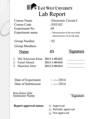
Lab ReportCourse NameCourse CodeExperiment NoExperiment name: Electronic Circuit-I: EEE102:05: Measurement of the non idealGroup NumberGroup Members: 02:Namecharacteristics of an Op-ampID1. Md. Solayman Khan 2013-1-80-0222. Faisal Ahmed2013-1-80-0163. Shamima Akter2012-3-80-014Date of ExperimentDate of SubmissionRony Kumer SahaInstructor NameReport approval status:Signature: --/--/2014: --/--/2014SignatureApprovedPartially approvedNot approved
AbstractAn operational amplifier (op-amp) is a DC-coupled high-gain electronic voltage amplifier with adifferential input and, usually, a single-ended output. In this configuration, an op-amp producesan output potential (relative to circuit ground) that is typically hundreds of thousands of timeslarger than the potential difference between its input terminals .Operational amplifiers had theirorigins in analog computers where they were used to do mathematical operations in many linear,non-linear and frequency-dependent circuits. Characteristics of a circuit using an op-amp are setby external components with little dependence on temperature changes or manufacturingvariations in the op-amp itself, which makes op-amps popular building blocks for circuit design.Op-amps are among the most widely used electronic devices today, being used in a vast array ofconsumer, industrial, and scientific devices. Many standard IC op-amps cost only a few cents inmoderate production volume. Op-amps may be packaged as components, or used as elements ofmore complex integrated circuits.
5.1 Objective Of The ExperimentThe main object of this experiment is to familiar with non ideal characteristics of an op- amp. Todo so, following works should be performed.1. To design electrical circuit with 741 op-amp and other relevant sources.2. To set up the circuit with multimeter by proper connections and sources to calculate thevoltages.3. To find the perfect values and error and comes to an conclusion on how to overcome.5.2 Significance of the ExperimentThe 741 Operational Amplifier is probably the most versatile Integrated Circuit available. It isvery cheap especially keeping in mind the fact that it contains several hundred components. TheOP AMP is a ‘Linear Amplifier’ with an amazing variety of uses. Its main purpose is to amplify(increase) a weak signal - a little like a Darlington Pair.5.3 TheoryThe op-amp manufacturer usually specifies the average value of I B1 andI B2 as well as their expected difference. The average value I B is called the input bias currentIB ( I B1 I B2 ) /2And the difference is called the input offset current and is given byIOS I B1 –IB2 5.4 Experimental Setup1. Op-Amp (uA741)2. Resistor (10KΩ 3pcs, 1KΩ 1pc, 4.7KΩ 1pc )3. DC multimeter
Circuit DiagramFig1(a): Circuit for measurement the offset voltage & bias current.Fig1(b): Circuit for measurement the offset voltage & bias current.
5.5 Experimental Procedure (Off-set voltage and Current )1. Measure the value of resistance. Contrast the circuit with resistance values R 1 R 2 10KΩ.we use 15 or – 15 volts from the trainer board for biasing the Op-Amp.2. Measure the output voltage V O1 with R 1 open and V O2 with R 1 grounded. From those tworeadings we calculate the off-set voltage form V OS (V O2 - V O1 ) R 1 / R 2 and the input biascurrent from I B1 (V O2 - V O1 ) /R 23. Let R 3 10KΩ to construct the circuit of fig1(b) and measure output voltage. With the outputvoltage from Fig. 1(b) and the input bias current IB1 from Fig. 1(a), use the relation derived inyour pre-lab to calculate the input bias current IB2.4. Now replace R3 by 4.7KΩ and measure V0 and IB2.5. Calculate the input offset and input bias currents from I OS I B1 –IB2 and IB (I B1 –IB2 )/25.5 Experimental Procedure ( Slew rate and Frequency response )1. Construct the circuit shown in Fig. 2. U se R1 1KΩ and R2 10KΩ and 15V from thetrainer board for biasing the op-amp.2. Use a 1V peak, 100Hz sine wave Vin from the signal generator and observe the output inchannel-2 and input in channel-1 using the dual mode of oscilloscope.3. Now change the input frequency from 100Hz to the maximum value where the output showsthe undistorted wave form. Write down this frequency and the amplitude of the input signal atthis frequency. Calculate the SR using the equation derived in prelab.4. Set the input frequency to 100Hz and measure the amplitudes of input and output signals andcalculate the gain.5. Now raise the frequency of the signal generator (do not change the input amplitude) to thevalue at which the output amplitude reduces to 0.707 of its 100Hz value. Write this frequency asf3. Measure the output amplitudes at the following frequencies, f3/4, f3/2, 2f3, 5f3, and10f3.Calculate the gain at f3/4, f3/2, f3, 2f3, 5f3, and 10f3.
5.6 Measurement and DataR 1 10.04KΩ,R 2 9.94KΩR 3 9.9KΩFor fig 1V O1 -0.9mVV OS V O1 /(1 R 2 /R 1 ) 0.9 10 3 /(1 9.94/10.04) -40.52mVFor fig 2I B1 V O1 / R 2 -0.9 10 3 / 9.94 103 97.4nAFor fig 3V O2 -0.5mVIB2 V O2 /R 3 50.5nAI OS I B1 –IB2 97.4 – 50.5 47.5nAI B (I B1 –IB2 )/2 (47.5)/2 23.75nAFor fig 4SR AV O /dt max 1V/2.52ms 396.8V/sA V - (R 2 /R 1 ) - (-9.94/10.04) -0.99ω 3db 257 KHzω t 257 1.99 511.4 KHz
5.7 Necessary CalculationFor fig 1V O1 -0.9mVV OS V O1 /(1 R 2 /R 1 ) 0.9 10 3 /(1 9.94/10.04) -40.52mVFor fig 2I B1 V O1 / R 2 -0.9 10 3 / 9.94 103 97.4nAFor fig 3V O2 -0.5mVIB2 V O2 /R 3 50.5nAI OS I B1 –IB2 97.4 – 50.5 47.5nAI B (I B1 –IB2 )/2 (47.5)/2 23.75nAFor fig 4SR AV O /dt max 1V/2.52ms 396.8V/sA V - (R 2 /R 1 ) - (-9.94/10.04) -0.99ω 3db 257 KHzω t 257 1.99 511.4 KHz
5.8 ResultsV OS -40.52mVI B1 97.4nAI B2 50.5nAI OS 47.5nAI B 23.75nASR 396.8V/sA V -0.99ω 3db 257 KHzω t 511.4 KHz5.9 Key findingsI. The output attempts to do whatever is necessary to make the voltage difference between theinputs zero.II. The inputs draw no current.III. 741 operational amplifiers suffer from several non-ideal effects.
5.10 Answer to the Report QuestionAnswer to the Report Question 01V 01 Vos IB1 R 2 (1)And,𝑅𝑅2V 02 V OS ( 1 𝑅𝑅1 ) I B1 R 2 (2)𝑅𝑅2(2)-(1) V O2 – V 01 V OS ( 1 𝑅𝑅1 ) - Vos And,𝑅𝑅2V O2 – V 01 V OS (𝑅𝑅1 )𝑅𝑅1V OS ( V O2 – V 01 )(𝑅𝑅2 )I B1 (V O2 – V 01 )/ R 1
Answer to the Report Question 021098Gain (A)765432-1101010Frequency (f)10321010Figure: Figure of gain-freq curveAnswer to the Report Question 0310X: 13.72Y : 9.61898Gain (A)7654X: 273Y : 2.6732-1101010Frequency (f)10321010Figure: Figure to determine the slope of the curveSlope (9.218-2.27)/(23.3-9.72) 0.49dB/decadAnswer to the Report Question 041098Gain (A)7654X: 273Y : 2.6732-110010110Frequency (f)Figure: Figure to find unity gainUnity gain frequency 257db210310
Answer to the Report Question 05Figure : Figure for the circuit to find offset voltage, offdet current and Bias currentVos V OS ( -755.41uv – 831.23uv )(1 ) -1.58mvIos 0.4nAI B 79.75nAComparison between simulation and 4nA.475nAIB79.75nA73.95nA
Answer to the Report Question 06Figure : Figure for the circuit to find SRFigure : Curve of output using square wave inputSR dVodt 4.5815 V 10.562us 0.433V/us
5.11 Conclusion and DiscussionThe LM741 series are general purpose operational amplifiers which feature improvedperformance over industry standards like the LM709.One of the practical op-amp limitations is that the inputs must stay within a certain voltage range(usually significantly less than the supply voltages) for proper operation. Op-amps are subject todrastic gain changes and bizarre behavior if these ranges are exceeded. For a 741 operating on /-15 volts, the common mode input swing should be within /-15 volts. Voltages over 15V maydamage the op-amp, regardless of the supply voltage. Some op-amps are designed to allowcommon mode voltages down to the negative supply voltage (LM358, 3130/3140) or up to thepositive supply (301/307 or 355-357).5.12 References Design with Operational Amplifiers and Analog Integrated Circuits; 4th Ed; Sergio Franco;McGraw Hill; 672 pages; 2014; ISBN 978-0078028168.Op Amps For Everyone; 4th Ed; Ron Mancini; Newnes; 304 pages; 2013; ISBN 9780123914958.Small Signal Audio Design; Douglas Self; Focal Press; 556 pages; 2010; ISBN 978-0-24052177-0.Op Amp Applications Handbook; Walt G. Jung; Newnes; 896 pages; 2004; ISBN 9780750678445.Op Amps and Linear Integrated Circuits; James M. Fiore; Cengage Learning; 616 pages;2000; ISBN 978-0766817937.Operational Amplifiers and Linear Integrated Circuits; 6th Ed; Robert F Coughlin; PrenticeHall; 529 pages; 2000; ISBN 978-0130149916.Op-Amps and Linear Integrated Circuits; 4th Ed; Ram Gayakwad; Prentice Hall; 543 pages;Engineer's Mini-Notebook – OpAmp IC Circuits; Forrest Mims III; Radio Shack; 49 pages;1985; ASIN B000DZG196.
5.13 AttachmentSinged data sheet.5.14 AppendicesOne application for the circuit would be to keep a "running total" of radiation exposure, or dosage, if theinput voltage was a proportional signal supplied by an electronic radiation detector. Nuclear radiationcan be just as damaging at low intensities for long periods of time as it is at high intensities for shortperiods of time.5.15 Further Reading1. Jacob Millman, Microelectronics: Digital and Analog Circuits and Systems, McGraw-Hill,1979, ISBN 0-07-042327-X, pp. 523-5272.D.F. Stout Handbook of Operational Amplifier Circuit Design (McGraw-Hill, 1976, ISBN 007-061797-X ) pp. 1–11.3. King, Grayson; Watkins, Tim (13 May 1999). "Bootstrapping your op amp yields widevoltage swings". Electronic Design News. Retrieved 2012-12-27.
Op Amps and Linear Integrated Circuits; James M. Fiore; Cengage Learning; 616 pages; 2000; ISBN 978-0766817937. Operational Amplifiers and Linear Integrat